

Page 1
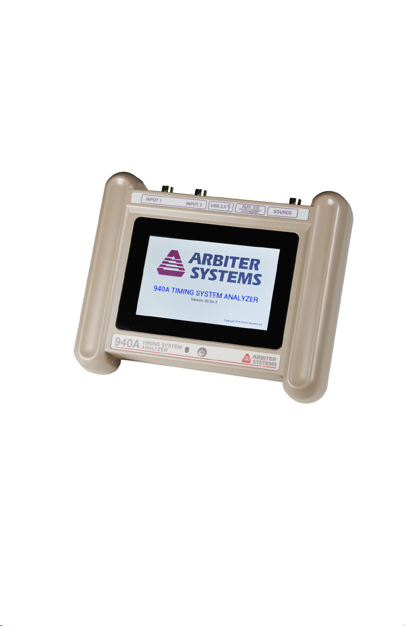
MODEL 940A
TIMING SYSTEM ANALYZER
USER’S MANUAL
Arbiter Systems, Inc.
Paso Robles, CA 93446
U.S.A.
FONK
informes@fonkel.com.mx
L MEXICANA
E
Tel: (55) 55 33 61 14
www.fonkel.com.mx
Page 2

Notice
This manual is issued for reference only, at the convenience of Arbiter Systems. Reasonable effort was made to verify that all contents were accurate as of the time of publication. Check with Arbiter Systems at the address below for any revisions made since the
original date of publication, found on page v.
ii
Page 3

LIMITED WARRANTY
Arbiter Systems makes no warranty, expressed or implied, on any
product manufactured or sold by Arbiter Systems except for the
following limited warranty against defects in materials and workmanship on products manufactured by Arbiter Systems.
Products manufactured by Arbiter Systems are guaranteed against
defective materials and workmanship under normal use and service
for one year from the date of delivery. The responsibility of Arbiter
Systems under this warranty is limited to repair or replacement,
at Arbiter Systems’ option, of any product found to be defective.
Arbiter Systems shall have no liability under this warranty unless
it receives written notice of any claimed defect, within the earlier
of:
• Thirty days of discovery by Buyer, or;
• One year from the date of delivery.
For warranty service or repair, products must be returned to a
service facility designated by Arbiter Systems. Buyer shall prepay
all shipping charges to Arbiter Systems, and Arbiter Systems shall
pay shipping charges, via ground, incurred in returning the product
to Buyer. However, Buyer shall pay all shipping charges, duties and
taxes for products returned to Buyer in a country other than the
United States of America.
THE WARRANTY SET FORTH HEREIN CONSTITUTES
THE ONLY WARRANTY OBLIGATIONS OF ARBITER
SYSTEMS, EXPRESSED OR IMPLIED, STATUTORY, BY
OPERATION OF LAW, OR OTHERWISE. ARBITER
SYSTEMS DISCLAIMS ANY WARRANTY OF
MERCHANTABILITY OR FITNESS FOR A PARTICULAR
PURPOSE, AND BUYER EXPRESSLY WAIVES ALL OTHER
WARRANTIES.
This limited warranty does not extend to any product, which has
been subject to:
I Improper use or application, abuse, or operation beyond its
rated capacity, or contrary to the instructions in the operation
and maintenance manuals (if any);
II Accident;
III Repair or maintenance performed by Buyer, except in accor-
dance with the operation and maintenance manuals, if any,
and any special instructions of Arbiter Systems;
IV Modification without the prior written authorization of Ar-
biter Systems (whether by the substitution of non-approved
iii
Page 4

parts or otherwise).
The remedies provided herein are Buyer’s sole and exclusive remedies. In no event shall Arbiter Systems be liable for direct, indirect, incidental or consequential damages (including loss of profits),
whether based on contract, tort, or other legal theory.
FOR THE FASTEST POSSIBLE SERVICE,
PLEASE PROCEED AS FOLLOWS:
1. Notify Arbiter Systems, Inc., specifying the instrument model
number and serial number and giving full details of the difficulty. Service data or instrument-return authorization will
be provided upon receipt of this information.
2. If instrument return is authorized, forward prepaid to the
manufacturer. If it is determined that the instrument is not
covered by this warranty, an estimate will be made before the
repair work begins, if requested.
See Contact Information on page ii.
iv
Page 5

Arbiter Systems, Inc.
Model 940A
Timing System Analyzer™
User’s Manual
Notice & Contact
Warranty
Contents
Features
Connecting Timing Signals
Setup Screens
Viewing Timecodes
Specifications
940A Utility Software
Appendix A – IRIG-B Information
Copyright ©Arbiter Systems Incorporated June 2017 All rights
reserved. International copyright secured.
PD0054700 Revision A
A pdf version of this manual is available for download at
www.arbiter.com. To reorder the printed manual contact Arbiter
Sales and order Part No. AS0106800.
v
Page 6

Contents
Features 1
Special Features . . . . . . . . . . . . . . . . . . . . . . . 1
Construction . . . . . . . . . . . . . . . . . . . . . . . . . 2
Input/Output Connectors . . . . . . . . . . . . . . . 2
AUX Port . . . . . . . . . . . . . . . . . . . . . . . . 2
Micro USB Port . . . . . . . . . . . . . . . . . . . . 2
Flashlight . . . . . . . . . . . . . . . . . . . . . . . . 2
Power Supply and Charging . . . . . . . . . . . . . . . . . 3
Battery charging . . . . . . . . . . . . . . . . . . . . 3
Operating with Power Supply/Charger . . . . . . . . 3
Powering ON or OFF . . . . . . . . . . . . . . . . . 3
Battery Indication . . . . . . . . . . . . . . . . . . . 3
Model 940A Accessories . . . . . . . . . . . . . . . . . . . 4
Connecting Time Signals 5
Coaxial Cable . . . . . . . . . . . . . . . . . . . . . . . . . 5
Twisted Pair Cable . . . . . . . . . . . . . . . . . . . . . . 6
Setup Screens 7
Buttons & Screens . . . . . . . . . . . . . . . . . . . . . . 7
The Home Screen . . . . . . . . . . . . . . . . . . . . 7
Navigating the Menus . . . . . . . . . . . . . . . . . 8
The Home Button . . . . . . . . . . . . . . . . . . . 8
Gear Button . . . . . . . . . . . . . . . . . . . . . . 8
Return Button . . . . . . . . . . . . . . . . . . . . . 8
Pause Button . . . . . . . . . . . . . . . . . . . . . . 8
Play Button . . . . . . . . . . . . . . . . . . . . . . . 8
Slider Bar . . . . . . . . . . . . . . . . . . . . . . . . 8
Configuring Input 1 . . . . . . . . . . . . . . . . . . 9
Configuring Input 2 . . . . . . . . . . . . . . . . . . 9
vi
Page 7

Viewing a Signal at Input 1 . . . . . . . . . . . . . . 10
Configuring the SOURCE . . . . . . . . . . . . . . . 11
IRIG Source Configuration . . . . . . . . . . . . . . 12
Custom Start Date and Time . . . . . . . . . . . . . 13
Source IRIG-B Bits . . . . . . . . . . . . . . . . . . . 14
Setting the DST Clock . . . . . . . . . . . . . . . . . 15
Unmodulated IRIG-B Source Level . . . . . . . . . . 16
Source DC Voltage Adjustment . . . . . . . . . . . . 17
Modulated IRIG-B Source Level . . . . . . . . . . . 18
Source Modulation Ratio . . . . . . . . . . . . . . . 19
Source 1 PPS Configuration . . . . . . . . . . . . . . 20
1 PPS Source Output Level . . . . . . . . . . . . . . 21
DCF77 Source Configuration . . . . . . . . . . . . . 22
System Configuration . . . . . . . . . . . . . . . . . . . . 23
System Menu Notes . . . . . . . . . . . . . . . . . . 24
Manually Setting the RTC . . . . . . . . . . . . . . . 25
Viewing Timecodes 26
DISPLAY Functions . . . . . . . . . . . . . . . . . . . . . 26
Waveform Comparisons . . . . . . . . . . . . . . . . 27
Unmodulated IRIG-B . . . . . . . . . . . . . . . . . . . . 28
Modulated IRIG-B . . . . . . . . . . . . . . . . . . . . . . 30
Input 1 PPS Timing . . . . . . . . . . . . . . . . . . . . . 31
Source 1 PPS Timing . . . . . . . . . . . . . . . . . . . . 32
DCF77 Timing . . . . . . . . . . . . . . . . . . . . . . . . 33
Specifications 35
The 940A Utility 37
Updating Firmware . . . . . . . . . . . . . . . . . . . . . . 37
Firmware Package . . . . . . . . . . . . . . . . . . . 37
Driver Software . . . . . . . . . . . . . . . . . . . . . 37
Updating the 940A . . . . . . . . . . . . . . . . . . . 37
IRIG-B Information 40
vii
Page 8

List of Figures
1 940A Connections . . . . . . . . . . . . . . . . . . . 5
2 Male BNC Breakout with Terminals . . . . . . . . . 6
3 The Home Screen at Startup . . . . . . . . . . . . . 7
4 Input 1 Configuration Screen . . . . . . . . . . . . . 9
5 Displayed Unmodulated IRIG-B Input . . . . . . . . 10
6 The Source Configuration Screen . . . . . . . . . . . 11
7 Configuring the IRIG-B Output . . . . . . . . . . . . 12
8 Set Custom Time Screen . . . . . . . . . . . . . . . . 13
9 Configuring the Source IRIG-B Bits . . . . . . . . . 14
10 Setting the DST Clock . . . . . . . . . . . . . . . . . 15
11 Configuring the Source Output Level . . . . . . . . . 16
12 Adjust the Source Voltage . . . . . . . . . . . . . . . 17
13 Modulated IRIG Source Output Level . . . . . . . . 18
14 Adjust the Source AC Voltage . . . . . . . . . . . . . 18
15 Adjust the Source AC Modulation Ratio . . . . . . . 19
16 Configuring the 1 PPS Time Source . . . . . . . . . 20
17 Configuring the 1 PPS Output . . . . . . . . . . . . 21
18 Adjusting the 1 PPS Voltage . . . . . . . . . . . . . 21
19 Configuring the DCF77 Output . . . . . . . . . . . . 22
20 System Configuration . . . . . . . . . . . . . . . . . 23
21 Set Real Time Clock Screen . . . . . . . . . . . . . . 25
22 DISPLAY on the Home Screen . . . . . . . . . . . . 26
23 1 PPS & IRIG-B Waveforms . . . . . . . . . . . . . 27
24 Unmodulated IRIG-B Display . . . . . . . . . . . . . 28
25 Pulse Jitter . . . . . . . . . . . . . . . . . . . . . . . 29
26 Modulated IRIG-B . . . . . . . . . . . . . . . . . . . 30
27 1 PPS Signal Connected to Input 1 . . . . . . . . . . 31
28 1 PPS Signal at Source Connector . . . . . . . . . . 32
29 DCF77 Signal Connected to Input 2 . . . . . . . . . 33
viii
Page 9

30 DCF77 Signal Elements . . . . . . . . . . . . . . . . 34
31 940A Utility Opening . . . . . . . . . . . . . . . . . 37
32 Selecting COM Port . . . . . . . . . . . . . . . . . . 38
33 940A Utility Reading Serial Number . . . . . . . . . 38
34 940A Firmware Ready to Upload . . . . . . . . . . . 39
35 940A Upload Progress . . . . . . . . . . . . . . . . . 39
ix
Page 10

x
Page 11

Features
The Model 940A is a powerful diagnostic tool for analyzing timecodes in time sensitive instruments. IRIG-B, DCF77 and 1 PPS
signals can be received and evaluated to verify correct operation.
These signals may also be sourced from the 940A to verify operation of the receiving equipment.
Operating on four Li-ion batteries, the 940A can run continually
for about 12 hours with about 80 percent backlight brightness, and
for about 24 hours at 20 percent brightness. Included in a 940A kit
are the following: USB charger/power supply, USB Cable, 8 feet of
RG-58 with BNC connectors, quick setup guide, and several cable
adapters to match a variety of wire types and connectors.
The 940A features two timing input ports, one timing source
output port, a mini USB charging port, variable output flashlight,
speaker and auxiliary port.
Available input signals are unmodulated IRIG-B, modulated
IRIG-B, IRIG-B Manchester, 1 Pulse Per Second and DCF77.
Three different load conditions are available, which are Load Off,
100 Ohm Load and 50 Ohm Load.
Special Features
Model 940A is designed to provide both a pictorial view and a
description of signals connected to either Input 1 or Input 2. It
also provides a method to compare two signals connected to Input
1 and 2.
A timing source output is also available to verify devices re-
ceiving these signals. Available timing output signals include unmodulated IRIG-B, modulated IRIG-B, 1 Pulse Per Second and
DCF-77.
1
Page 12

Multi-View Display
In the display’s descriptive view, you can read all the values provided in the timecode, such as time, date, day or year, time offset, leap second information and the state of daylight saving time.
Other useful information includes jitter error, time difference (Input 1 - Input 2) and signal amplitude in volts.
Additionally, the 940A provides a time domain display much
like an oscilloscope. In this mode, each bit of the time code is
identified, and may be verified with the specification.
Construction
Constructed of tough polycarbonate/polyester alloy, the 940A case
was designed for durability and easy handling. It has a 5-inch
diagonal, color graphic, touch screen display made of tempered,
scratch-resistant glass, with self-adjusting brightness controls. A
bail assembly is useful for propping up the instrument. Input and
output connections are through female BNC connectors.
Input/Output Connectors
Two female BNC connectors are available for connecting two different input signals. One female BNC connector is available to source
any timing signal selection in the 940A.
AUX Port
The RJ-45 port is available for further development of features and
accessories.
Micro USB Port
A micro USB port is available for charging the internal Li-Ion batteries, powering the 940A and updating firmware.
Flashlight
An LED flashlight is available near the micro USB port with variable brightness control.
2
Page 13
Power Supply and Charging
100%
52% H
15%
The Model 940A can operate from the included power supply/charger, or from the internal Li-ion batteries. Internal batteries
consist of four 2250 milliampere hour Li-ion cells, which should be
able to operate the 940A for up to 18 hours with reduced backlight.
Battery charging
A micro USB connector is used to connect the included battery
charger/power supply to 940A. Depending on the state of charge,
charging time should be less than 8 hours, or longer if the batteries
are completely depleted. Fully charged, the 940A should operate
for up to 24 hours with the display backlight set to 20 percent
brightness, and the flash light and the speaker switched off.
Operating with Power Supply/Charger
With the included power adapter/charger connected, the 940A
should operate indefinitely.
Powering ON or OFF
Press (the ON/OFF button) at the bottom of the front panel
to energize and de-energize the 940A.
Battery Indication
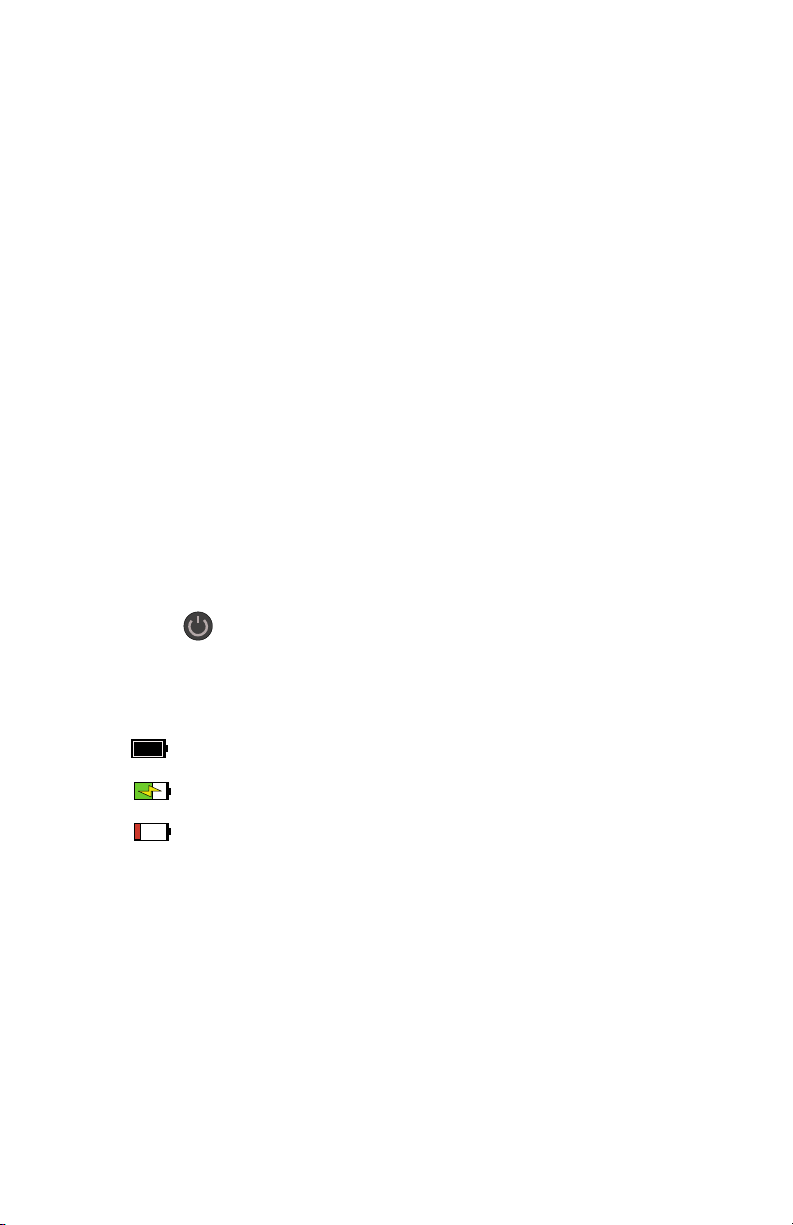
Charged, not connected to charger
Charging High, connected to charger
Battery very low, connect to charger!
Charging Characteristics
While charging, text below the battery symbol indicates the percentage of charge remaining and a small letter to indicates the
charge rate, which depends on the type of charger and USB cable.
Three letters indicate the charging rate: L for low (100 mA),
M for medium (500 mA) and H for high (1000 mA – with included
charger/cable). Both the AC Adapter/Charger and the cable contribute to the charging rate.
3
Page 14
Checking Battery Status
Check the battery status while the unit is turned off and being
charged by pressing the ON/OFF button quickly.
Model 940A Accessories
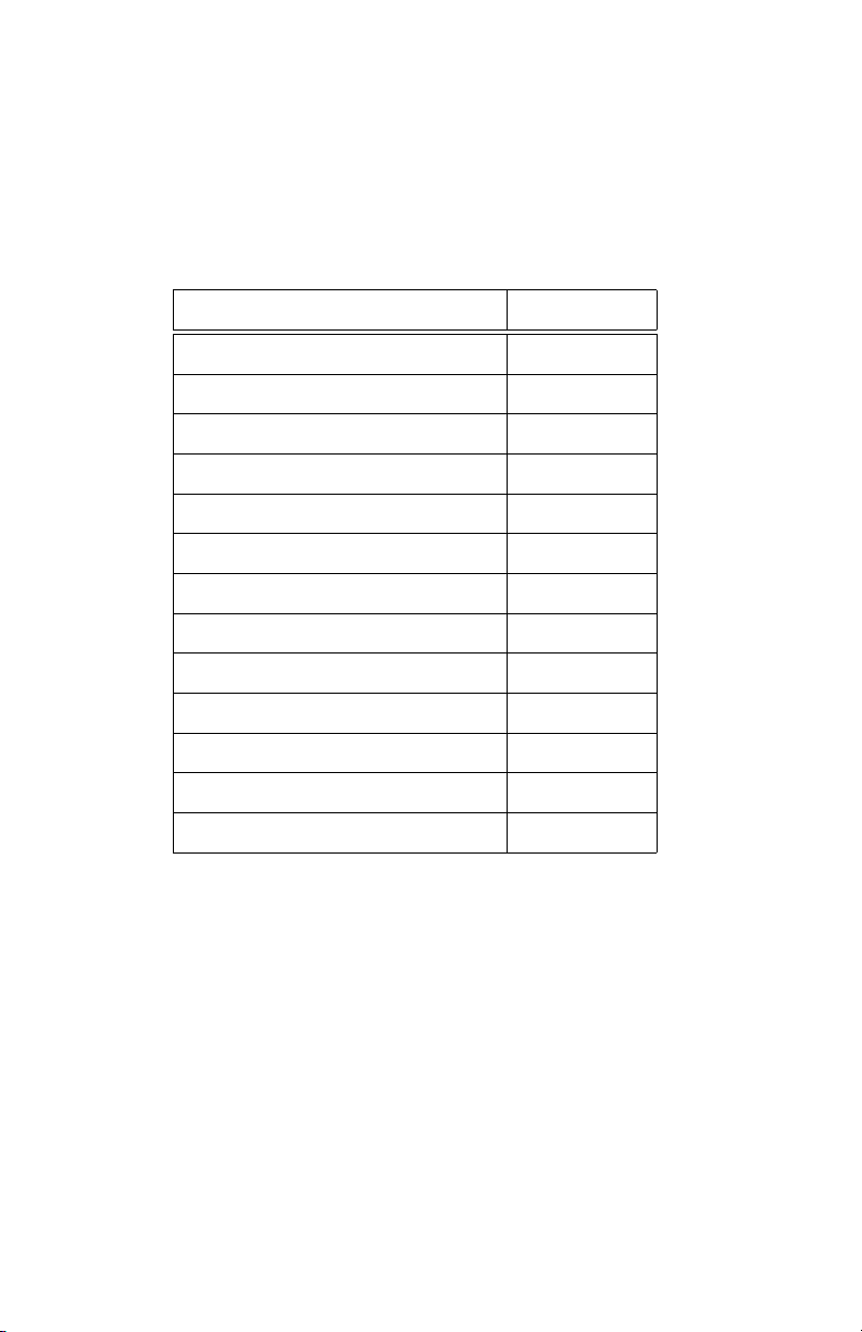
Part Description Part No.
BNC Breakout M to Wires AP0003400
BNC Barrel (F-F) CN0003400
BNC Breakout F to Wires AP0008900*
BNC Adapt M to 2 Pos Term. AP0014900*
BNC M to 2 Screw Term AP0015000
USB 2.1A Wall Charger AP0015300*
Quick Setup Guide PD0055400*
940A Printed Operation Manual AS0106800
USB 2.0A Male to Micro Cable CA0033700*
BNC Coax Cable M/M CA0033808*
BNC ”T”Conn F-M-F CN0003500*
Terminal Block, Plug 2 Pin CN0019202*
Case Soft 940A HD0068600*
Table 1: 940A Accessories, *Included
4
Page 15
Connecting Time
Source (output)
USB - charging,
firmware update
Input 2Input 1
FlashlightSpeaker
(under bail assembly)
Bail
Auxiliary I/O Port
Signals
This section describes how and where to connect the input and
output signals in the Model 940A.
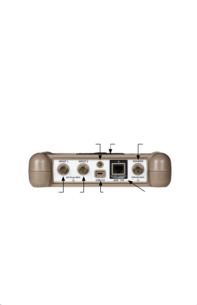
The Model 940A has three standard BNC connectors for connecting the two inputs and one output, as seen in Figure 1. Coaxial
cable and shielded, twisted-pair cable are the most commonly used
cable types used with timing equipment.
Figure 1: 940A Connections and Features
The source, BNC connector is seen on the right; the two input
BNC connectors are on the left. A micro USB is between the Input
2 and AUX I/O port and a flashlight is located above the micro
USB port.
Coaxial Cable
Input and output timing connectors on the Model 940A are female
BNC, which is one of the most common connectors being used on
electrical equipment today. Coaxial cables are usually fitted with
5
Page 16
male BNC connectors, which connect directly to the 940A.
Twisted Pair Cable
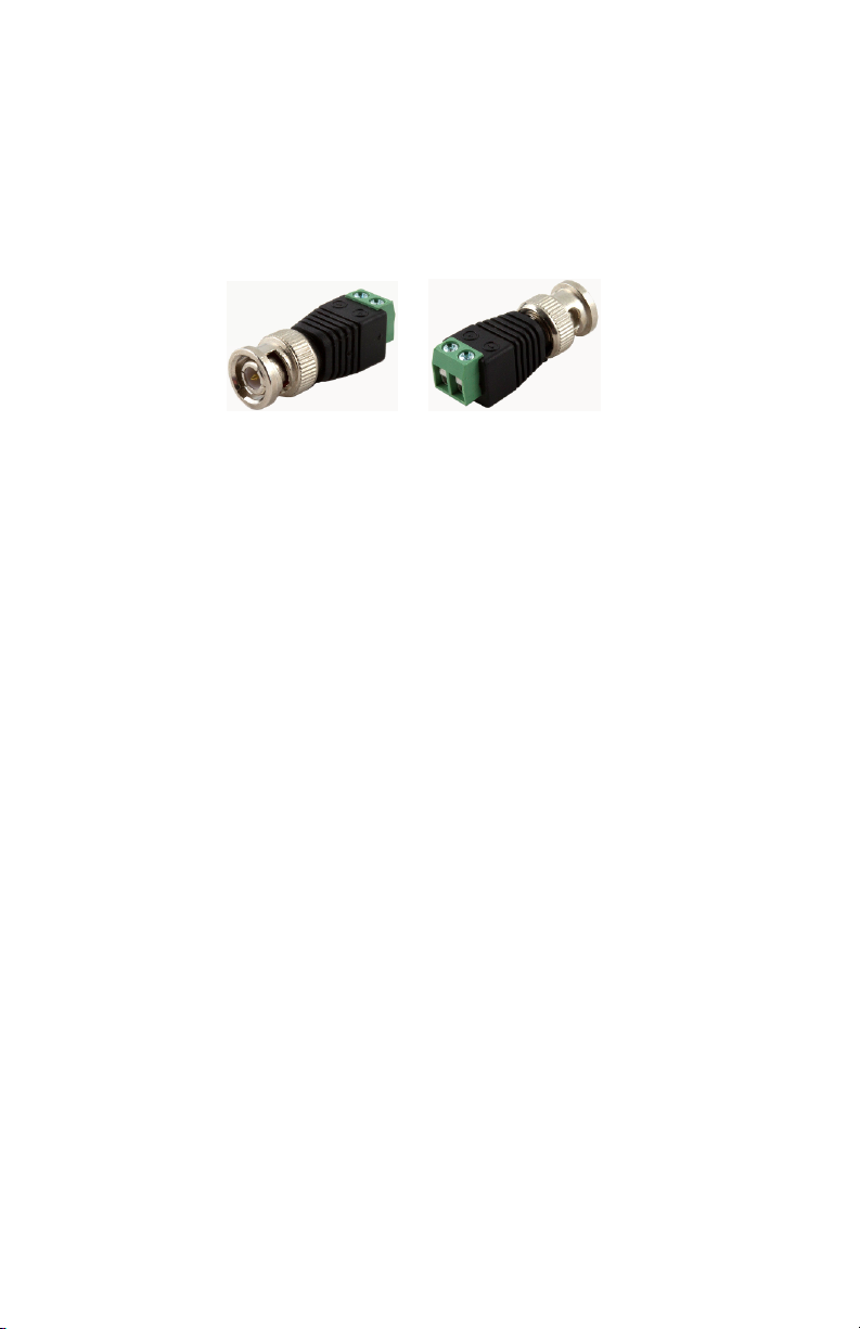
To adapt a twisted pair of wires to the female BNC input connector
on the Model 940A, use a BNC breakout as pictured in Figure 2.
Figure 2: Male BNC Breakout with Terminals
Connecting
Connect the breakout’s male BNC connector to the 940A, then attach the twisted pair of wires to the breakout terminals and tighten
the screws. Make sure to observe the polarity marking on the
breakout. Do not tin stranded wire with solder.
6
Page 17
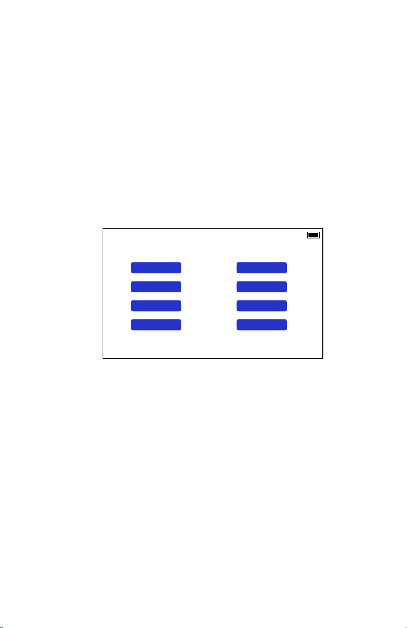
Setup Screens
CONFIGURATION DISPLAY
INPUT 1 INPUT 1
INPUT 2 INPUT 2
SOURCE
SOURCE
SYSTEM
INPUT 1+2
100%
Buttons & Screens
The Home Screen
Figure 3: The Home Screen at Startup
Figure 3 illustrates the Home screen. From the Home screen you
can configure Input 1 and 2, the Source (signal output) and System
parameters, which include flashlight brightness, speaker volume,
display back light, and Real Time Clock (RTC). You only need to
touch the screen buttons to make choices. When first powering on
the 940A, it should display a startup message, as seen on page i,
and then display the home screen, as seen above.
7
Page 18

Navigating the Menus
With reference to Figure 3, there are two HOME menus – CONFIGURATION and DISPLAY – with different buttons within each
menu.
TOUCH ACTIVATED AREAS ARE BLUE
The Home Button
appears in the bottom left corner of most screens, except of
course, the home screen. This symbol is used to return to the
home screen from other menus.
Gear Button
shows up when further configuration is possible, or needed. It
only appears when selecting a specific signal, but not if selecting
DISABLED.
Return Button
is normally found in the lower right corner of the display. Touch
the return button to go back to the previous menu.
Pause Button
is used to freeze the display when viewing a timing signal to
capture the various bits for longer viewing.
Play Button
is used to resume showing the active display after pressing the
pause button.
Slider Bar
is used to move along the displayed time code to
view other elements not in the current display.
8
Page 19
Configuring Input 1
Load Off
100 Ohm Load
50 Ohm Load
Compensate for
1 Second Delay
INPUT 1 CONFIGURATION
IRIG-B UNMODULATED
IRIG-B MODULATED
IRIG-B MANCHESTER
1 PULSE PER SECOND
DCF77
DISABLED
100%
INPUT 1
INPUT 2
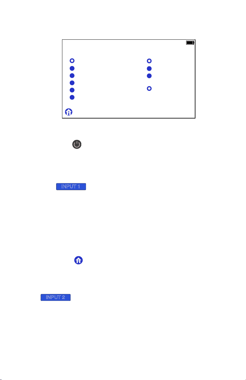
Figure 4: Input 1 Configuration Screen
1. Press to power on the 940A.
2. Connect the cable from the equipment you want to test to
Input 1.
3. In the Home screen CONFIGURATION menu, touch
.
4. In INPUT 1 CONFIGURATION display (see Figure 4) touch
the desired signal. For example, IRIG-B UNMODULATED.
Configuring Input 2
From the Home screen CONFIGURATION menu, touch
put 1 as described above.
5. Touch one of the Load configuration buttons, such as Load
Off.
6. Touch the Compensate for 1 Second Delay, if required. Keeps
the 940A time in sync with source.
7. Touch when finished.
. Otherwise, the setup should be the same as for In-
9
Page 20
Viewing a Signal at Input 1
INPUT 1
INPUT 1 IRIG-B UNMODULATED
Time: 00:55:46 UTC
Date: 01 JUL 2015
DOY: 182
SBS:3346
Time Offset: 0
TQ: Locked
CTQ: <100ns
LSP: 0 LSD: 0
DSP: 0 DST: 0
PARITY: EVEN
Jitter: 0.47 uS, 0.1 RMS
In1 - In2 Delta T: ---.- uSecs
Amplitude: 4.1 Volts
Year(15) Offset(0) TQ(6)
20 40 80
P6 LSP DSP DST SIGN 1 2 4 8LSD
56 57 58 59 60 61 62 63 64 65 66 67 68 69 70
100% H
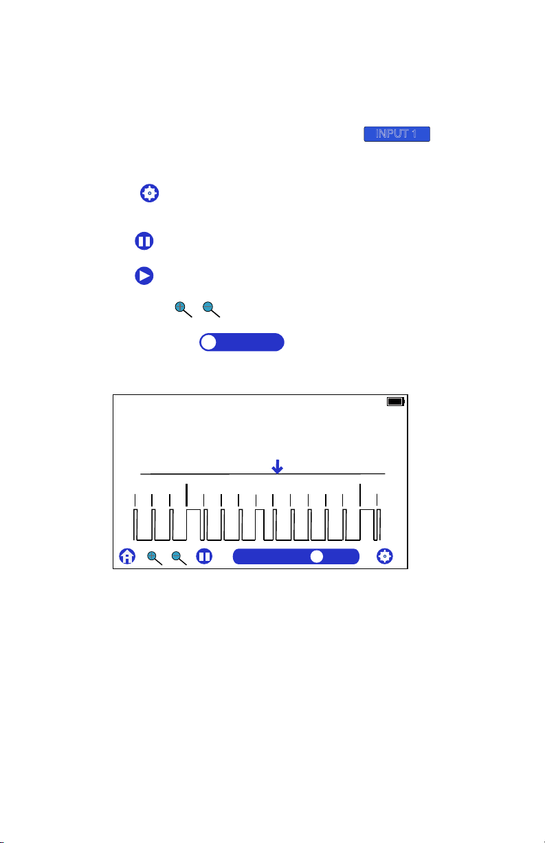
Continue from the previous page by connecting an unmodulated
IRIG-B signal to Input 1.
1. In the Home screen DISPLAY menu, touch
.
2. The input 1 display could look similar to Figure 5.
3. Touch if necessary to change the 940A mode to IRIG-B
UNMODULATED.
4. Press to pause (freeze) the active signal in the display.
5. Press to resume displaying the active signal.
6. Press either to zoom in or out in the display.
7. Touch and slide to view other sections of the
IRIG-B signal.
Figure 5: Displayed Unmodulated IRIG-B Input
For more information on viewing input signals see page 26 re-
garding Viewing Timecodes.
10
Page 21
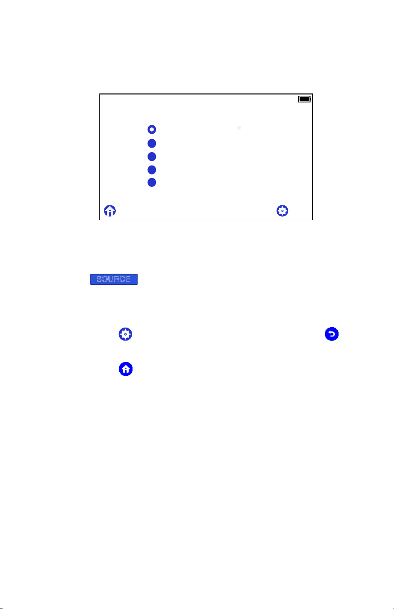
Configuring the SOURCE
SOURCE SIGNAL SELECTION
IRIG-B UNMODULATED
IRIG-B MODULATED
1 PULSE PER SECOND
DCF77
DISABLED
100%
SOURCE
Configuring the source is very similar to configuring either Input 1
or Input 2.
Figure 6: The Source Configuration Screen
1. In the Home screen CONFIGURATION menu, touch
.
2. In SOURCE SIGNAL SELECTION menu, touch desired sig-
nal – for example, IRIG-B UNMODULATED.
3. Touch to configure other time settings, then touch to
return to the SOURCE SIGNAL SELECTION menu.
4. Touch to return to the Home screen.
Once selected, the 940A produces the timing signal at source
connector. When DISABLED, the 940A will not display the gear
symbol.
11
Page 22
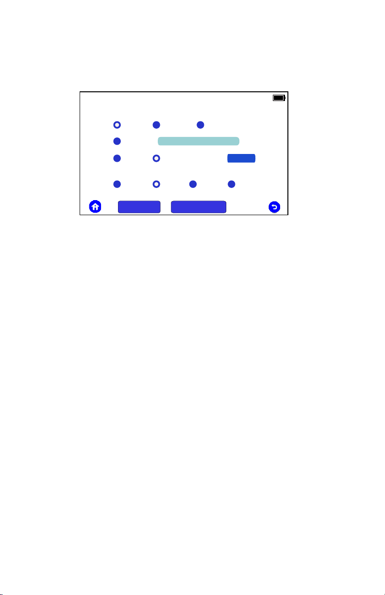
IRIG Source Configuration
SOURCE IRIG CONFIGURATION
Input1
UTC
2005 2011 OFF
YEAR ONLY
Local
Input2
Duplicate Input
Custom
TIME SOURCE
C37.118
APR 28, 2024 16:44:10
LOCAL OFFSET:
-8:00
IRIG-B BITS OUTPUT LEVEL
100% H
The source signal can come from Input 1, Input 2, or Custom.
Custom can generate its own signal.
Figure 7: Configuring the IRIG-B Output
Use for either modulated or unmodulated IRIG-B.
1. Touch the Input 1, Input 2, or Custom buttons to select
the signal source to transmit IRIG-B from the Source BNC
connector.
2. Touch the Duplicate Input button if you want to exactly reproduce at the source the signal connected to Input 1 or 2.
3. If wanting to set to a custom time and date, touch Custom,
then the Time/Date bar next to it – see page 13 to set the
date and time.
4. Select the time zone as UTC or Local. If Local, touch the
Local Offset value to adjust.
5. Touch one of the C37.118 values to set up the required standard, turn C37 values OFF, or switch year only ON.
12
Page 23
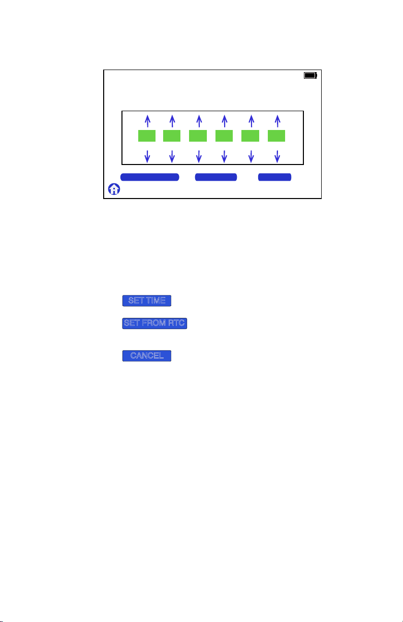
Custom Start Date and Time
SOURCE IRIG CONFIG
Custom User Time
SET FROM RTC SET TIME CANCEL
Month Day Ye ar Hour Minute Second
SEP 29 2016 12 34 56
100% H
SET TIME
SET FROM RTC
CANCEL
Figure 8: Set Custom Time Screen
Figure 8 illustrates the Custom Time window, which provides a
method to manually set the source date and time.
1. Touch the up or down arrows for each item of date and time.
2. Touch
3. Touch
Time Clock.
4. Touch
after setting the time and date.
to set the custom clock from the Real
to escape from this menu.
13
Page 24
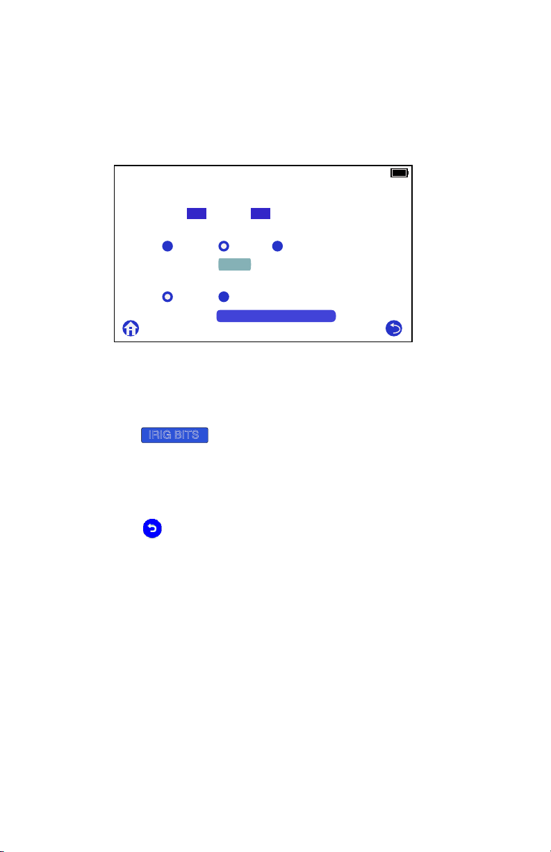
Source IRIG-B Bits
0
1
CONFIGURE SOURCE IRIG BITS
Enable
DEC
Enable DST Active
TQ: CTQ:
Add
Del
Time Quality Values
Leap Second Configuration
Daylight Saving Configuration
APR 28, 2024 16:44:10
Change Over Month:
Change Over Time:
100% H
IRIG BITS
IRIG-B Bits allows you to manipulate the IRIG bits to test time
quality and a time change, such as Leap Seconds and Daylight
Saving changes. One of the C37 values (i.e. 2005 or 2011 from
Figure 7) must be enabled for this menu to appear.
Figure 9: Configuring the Source IRIG-B Bits
1. Start from the configuration steps on page 12.
2. Touch
BITS menu as seen in Figure 9.
3. Make any changes to Time Quality, Leap Seconds and Daylight Saving Time selections.
4. Touch to return to the SOURCE IRIG CONFIGURATION menu.
NOTE: Changing any of these bits does NOT change the time in
the IRIG-B string. It only changes the specific Control Function
bits for diagnostic purposes.
To change the source time and date: use the Custom button
in the IRIG SOURCE CONFIGURATION menu.
to open the CONFIGURE SOURCE IRIG
14
Page 25
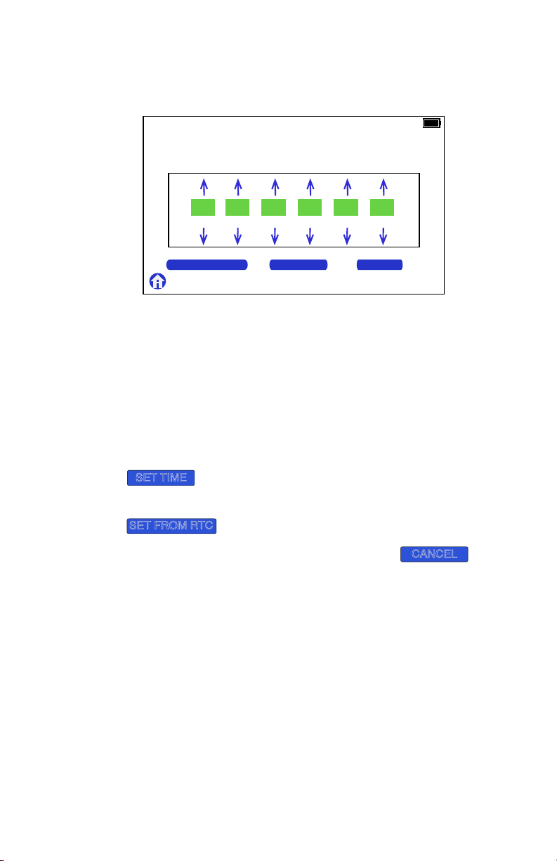
Setting the DST Clock
CONFIGURE SOURCE IRIG BITS
DST Change Over Time
SET FROM RTC SET TIME CANCEL
Month Day Ye ar Hour Minute Second
MAR 12 2017
2 00 00
100% H
SET TIME
SET FROM RTC
CANCEL
Manually sets the DST clock for a Daylight Saving Time event.
Figure 10: Setting the DST Clock
1. Touch the Change Over Time bar as seen at the bottom of
Figure 9.
2. From Figure 10, touch either the UP or DOWN arrows for
Month, Day, Year, Hour, Minute and Second.
3. When the preferred date and time is selected, touch
.
4. To set the changeover time from the Real Time Clock, touch
5. To return without applying anything, touch
.
.
15
Page 26
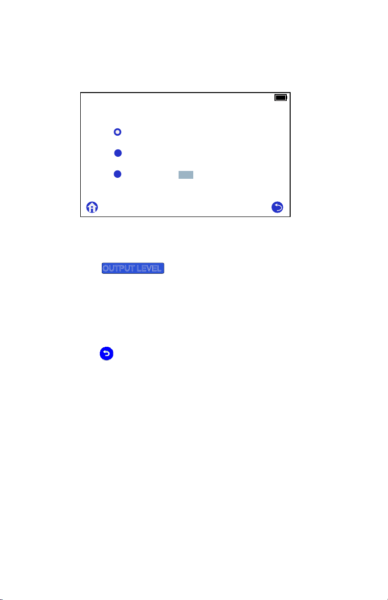
Unmodulated IRIG-B Source Level
SOURCE OUTPUT LEVEL
HI Drive with 50 Ohm
Variable
HI Drive (125ma @ 5V)
Vdc
5
100% H
OUTPUT LEVEL
Sets the drive level for the specific timing output source impedance
or voltage.
Figure 11: Configuring the Source Output Level
1. From the SOURCE IRIG CONFIGURATION menu screen,
touch
LEVEL menu screen.
2. Touch one of the three selection buttons.
3. If selecting Variable, touch the voltage button to open the
voltage adjustment screen – see Figure 12.
to open the SOURCE OUTPUT
4. Touch to go back to the SOURCE IRIG CONFIGURATION menu.
16
Page 27
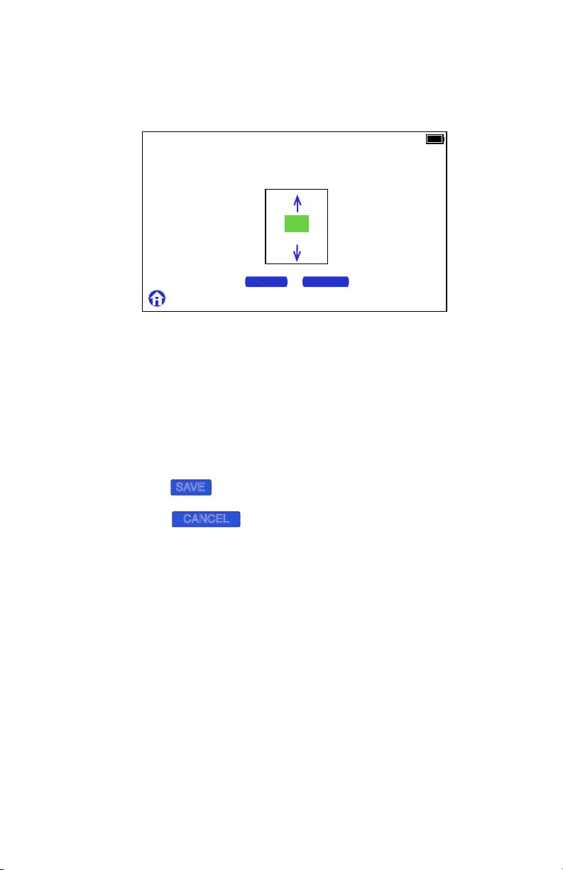
Source DC Voltage Adjustment
SOURCE OUTPUT LEVEL
Edit DC Amplitude
SAVE CANCEL
Volt s
5
100% H
SAVE
CANCEL
Use this menu to adjust the 940A source output voltage; works
with unmodulated IRIG-B and 1 PPS.
Figure 12: Adjust the Source Voltage
1. Touch the UP and DOWN arrows to adjust the IRIG-B unmodulated voltage level to your desired level.
Voltage range is from 1 to 15 Volts, with 50 ohm source
impedance.
2. Touch
to save the selected output voltage.
3. Touch
changing anything.
to return to the previous screen without
17
Page 28
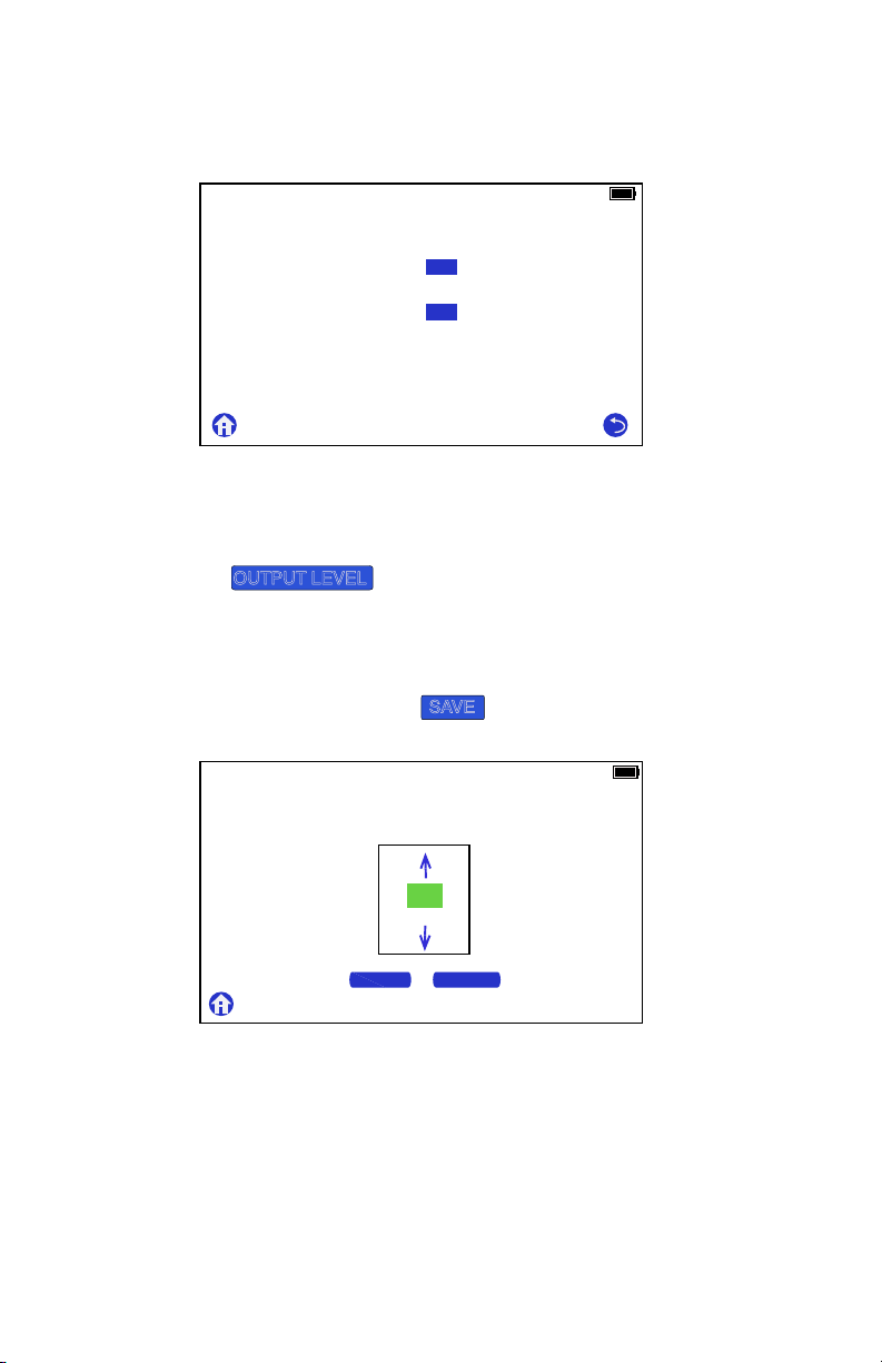
Modulated IRIG-B Source Level
SOURCE OUTPUT LEVEL
Modulation Ratio:
Variable
Vpeak
5
10:3
100% H
OUTPUT LEVEL
SAVE
SOURCE OUTPUT LEVEL
Edit AC Amplitude
SAVE CANCEL
Volt s
5
100% H
Sets the modulated IRIG-B peak voltage and the modulation ratio.
Figure 13: Modulated IRIG Source Output Level
1. From the SOURCE IRIG CONFIGURATION menu screen,
touch
LEVEL menu screen.
2. Touch Variable button to open the voltage adjustment
screen – see Figure 14. Voltage range is 1 to 10 V. Touch
the arrows to adjust, then
to open the SOURCE OUTPUT
.
Figure 14: Adjust the Source AC Voltage
18
Page 29
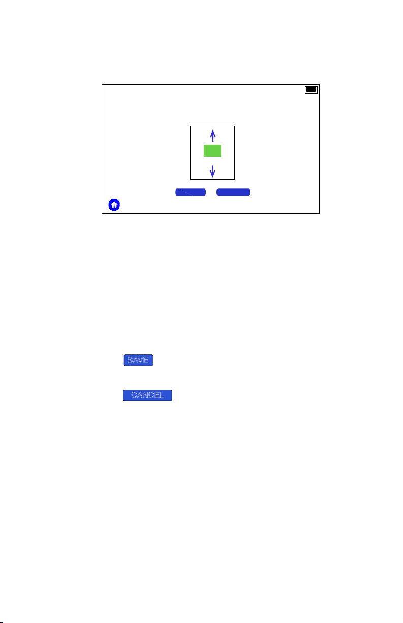
Source Modulation Ratio
SOURCE OUTPUT LEVEL
Edit Modulation Ratio
SAVE CANCEL
Ratio
10:3
100% H
SAVE
CANCEL
Sets the modulation ratio for modulated IRIG (B12x).
Figure 15: Adjust the Source AC Modulation Ratio
1. Touch the Modulation Ratio button to select the desired ratio
– includes 2:1, 3:1, 10:3, 4:1, 5:1, 6:1 and 7:1. Note: for
higher modulation ratios (e.g. 4:1 and higher), the Source
Output Level may need to be adjusted higher.
2. In the SOURCE OUTPUT LEVEL, Edit Modulation Ratio
screen, touch the UP or DOWN buttons to set the modulation ratio.
3. Touch
to store the new voltage and return to the
previous menu screen.
4. Touch
saving.
to return to the previous screen without
19
Page 30
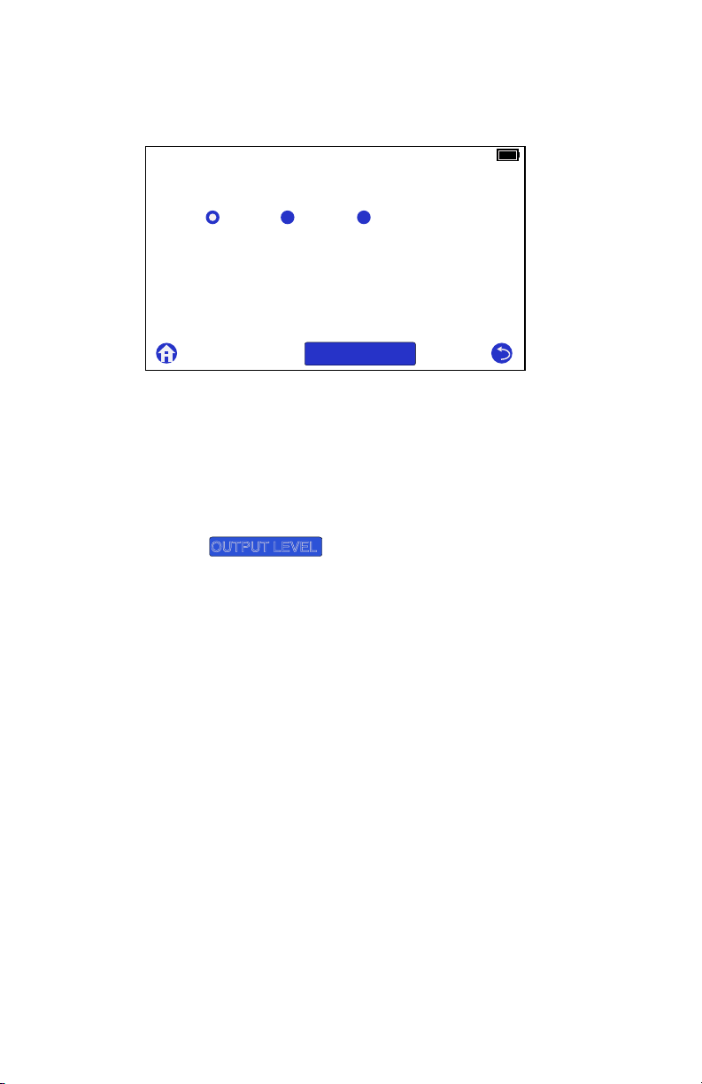
Source 1 PPS Configuration
SOURCE 1PPS CONFIGURATION
RTCInput1 Input2
100% H
TIME SOURCE
OUTPUT LEVEL
OUTPUT LEVEL
Sets the time signal source from either Input 1, Input 2 or RTC.
Figure 16: Configuring the 1 PPS Time Source
1. From the SOURCE SIGNAL SELECTION menu screen,
touch the 1 PULSE PER SECOND button.
2. Select the TIME SOURCE button: Input 1, Input 2 or RTC.
3. Touch the
ure 17.
to set the output voltage – see Fig-
20
Page 31
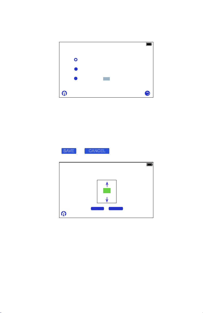
1 PPS Source Output Level
SOURCE OUTPUT LEVEL
HI Drive with 50 Ohm
Variable
HI Drive (125ma @ 5V)
Vdc
5
100% H
SAVEorCANCEL
SOURCE OUTPUT LEVEL
Edit AC Amplitude
SAVE CANCEL
Volt s
5
100% H
Sets the 1 PPS source output impendance and voltage.
Figure 17: Configuring the 1 PPS Output
1. Touch the Variable (50 Ohm Source) to open the SOURCE
OUTPUT LEVEL adjustment screen. See Figure 18.
2. Touch the UP or DOWN arrows to choose the desired voltage
level (1 Vpeak to 15 Vpeak).
3. Touch
Figure 18: Adjusting the 1 PPS Voltage
when finished.
21
Page 32
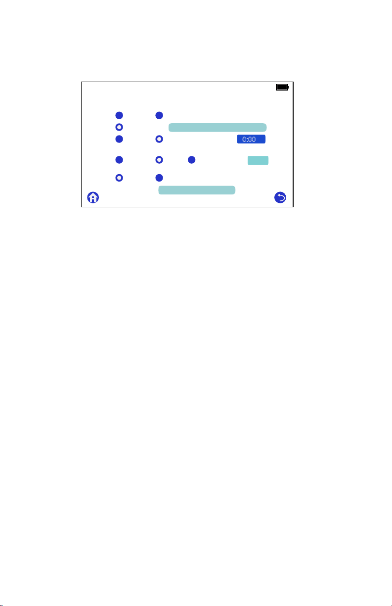
DCF77 Source Configuration
SOURCE DCF77 CONFIGURATION
Input1
Custom
UTC
Add Del
Local
Input2
TIME SOURCE
Leap Second Configuration
Daylight Saving Configuration
APR 28, 2024 16:44:10
JAN 10, 2024 20:54:45
DEC
LOCAL OFFSET
0:00
Month:
Change Over Time:
Enable
Enable DST Active
100% H
Configures the DCF77 output for this one-minute time code.
Figure 19: Configuring the DCF77 Output
1. From the SOURCE SIGNAL SELECTION screen (see Figure 6) touch the DCF77 button.
2. Touch one of the TIME SOURCE selections.
3. To configure a custom time touch CUSTOM, then touch the
start time bar to adjust the date and time.
4. Configure UTC or your time zone button.
5. Configure leap seconds, if required. The Leap Second Pending bit (LSP) will change one hour prior to the addition, or
subtraction, of a leap second.
6. Configure DST adjustments if required. DCF77 DST adjustments work the same as they do for IRIG-B.
For more information on the DCF77 time code, see page 33.
22
Page 33
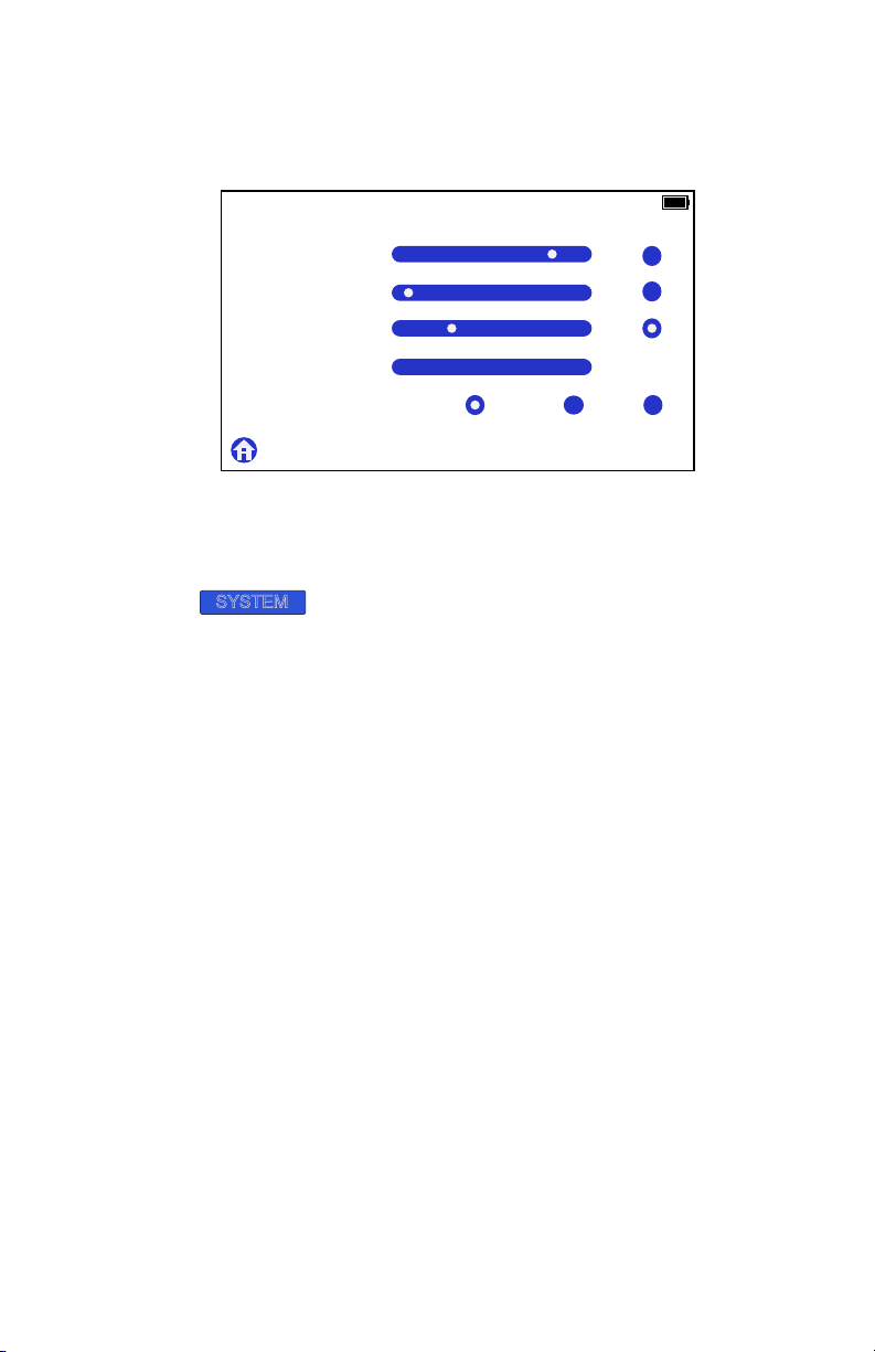
System Configuration
SYSTEM CONFIGURATION
Flashlight:
Speaker Volume:
Backlight:
RTC Date/Time:
Synchronize RTC: Input 1: Input 2: OFF:
On
On
Auto
May 01, 2016 12:34:56
100% H
SYSTEM
Choose from the five items shown in Figure 20.
Figure 20: System Configuration
1. In the Home screen CONFIGURATION menu, touch
.
2. Touch the Flashlight On button if desired. Deselect button
if not wanting the flashlight. Touch the brightness bar to
adjust the flashlight brightness.
3. Touch the Speaker Volume On button if desired, and adjust
the volume with the slider.
4. Adjust the Backlight brightness manually, or use the Auto
setting. Backlight slider does not function when Auto is selected.
5. For Real Time Clock Date/Time setting, go to page 25.
6. Synchronize RTC with Input1, Input 2 or OFF.
Choose OFF if manually setting the RTC.
23
Page 34

System Menu Notes
Flashlight
Provides brightness control and On selection. When selected ON,
the brightness slider controls the LED output. The brightness
slider has no effect if the ON button is not selected.
Speaker
Volume is similar to Flashlight, in that the slider controls the output level and “ON” turns the speaker on or off. The volume slider
has no effect if the ON button is not selected.
Backlight
Controls are manual and automatic. With Auto selected, the backlight is automatically adjusted for the ambient light. With Auto
not selected, the slider manually controls the backlight brightness.
The backlight uses the most power from the batteries.
RTC Date/Time
Set the RTC in one of two ways: (1) from an incoming timing
signal from Input 1, or Input 2, and (2) set manually. By selecting
Input 1 or Input 2, the Real Time Clock will be set automatically
when a valid time signal is connected to either input.
NOTE: For Flashlight, Speaker and Backlight: if the “ON” or
“AUTO” buttons are not selected and one of the sliders are moved,
the level is remembered and is used when the 940A is powered back
on.
24
Page 35
Manually Setting the RTC
SYSTEM CONFIGURATION
Real Time Clock
SET TIME CANCEL
Month Day Ye ar Hour Minute Second
SEP 29 2016 12 34 56
100% H
SET TIME
CANCEL
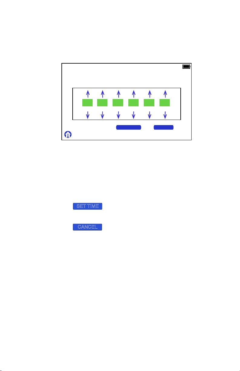
Manually adjust the Real Time Clock (RTC) from this menu. Use
the UP and DOWN arrows to change the date and time value(s)
forward or backward.
Figure 21: Set Real Time Clock Screen
1. Continued from page 23.
2. As required, touch the arrows above and below each of the
date/time selections.
3. Touch
system configuration menu.
4. Touch
thing.
to set the time/date. Returns you to the
to leave this menu without changing any-
25
Page 36
Viewing Timecodes
CONFIGURATION DISPLAY
INPUT 1 INPUT 1
INPUT 2 INPUT 2
SOURCE
SOURCE
SYSTEM
INPUT 1+2
100%
DISPLAY Functions
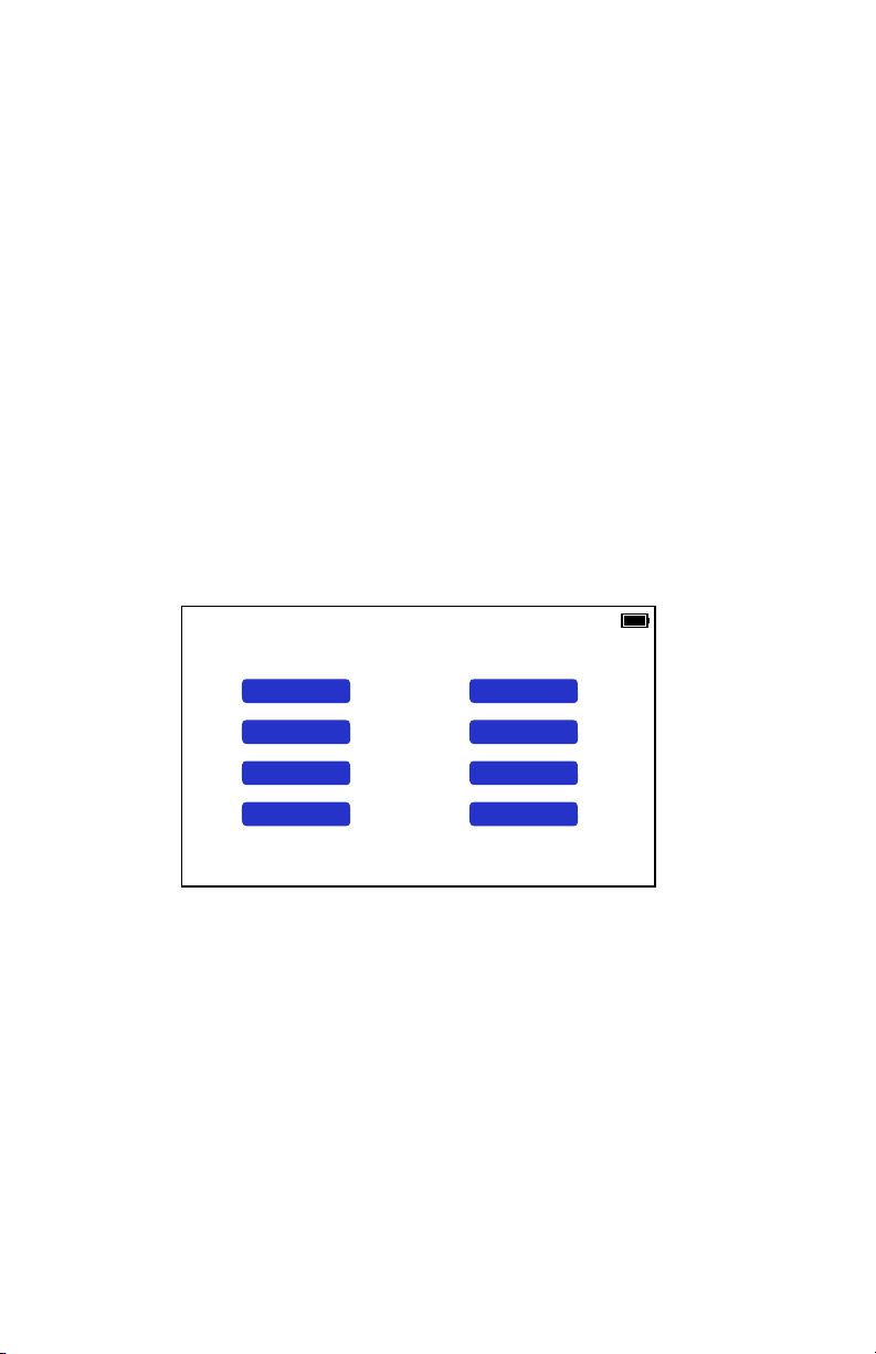
From the Home screen there are two categories: CONFIGURATION, and DISPLAY. DISPLAY allows you to view the incoming
signals from INPUT 1, INPUT 2, both Input 1 and Input 2 and
outgoing signal from the SOURCE connector.
Figure 22: DISPLAY on the Home Screen
26
Page 37
Waveform Comparisons
Start of next second
in time code
ON-TIME 1 PPS
REFERENCE
REFERENCE
IRIG ZERO
IRIG ONE
Modulated
Unmodulated
Figure 23: 1 PPS & IRIG-B Waveforms
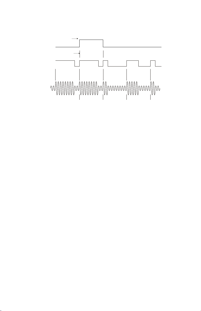
Figure 23 illustrates two of the common methods of transmitting IRIG-B, plus one pulse per second (1PPS). Unmodulated is
a square wave string of 100 bits and modulated is a 1 kHz carrier
amplitude modulated with the same number of bits.
Notice that there are three different bit widths: 8 milliseconds,
5 milliseconds and 2 milliseconds. The 8 millisecond pulse is considered a reference bit, the 5 millisecond pulse is a digital one and
the 2 millisecond pulse width is a digital zero.
Also, notice that the 1 kHz sine wave amplitude follows the
same time frame and pattern as the digital (unmodulated) signal.
27
Page 38
Unmodulated IRIG-B
INPUT 1 IRIG-B UNMODULATED
Time: 00:55:46 UTC
Date: 01 JUL 2015
DOY: 182
SBS:3346
Time Offset: 0
TQ: Locked
CTQ: <100ns
LSP: 0 LSD: 0
DSP: 0 DST: 0
PARITY: EVEN
Jitter: 0.47 uS, 0.1 RMS
In1 - In2 Delta T: ---.- uSecs
Amplitude: 4.1 Volts
Year(15) Offset(0) TQ(6)
20 40 80
P6 LSP DSP DST SIGN 1 2 4 8LSD
56 57 58 59 60 61 62 63 64 65 66 67 68 69 70
100% H
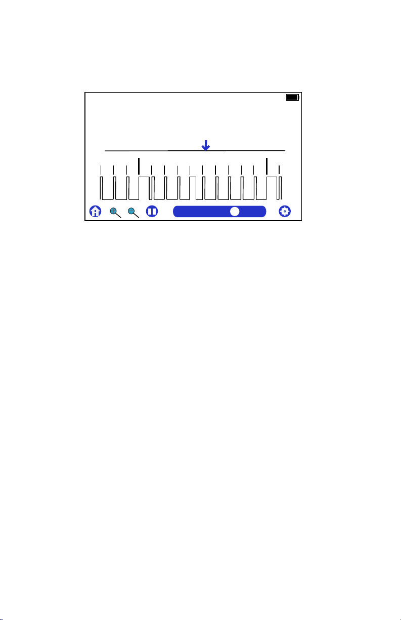
From the Home screen DISPLAY menu, press the button of the
signal you wish to view.
Figure 24: Unmodulated IRIG-B Display
The lower portion of Figure 24 graphically illustrates a part of the
unmodulated IRIG-B signal: view adjusted using the slider.
• Time/Date: UTC time; date; Day of Year; Straight Binary
Seconds (SBS); Time offset; IEEE 1344: ON or OFF.
• Time quality (TQ): Continuous Time Quality (CTQ);
Leap Second Pending (LSP); Daylight Saving change Pending
(DSP).
• Jitter, or Pulse Jitter: Two values measured and dis-
played: average jitter and rms jitter. Acceptable jitter depends on your requirement. See Figure 25.
• In1 - In2 Delta T: Time difference between the 1 PPS
signals at Input 1 and Input 2.
• Signal amplitude: Shown in Volts.
28
Page 39
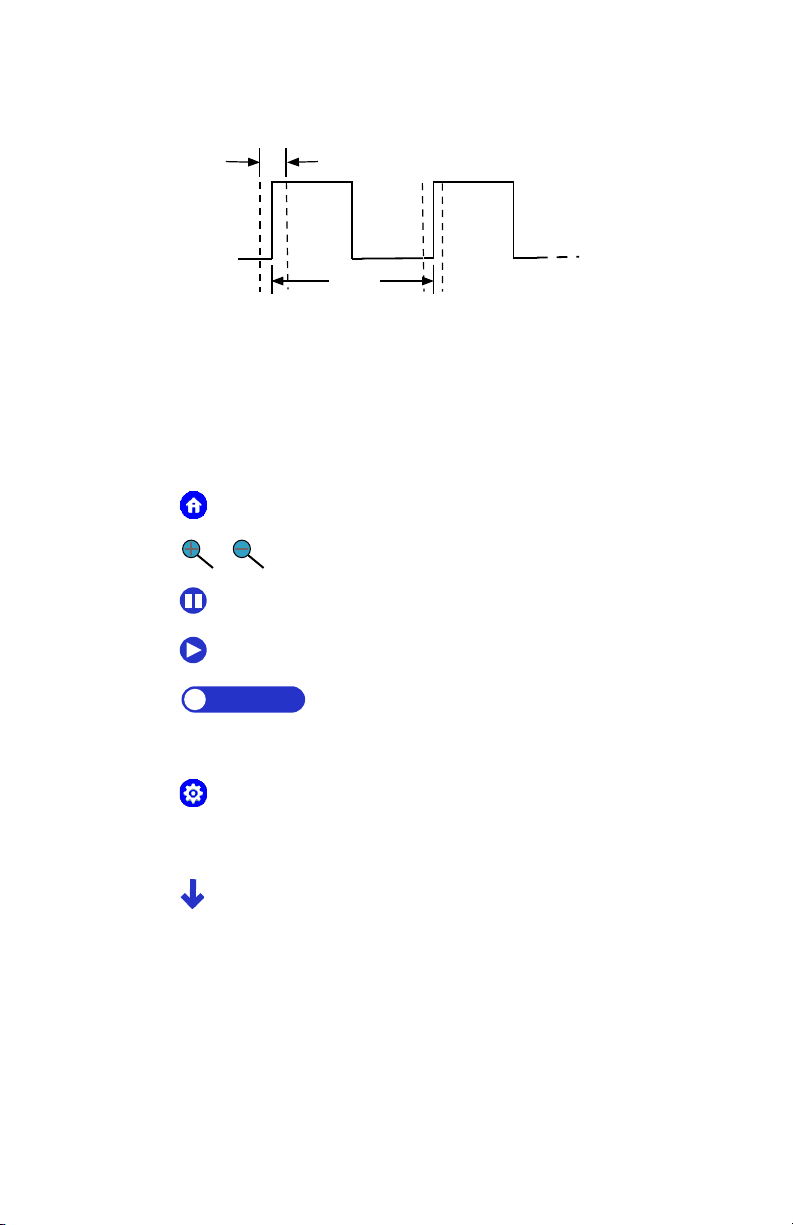
Measured Pulse Spacing
Rising Edge
Jitter
~10 ms
Figure 25: Average pulse jitter is the average difference between
the 10 ms reference and measured spacing for all 100 pulses; RMS
jitter is the calculated RMS of the difference between the 10 ms
and measured spacing for all 100 pulses.
Viewing Tools
1. – Home button: move to the Home screen.
2. – Zoom in and Zoom out.
3. – Pause: freeze the display until play is pressed.
4. – Play: resume viewing the active display after pausing.
5. – Slider bar: at the bottom of the input screen
allows you to scan through the entire range of 100 bits in the
IRIG-B time code.
6. – Gear button: at the lower right allows you to more
easily access the input configuration screen and change the
configuration.
7. – Blue down arrow over line: use to enlarge the upper
text information and lose the lower digital graphics. Touch
again to return to the split display.
29
Page 40
Modulated IRIG-B
INPUT 1 IRIG-B MODULATED
Time: 00:55:46 UTC
Date: 01 JUL 2015
DOY: 182
SBS:3346
Time Offset: 0
TQ: Locked
CTQ: <100ns
LSP: 0 LSD: 0
DSP: 0 DST: 0
PARITY: EVEN
Jitter: 0.47 uS, 0.1 RMS
In1 - In2 Delta T: ---.- uSecs
Amplitude One: 1.3 Volts
Zero: 0.7 Volts
Modulation Ratio: 2.4:1
Seconds(45)
1Pr 2 4 8
10 2 3 4
100% H
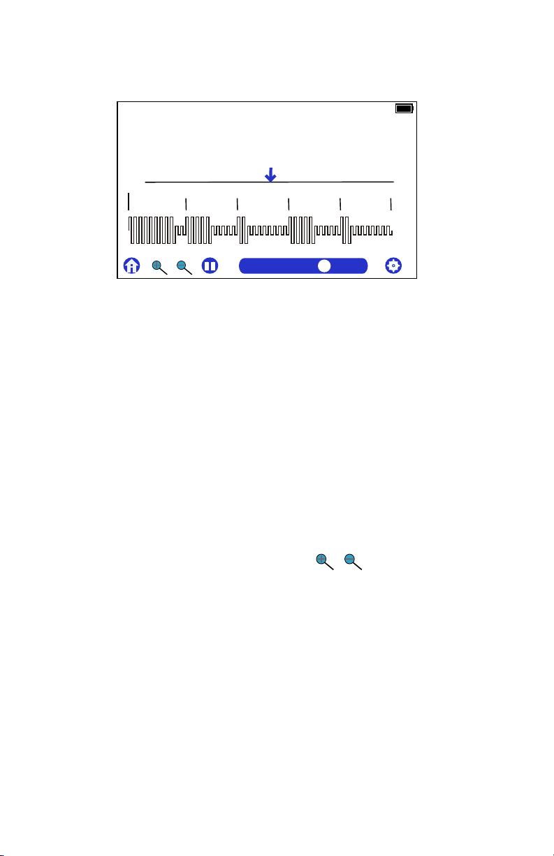
Figure 26: Modulated IRIG-B
Modulated IRIG-B carries the same time and date information as
the unmodulated, however it is not as accurate as unmodulated
IRIG-B. This is due to the difficulty in accurately measuring the
time of the 1 kHz rising wave compared to digital signal’s fast
rise time. Generally, acceptable accuracy for modulated IRIG-B is
about 10 microseconds, whereas the unmodulated accuracy can be
better than 100 nanoseconds.
In Figure 26 you will notice that the representative modulated
IRIG-B waveform is not a perfect sine wave in all magnifications.
This is because the 940A display is not able to reproduce it with
resolution. For clarity the individual bits in the IRIG string are
shown as a modified square wave, whereas the text above the waveform indicates accurate values. The analog waveform will appear
more correctly as you zoom in using the zoom tool.
30
Page 41
Input 1 PPS Timing
INPUT 1 ONE PULSE PER SECOND
Pulse Width: 10.0 mSecs
Jitter: ---.- uS, ---.- RMS
In1 - In2 Delta T: ---.Amplitude: 4.8 Volts
100% H
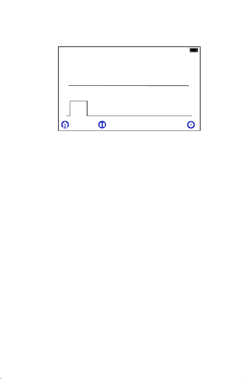
Figure 27: 1 PPS Signal Connected to Input 1
The 1 PPS signal is generally a 10 millisecond pulse that occurs
every second, with the rising edge on time. Synchronization between the 1 PPS and IRIG-B time code can be seen in Figure 23.
A 1 PPS signal connected to Input 1 would display as illustrated
in Figure 27.
31
Page 42
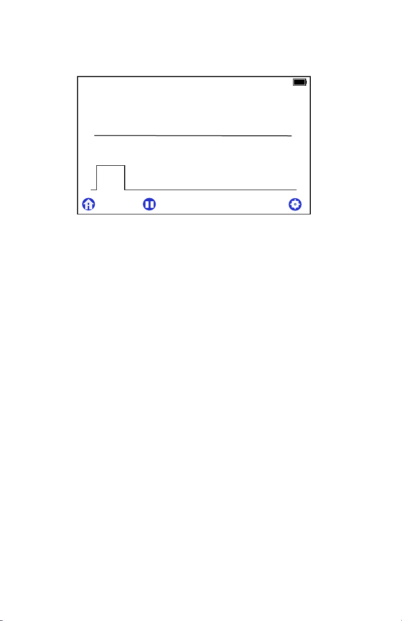
Source 1 PPS Timing
Source ONE PULSE PER SECOND
Pulse Width: 10.0 mSecs Amplitude: 5 Volts
Load: 0 mAmps
100% H
Figure 28: 1 PPS Signal at Source Connector
The 1 PPS signal is generally a 10 millisecond pulse that occurs every second, with the rising edge on time. Synchronization
between the 1 PPS and IRIG-B time code can be seen in Figure 23.
A 1 PPS signal transmitted from the source connector would display as illustrated in Figure 28.
32
Page 43
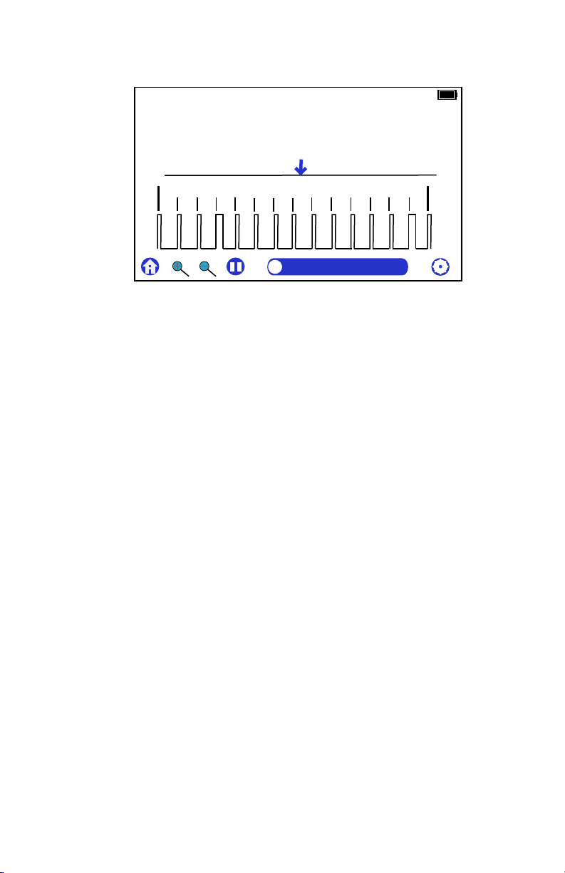
DCF77 Timing
INPUT 2 DCF77
Time: 08:20:08
Date: 06 OCT 2016
DOW: Thu
Z1: 1 Z2: 0
A1: 0 A2: 0
Jitter: ---.- uS, ---.- RMS
In1 - In2 Delta T: ---.- uSecs
Amplitude: 4.8 Volts
0 1 2 3 4 5 6 7 8 9 10 11 12 13 14
100% H
Figure 29: DCF77 Signal Connected to Input 2
DCF77 is a one minute time code with 58 bits of time information. The 59th second bit is missing, which is normal for standard
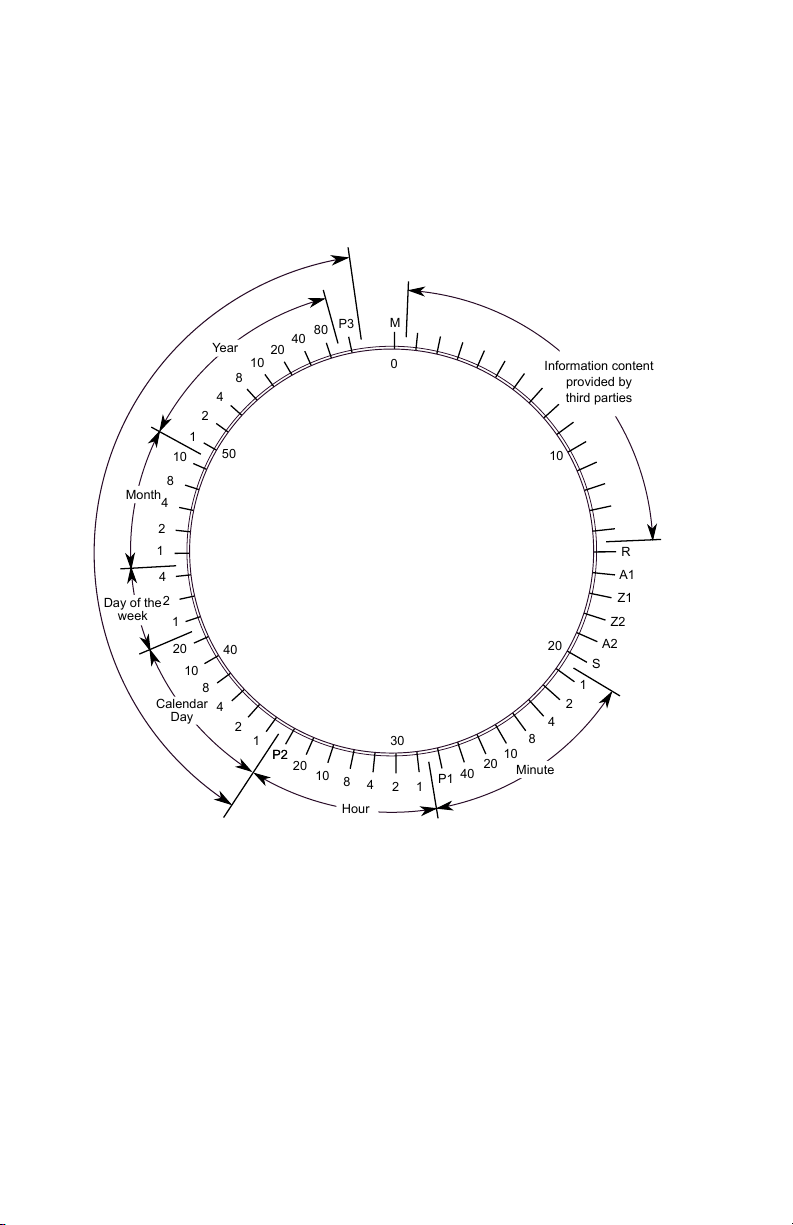
DCF77. It can be illustrated as an analog clock as seen in Figure 30.
DCF77 Marker Details – Figure 30
M: minute marker (second marker No. 0): 0.1 s
R: second marker No. 15 indicates service request to the DCF77
signal generation system
A1: announcement of a forthcoming change from CET to CEST
or vice versa
Z1, Z2: time zone indication: CET: Z1, 0.1 s, Z2 0.2 s; CEST: Z1
0.2 s, Z2 0.1 s
A2: announcement of a leap second, 0.2 s
S: Start of encoded time. Always 1.
P1, P2, P3: parity check bits
DCF77 Time Zone Arrangement
• CET is Central European Time, UTC + 1:00
• CEST is Central European Summer Time, UTC + 2:00.
33
Page 44
Minute
Hour
Information content
provided by
third parties
Year
Month
R
A1
Z1
Z2
A2
S
1
2
4
8
10
20
40
P1
12
4
8
10
20
P2
1
2
4
8
10
20
1
2
4
Day of the
week
Calendar
Day
1
2
4
8
10
1
2
4
8
10
20
40
80
P2
P3
M
0
10
20
30
40
50
Figure 30: DCF77 Signal Elements show as a 60 second clock.
Time and marker details are seen around the circumference of the
circle. The 59th second bit is missing for Standard DCF77.
34
Page 45

Specifications
INPUTS
Connectors Two BNC
Signals IRIG-B (modulated, unmod-
ulated, modified Manchester),
DCF77, 1 PPS
Levels 25 Vpk, maximum
Impedance Selectable: high impedance, 50
ohms or 100 ohms.
OUTPUT
Connector One, BNC
Signals IRIG-B (modulated, unmodu-
lated), DCF77, 1PPS
Levels 1 – 15 Vdc, 1 – 10 Vpk
Drive 125 mA @ 5V
Time Ref. Input 1, Input 2, Real Time
Clock, or Custom
SYSTEM
Display 800 x 480 color TFT capacitive
touchscreen, backlit
Single or Dual Timing Signals
Data and/or Waveform
Reference Input 1, Input 2 or Custom
Features
Flashlight Built in LED
Audio Indicator tone (enable/disable)
35
Page 46

POWER
Battery
Type Li-ion (9000 mAh capacity)
Operation 24 hours, typical
Charge 8 – 12 hours with unit off
External
Voltage +5 Vdc
Current 1 A
Cable 24 AWG Required
Connector USB Micro-B
GENERAL
Physical
Size 204.7 x 166.5 x 48.5 mm
(8.1 x 6.6 x 1.9 in.)
381 x 305 x 229 mm, shipping
(15 x 12 x 9 in.)
Weight 0.6 kg (1.4 lbs), maximum
2.5 kg (5.5 lbs), shipping
Environ.
Temperature Operating: -10oC to +50oC
Charging: 0oC to +45oC
Nonoperating: -40oC to +75oC
Humidity Noncondensing
36
Page 47
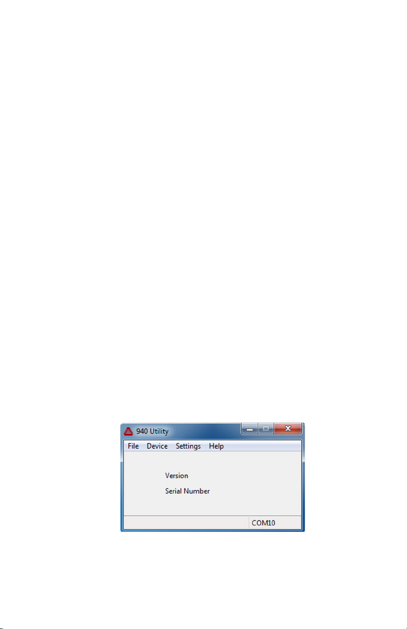
The 940A Utility
Updating Firmware
This section describes how to update the firmware on your Model
940A. Check the Arbiter web site, or contact Arbiter Systems technical support, for information on firmware updates.
Firmware Package
Note that the new firmware will be in zipped format and does not
need to be unzipped (or unpacked) before uploading to the 940A.
The Utility will unpack the required files when necessary.
Driver Software
The 940A Utility software package includes the driver and the operation manual.
Updating the 940A
1. Power on the 940A and start the 940A Utility. See Figure 31.
Figure 31: 940A Utility Opening
37
Page 48
2. Connect the supplied Micro USB cable between the USB 2.0
port on the 940A and the computer.
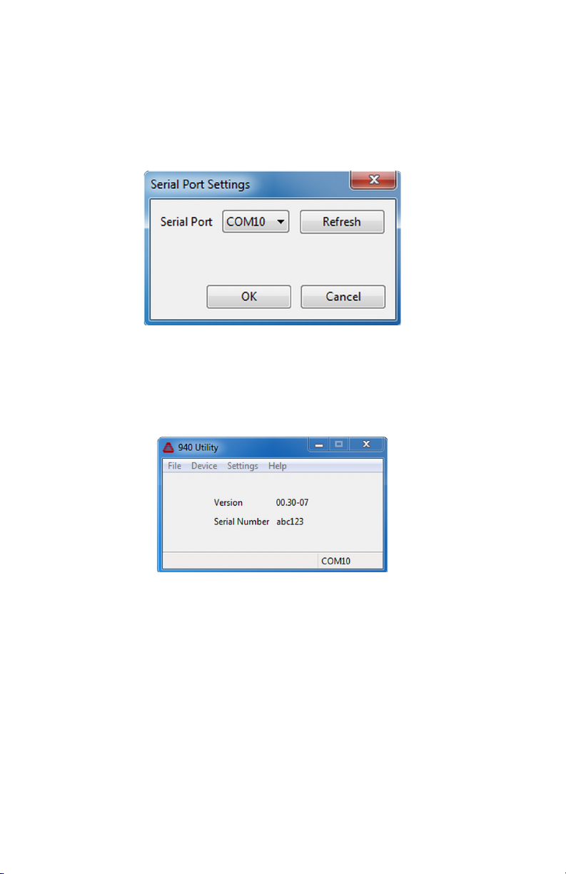
3. To select the COM port, click Settings then Serial Port
in the Utility menu. Select the COM port of your computer,
click OK. See Figure 32.
Figure 32: Selecting COM Port
4. The Utility should then read and display the current firmware
version and the serial number. See Figure 33
Figure 33: 940A Utility Reading Serial Number
5. In the 940A Utility main menu click Device then Upload
Firmware; browse to the location of the new firmware, select
the zipped file and click Open.
6. Click the Upload To Device button. A progress bar will
appear that counts the number of blocks loaded and the total.
7. After the upload, the 940A should restart and pause on the
startup screen. A message in the startup screen should ap-
38
Page 49
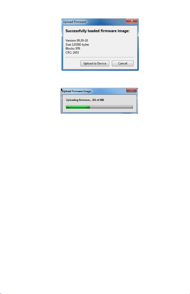
Figure 34: 940A Firmware Ready to Upload
Figure 35: 940A Upload Progress
pear regarding the success of the upload and the new firmware
version from the 940A.
8. On the 940A Utility you can also select Device, Read, and it
should read the firmware version.
9. Touch the 940A display itself to leave the startup screen.
39
Page 50
IRIG-B Information
IRIG Time Code Formats
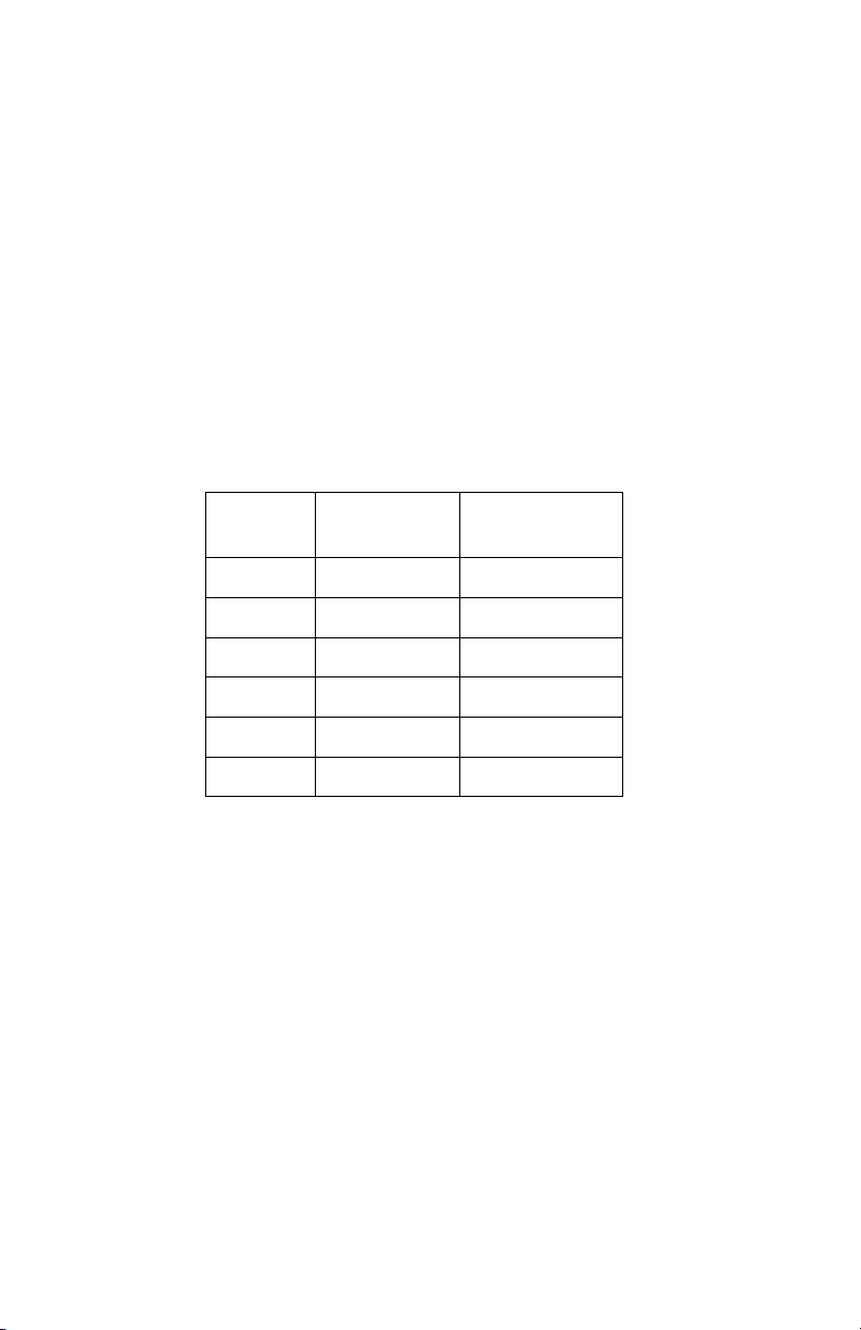
Listed below are the various formats in the IRIG specification.
Arbiter clock products produce Format B.
Format Pulse Rate Index Count
Interval
IRIG-A 1000 PPS 1 ms
IRIG-B 100 PPS 10 ms
IRIG-D 1 PPM 1 minute
IRIG-E 10 PPS 100 ms
IRIG-G 10000 PPS 0.1 ms
IRIG-H 1 PPS 1 second
Table 2: Various IRIG Time Code Formats
Time Code Attributes
All IRIG time code formats use pulse-width coding. A ”binary
1” pulse has a duration of 50% of the index count interval (see
Table 2); a ”binary 0” pulse has a duration of 20% of the index
count interval; pulse identifiers have a duration of 80% and used
as reference markers.
IRIG-B time code signals may be either Unmodulated or Modulated. Unmodulated time codes are DC level shift with no carrier
signal. Modulated time codes are amplitude-modulated, sine wave
carrier. For IRIG-B, the carrier is 1 kHz.
40
Page 51

Encoding
IRIG-B consists of 100 bits produced every second, 74 bits of which
contain various time, date, time changes and time quality information of the time signal. It consists of logic ones, zeros and position
identifier bits. There are three functional groups of bits in the
IRIG-B time code: Binary Coded Decimal (BCD), Control Functions (CF) and Straight Binary Seconds (SBS).
The BCD group contains time information including seconds,
minutes, hours, days and year, and recycles yearly. It reads zero
(0) hours at 2400 hours each day and day one (1) on day 365 at
hour 2400. BCD year counts two-digit year and cycles to the next
year on January 1st, and counts to 2099 (99).
The CF (Control Function) group contains year, time quality,
leap year, pending leap seconds and parity. More recently, Continuous Time Quality (CTQ) was added according to IEEE C37.118-
2011.
SBS (Straight Binary Seconds) counts time of day in seconds,
recycling daily, reading zero (0) at 2400 each day.
IRIG-B Bit Assignments
Nomenclature
BCD = Binary Coded Decimal; CF = Control Functions; SBS =
Straight Binary Seconds; TQ = Time Quality; CTQ = Continuous
Time Quality
41
Page 52
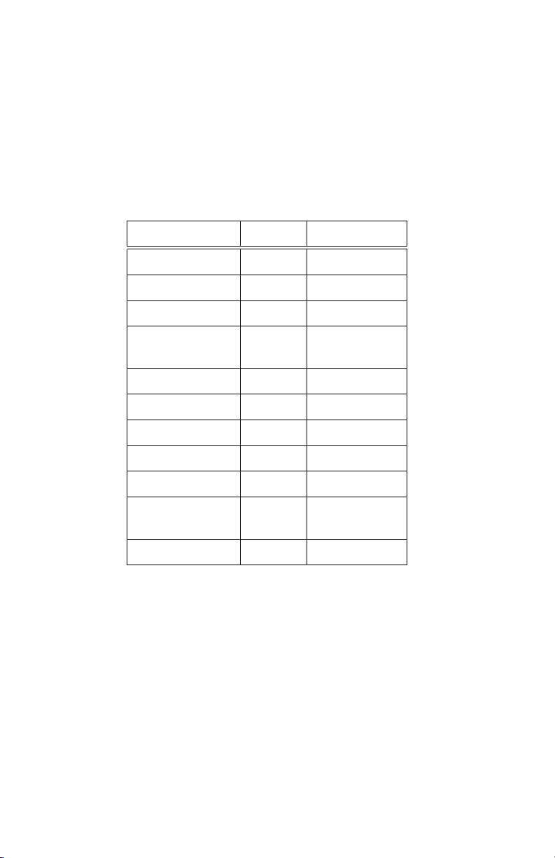
Code Group Bits Includes
BCD Seconds 0 to 8 Ref. bit at 0
BCD Minutes 9 to 18 Ref. bit at 9
BCD Hours 19 to 28 Ref. bit at 19
BCD Days 29 to 48 Ref. bit at 29
7 index bits
BCD Year 49 to 58 Ref. bit at 49
CF, Offset 59 to 68 Ref. bit at 59
CF, TQ 69 to 74 Ref. bit at 69
CF, Parity 75 –
CF, CTQ 76 to 78 –
SBS, 86400 secs 79 to 98 Ref. bit at 79
one index bit
Reference bit 99 –
Table 3: IRIG Time Code Bit Assignments
FONKEL ME
XICANA
Tel: (55) 55 33 61 14
informes@fonkel.com.mx
www.fonkel.com.mx
42
 Loading...