

Page 1
Apple A4 Teardown
Apple A4 Teardown
Step 1 -
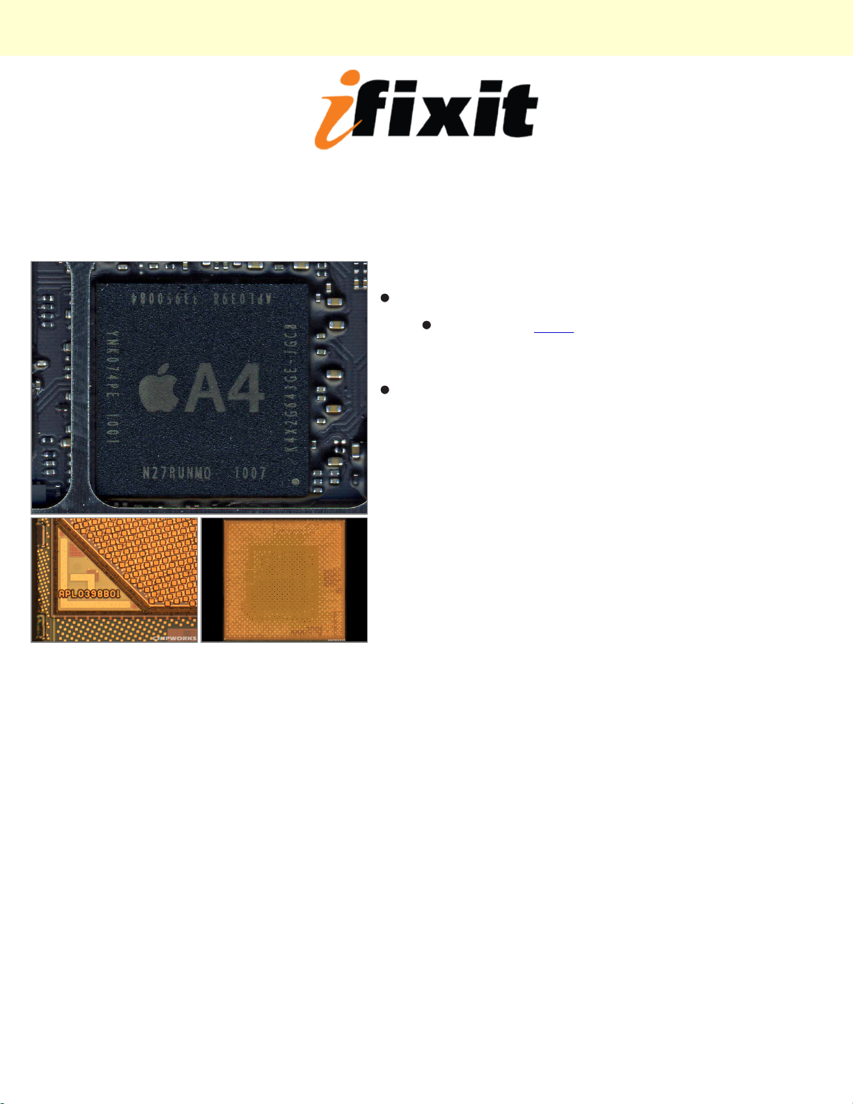
Apple's A4 microprocessor is the brain of the iPad.
The silkscreen on the A4 reads N26CGM0T APL0398
339S0084 YNL215X0. But that's not very
interesting—those numbers don't mean much to us,
either. Let's see what we can find inside.
The A4 is an ARM processor featuring packageon-package construction to improve the speed
and efficiency of internal processes.
© 2010 iFixit — CC BY-NC-SA www.iFixit.com Page 1 of 16
Page 2
Apple A4 Teardown
Step 2
Back when the original iPhone came out, we worked
with some friends of ours in Silicon Valley to dissect the
processor. The equipment we used wasn't nearly as
cutting-edge as what Chipworks has, but it got the job
done.
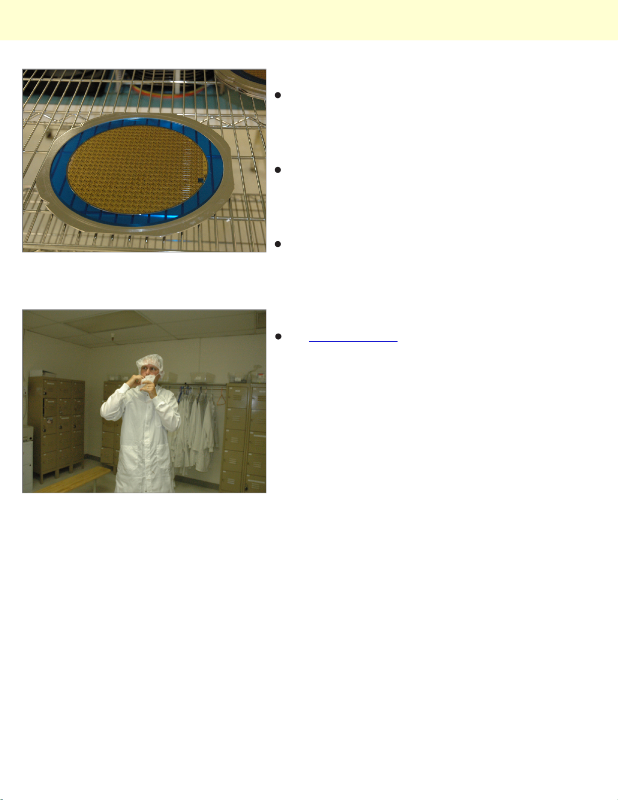
This is a silicon wafer. Each small square is a chip,
called a die. The processor die in the A4 is 7.3 mm on
each side, for a 53 square mm total area. The percent
of working dies that you can get from a wafer like this is
called the yield.
The A4 is actually much more than just a processor— it
's a Package on Package, or PoP. In fact, there are
three silicon dies inside the A4!
Step 3
Our illustrious leader preparing to enter a cleanroom for
some silicon surgery on the original iPhone.
© 2010 iFixit — CC BY-NC-SA www.iFixit.com Page 2 of 16
Page 3
Apple A4 Teardown
Step 4
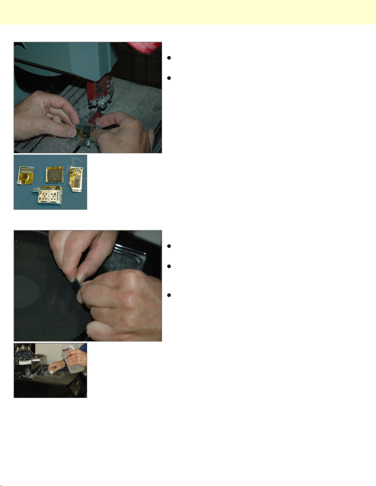
You have to first remove the processor from the main
board before dissecting it.
There are only two ways to remove a processor from a
circuit board: Extreme force and extreme heat. Guess
which approach we used?
Step 5
Next, cut the processor in half to take a cross-section
photo.
Band saws are much too crude for this, so we actually
grind through the processor slowly, taking off very small
amounts of material as we go.
You can see why it can be tough to take a clear, solid
photo of a package's cross-section. The processor is
actually one of the larger packages in the iPhone, and
still very finicky to handle. Imagine trying to do this with
a package a tenth of its size.
© 2010 iFixit — CC BY-NC-SA www.iFixit.com Page 3 of 16
Page 4
Apple A4 Teardown
Step 6
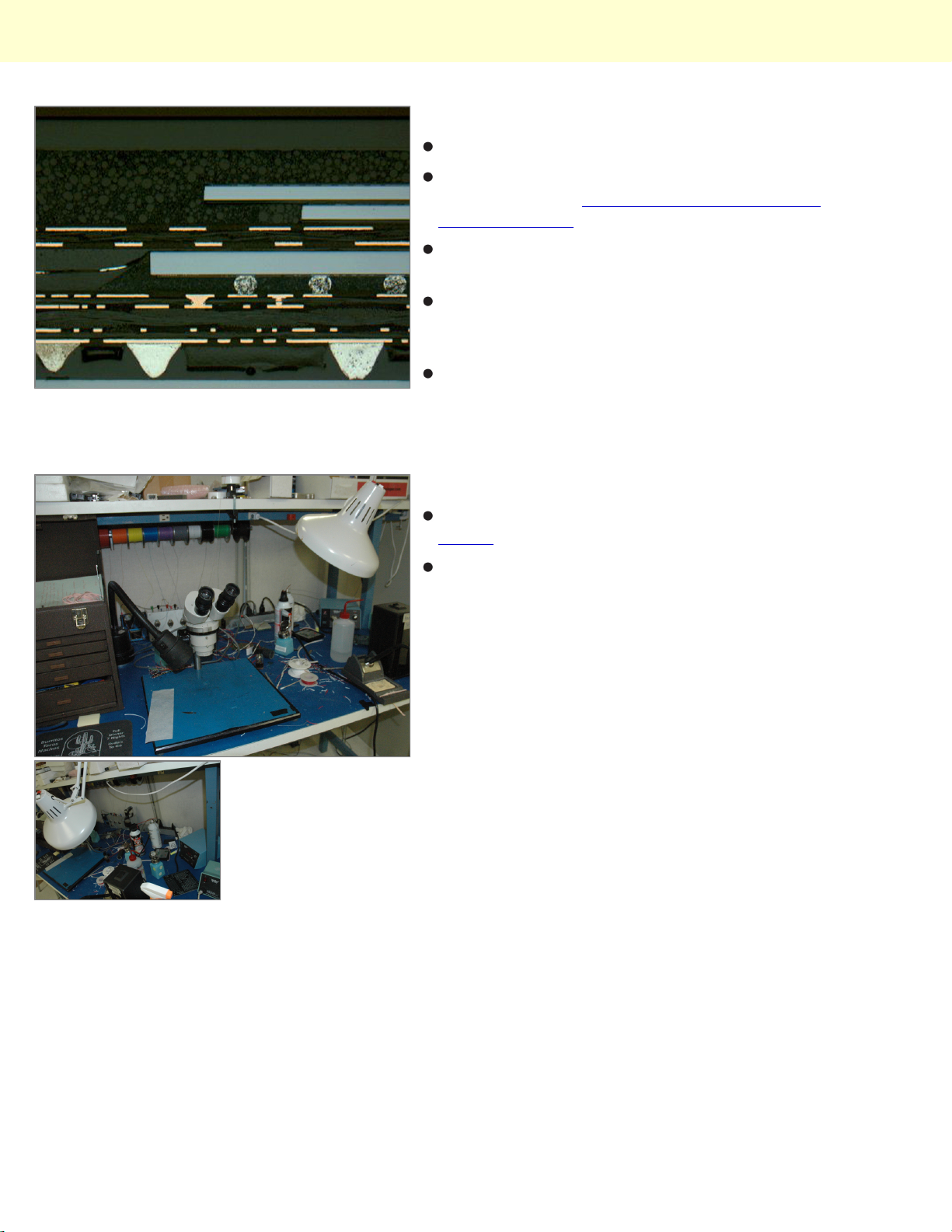
So what is a package? You're looking at one.
This is a cross-section of the iPhone's ARM processor
+ RAM package. Click here to see it in its full,
2854x313 glory.
The processor itself is the center rectangle. The silver
circles underneath it are solder balls.
The two rectangles above the processor are RAM dies.
They are offset from each other to make room for the
wirebonds, which you can't see in this shot.
Having the RAM so close to the processor both
reduces latency—making RAM access faster—and cuts powe
r consumption, helping your battery last longer.
Step 7
This is our friend's workbench. We're also huge fans of
Weller.
These are the the types of tools that'd make MacGyver
proud... Although we suspect that all he'd need is a
paperclip and two strips of duct tape to take apart the
processor.
© 2010 iFixit — CC BY-NC-SA www.iFixit.com Page 4 of 16
Page 5
Apple A4 Teardown
Step 8
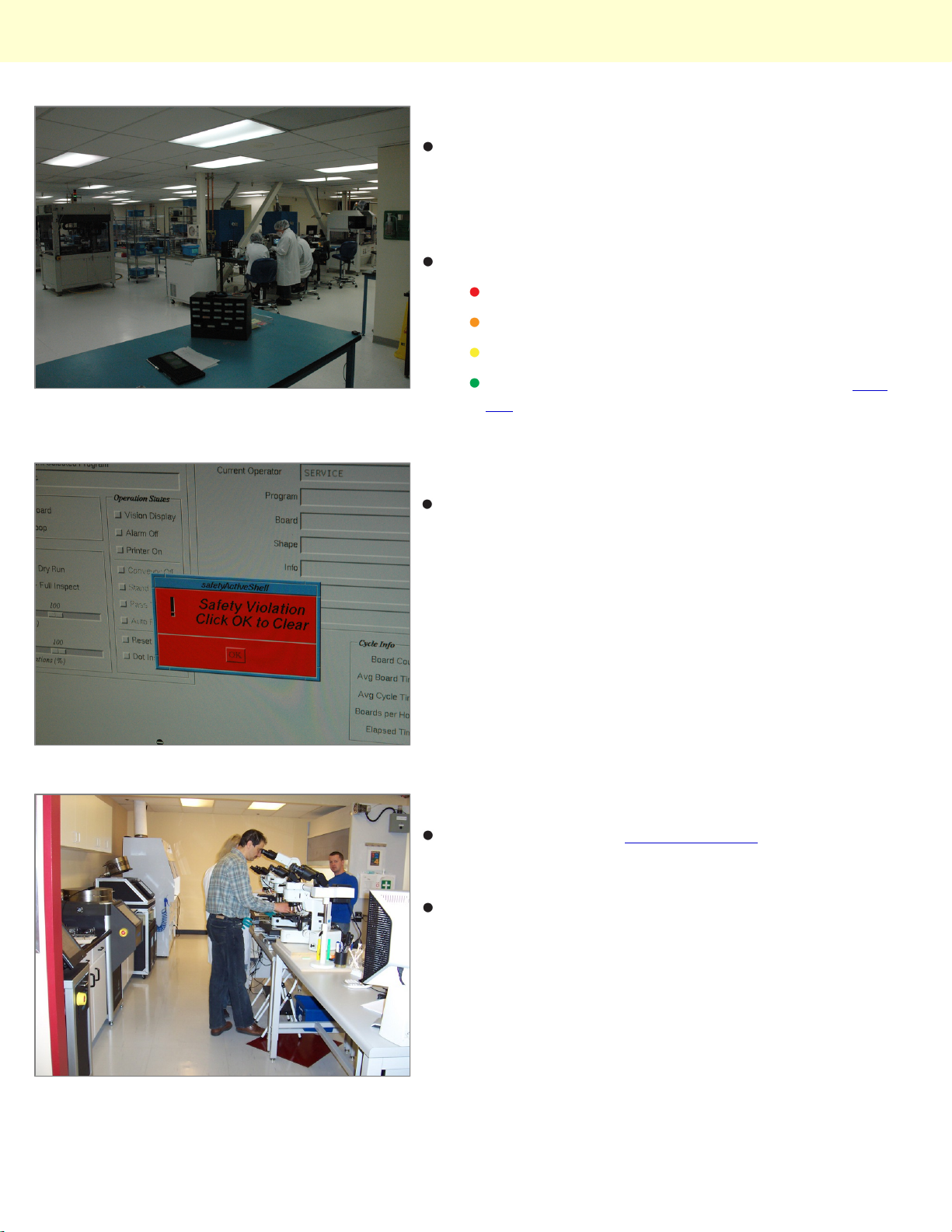
This is a typical cleanroom. Regular people—people wh
o might even shop at the same supermarkets as
you—suit up every day and go to work in rooms like th
ese. It's absolutely imperative to keep dust, lint, and
hair away from the task at hand.
Tools of the trade:
Step 9
If only all safety violations were this easy to fix!
Scanning electron microscopes
High resolution X-ray machines
Really big magnifying glasses and microscopes
A number of other gadgets you might find in Q's
lab
Step 10
Chipworks is based in Ottawa, Ontario. It gets so cold
there that your tires can actually crack if you're not
careful.
The equipment at Chipworks is quite different than
you'll find in most semiconductor facilities. Every single
machine they have exists with one purpose in mind:
discovering what's inside the latest chips.
© 2010 iFixit — CC BY-NC-SA www.iFixit.com Page 5 of 16
Page 6
Apple A4 Teardown
Step 11
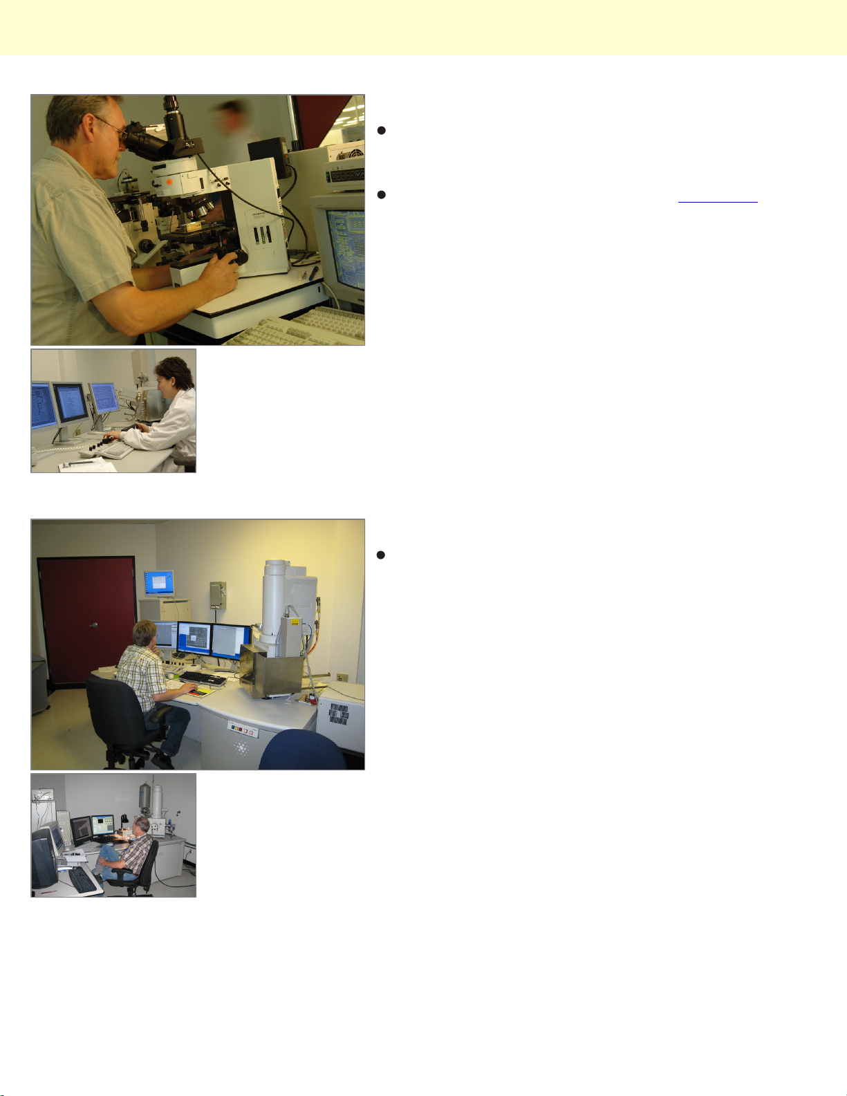
Microscope analysis, both of the optical and SEM kind.
Either one is definitely not your typical community
college biology lab unit.
Precision matters in this business, and Chipworks is
known to be very precise.
Step 12
A scanning electron microscope (SEM) in action. These
are just some of the tricks up Chipworks' sleeve. The
SEM is able to see hundreds of times more detail than
an optical microscope.
© 2010 iFixit — CC BY-NC-SA www.iFixit.com Page 6 of 16
Page 7
Apple A4 Teardown
Step 13
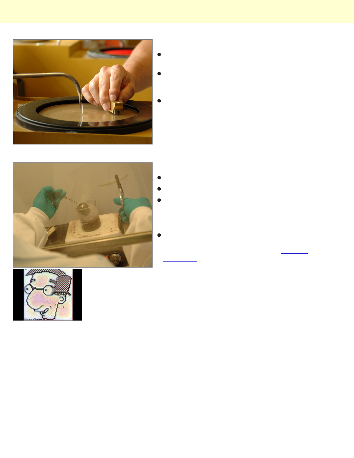
Grinding down a package. Keeping the part level as
you grind is critically important.
This process is incredibly painstaking. There's actually
a fine art in grinding to exactly the right spot for the
photo while keeping the surface perfectly level.
We (at iFixit) are terrible at this. That's why we shipped
our iPad to Chipworks.
Step 14
The next step is to remove the outer packaging.
Tea time? Nope, just time for a nice acid bath.
Dipping the processor in acid dissolves the ceramic
packaging containing the silicon. Using the appropriate
concentration of acid for the type of ceramic packaging
is critical.
Every once in a while, looking at a die yields nifty
surprise hidden by the manufacturers. Alas, Milhouse
was not found in the iPad. But he was recently
discovered inside a Silicon Image chip!
© 2010 iFixit — CC BY-NC-SA www.iFixit.com Page 7 of 16
Page 8
Apple A4 Teardown
Step 15
Alright, now you know how we did it. But what does the
A4 look like inside?
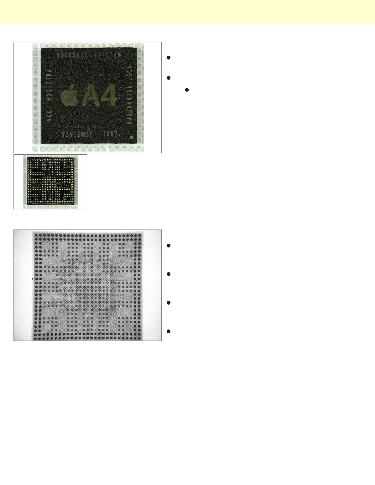
Photos of the top and bottom of the A4 package.
Those tiny dots you see on the underside are
solder balls that adhere the processor to the logic
board. They transmit all power, grounding, and
information to-and-from the processor and board.
Step 16
Before dismantling it, Chipworks took an X-ray image of
the A4 processor to get a feel for how things are laid
out inside.
If you look closely, you can see hundreds of thread-like
interconnects (wirebonds) that carry electronic signals
between dies.
The A4 has three layers: Two layers of RAM (Samsung
K4X1G323PE), and one layer containing the actual
microprocessor.
This Package-on-Package construction gives Apple the
flexibility to source the RAM from any manufacturer
they want—they're not locked into Samsung.
© 2010 iFixit — CC BY-NC-SA www.iFixit.com Page 8 of 16
Page 9
Apple A4 Teardown
Step 17
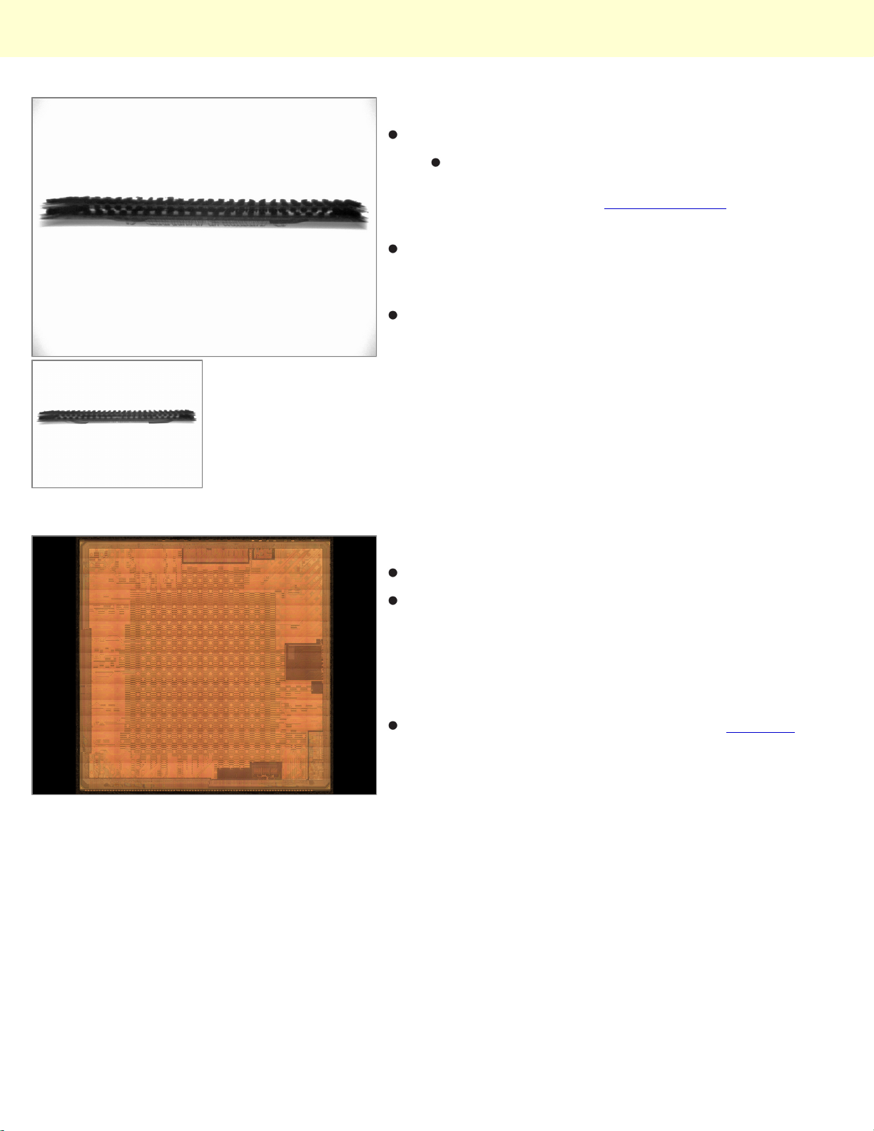
Here are two side X-rays of the A4 processor.
These pictures are shot at two focal points across the
width of the processor. They were quick shots, so we
apologize if they're a little fuzzy.
The DRAM in the A4 is made by Samsung, so
wirebonds are coming from both sides—unlike other DR
AM modules Chipworks has seen from other
manufacturers.
The dark dots along the inside of the processor
are solder balls connecting the dies together.
These are known as Ball Grid Arrays (or BGAs) in
the industry.
Step 18
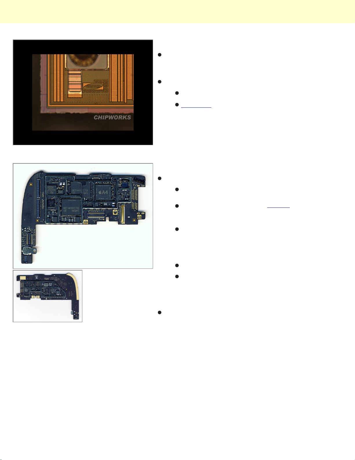
This is a die metal 8 layer.
Every iPhone processor that we have dissected has
had a Samsung part number on the processor die. We
have not found any Samsung markings on the A4
(outside of the DRAM), perhaps the clearest sign to
date that Apple is in firm control of the semiconductor
design.
We don't expect to find any markings from PA Semi,
Apple's recent acquisition, but it's safe to assume they
played a major role in designing this package.
© 2010 iFixit — CC BY-NC-SA www.iFixit.com Page 9 of 16
Page 10
Apple A4 Teardown
Step 19
This is the SDRAM inside the A4. Yes, that's a
Samsung logo. No, that doesn't mean Samsung
designed the A4—just the RAM.
Samsung's 1 Gb mobile DDR SDRAM (x2)
The part number on each die is K4X1G323PE.
Decoding this part number shows there is 2Gb of
memory inside. This translates into ~128MB of
memory per die, for 256 MB total.
Step 20
So now that we've seen the inside, what can we conclude?
There's not much revolutionary here. In fact, the A4 is quite
similar to the Samsung processor Apple uses in the iPhone.
It's clear from both hardware and software that this is a
single core processor, so it must be the ARM Cortex A8,
and NOT the rumored multicore A9.
It's quite challenging to identify block-level logic inside a
processor, so to identify the GPU we're falling back to
software: early benchmarks are showing similar 3D
performance to the iPhone, so we're guessing that the iPad
uses the same PowerVR SGX 535 GPU.
The iPad has 256 MB RAM, same as the iPhone.
The A4 sips power. In fact, power consumption is probably
the reason Apple hasn't stepped up performance much from
the iPhone. In order to get 10 hours of battery life, the entire
iPad (including display) has to pull less than 2.5 Watts on
average.
That's it for the A4. Let's take a look at some of the other chips
inside the iPad.
© 2010 iFixit — CC BY-NC-SA www.iFixit.com Page 10 of 16
Page 11
Apple A4 Teardown
Step 21
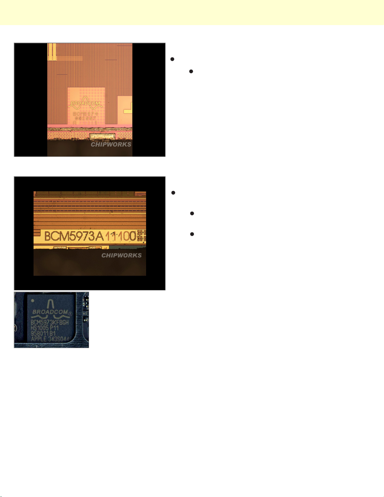
Capacitive touchscreen controller.
Step 22
Broadcom's I/O microcontroller with NVM (used for
touchscreen)
Broadcom BCM5974
Broadcom BCM5973KFBGH HS0951P11 952280
B1
Apple 343S0446
© 2010 iFixit — CC BY-NC-SA www.iFixit.com Page 11 of 16
Page 12
Apple A4 Teardown
Step 23
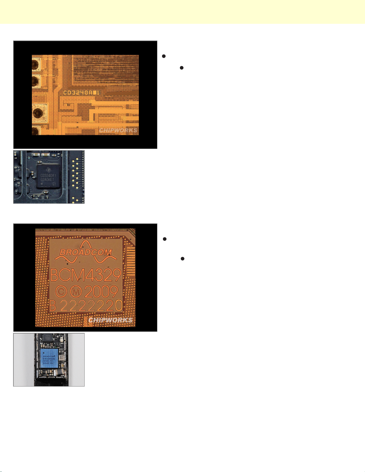
The Texas Instruments touchscreen line driver.
CD3240A 01D5AKT G1
Step 24
Broadcom 802.11a/b/g/n WiFi + Bluetooth 2.1 + EDR
and FM.
Broadcom BCM4329XKUBG CD1004 P21
© 2010 iFixit — CC BY-NC-SA www.iFixit.com Page 12 of 16
Page 13
Apple A4 Teardown
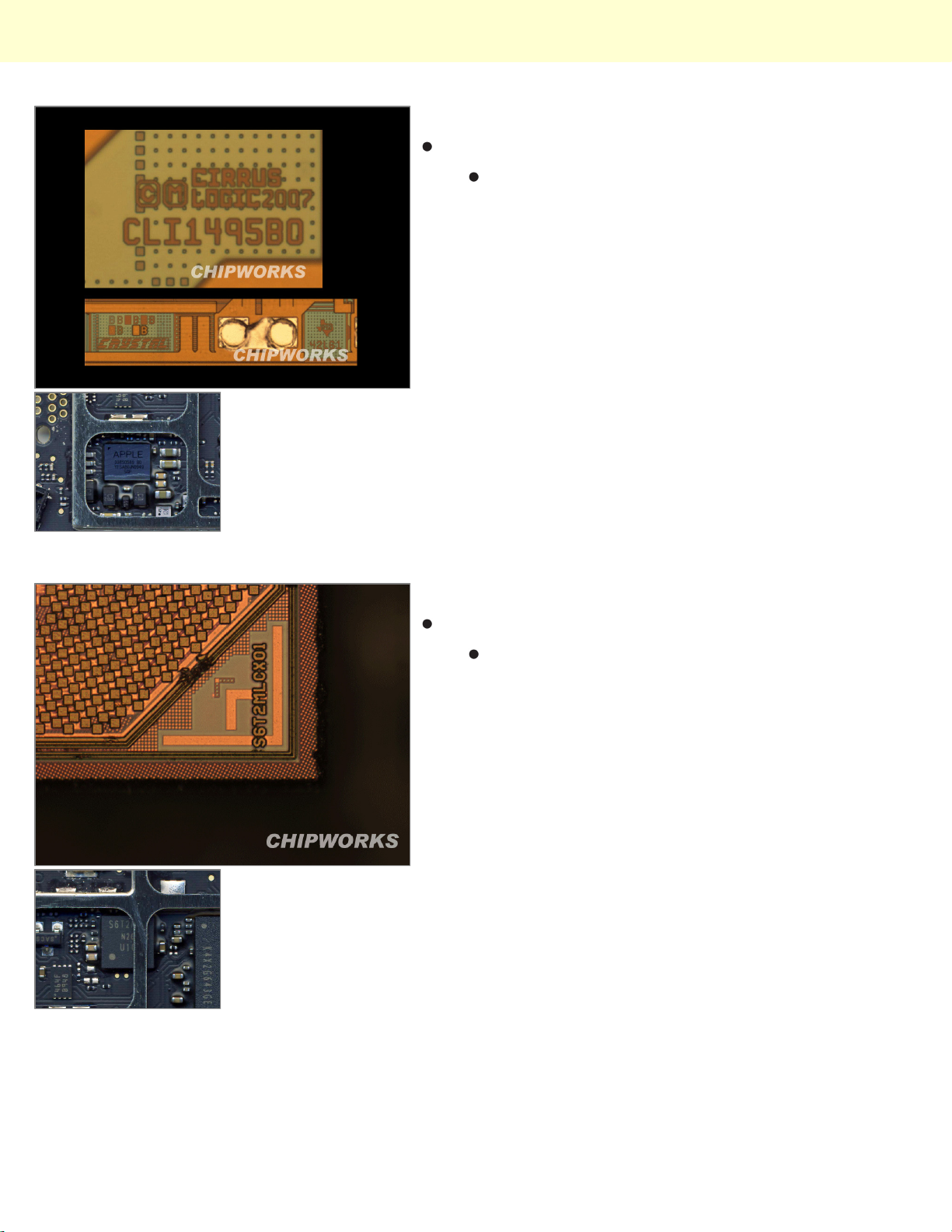
Step 25
Cirrus Logic device – suspected audio processor.
Apple 338S0589 B0 YFSAB0PY1001
Step 26
Suspected power management.
S6T2MLC N2266XQT U1003 A1
© 2010 iFixit — CC BY-NC-SA www.iFixit.com Page 13 of 16
Page 14

Apple A4 Teardown
Step 27
Mux/demux part for DisplayPort and PCIe connections.
NXP L0614 01 37 ZSD950
Step 28
Display.
LG SW0627B 01SWL-0032C 1003 N23977ON
© 2010 iFixit — CC BY-NC-SA www.iFixit.com Page 14 of 16
Page 15
Apple A4 Teardown
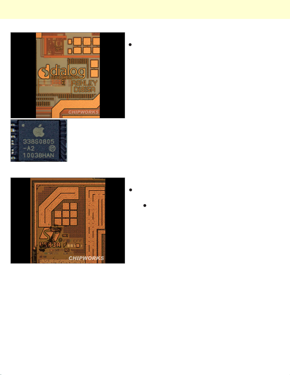
Step 29
Apple 338S0805 A2 e1 10028HBB
Step 30
Accelerometer (confirmed by die markings of ASIC and
MEMS device) - STM-LIS331DLH.
STMicroelectronics 2949 33DH OK2 CL
© 2010 iFixit — CC BY-NC-SA www.iFixit.com Page 15 of 16
Page 16
Apple A4 Teardown
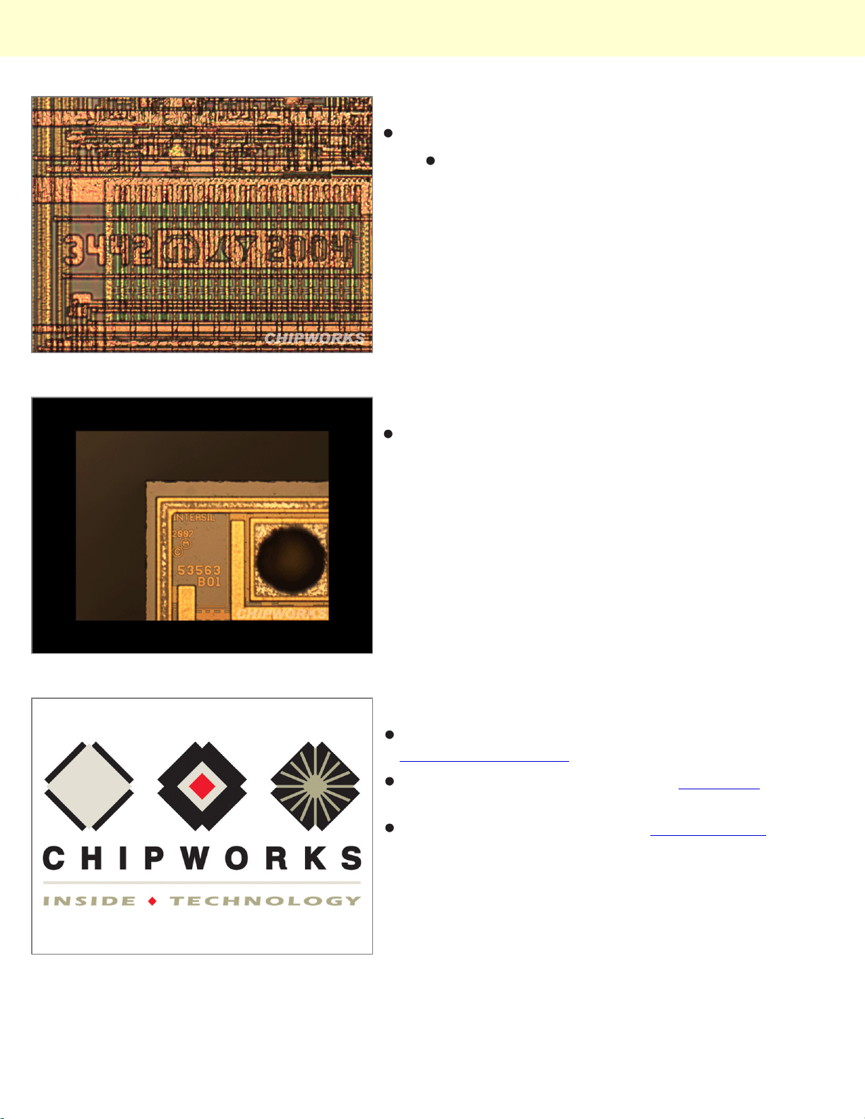
Step 31
DC-DC regulator.
Step 32
Intersil i976 45AIRZ F95OHX
Linear Technologies 3442 N7667 LT9L
Step 33
That's what we've got so far. We'll add more photos as
Chipworks posts more.
We'd like to thank our friends over at Chipworks for
their exceptional work.
Don't forget to take a peek at our iPad Teardown for a
complete disassembly.
© 2010 iFixit — CC BY-NC-SA www.iFixit.com Page 16 of 16
 Loading...