

Page 1

iPad FCC Teardown
iPad FCC Teardown
Update 4/3
We have taken apart a production iPad, with much higher resolution photos.
FCC Photo Analysis
The FCC was kind enough to show the internals of the WiFi iPad before it was released! The photos
that they put up had the interesting bits hidden behind grey squares, but we were able to extract the
raw files! The WiFi iPad is officially Apple model A1219, while the 3G iPad is A1337.
Apple requested this information stay concealed until August 17th. Clearly, the FCC ignored them.
Note: This is not a traditional iFixit teardown. These photos are not up to our normal quality standards,
and it's quite difficult to perform analysis on the low-resolution files. We will be doing a real teardown
of the iPad on April 3, the moment we get our pre-ordered units.
Update: 3G iPad
We have uncovered internal photos of the 3G iPad, which won't be released for at least a month!
Starting at step 14.
Just want the highlights? Stay tuned to @ifixit for news as we unveil it.
© 2010 iFixit — CC BY-NC-SA www.iFixit.com Page 1 of 10
Page 2
iPad FCC Teardown
Step 1 -
Performing analysis as we go. Please help out in the
comments! To see highest resolution files, log in and
you'll get a large option on each photo.
One word of caution: This is likely a preproduction
board, and Apple very well may have changed some
suppliers since they gave the FCC a sample unit. Take
this data with a grain of salt until we are able to analyze
a production model tomorrow.
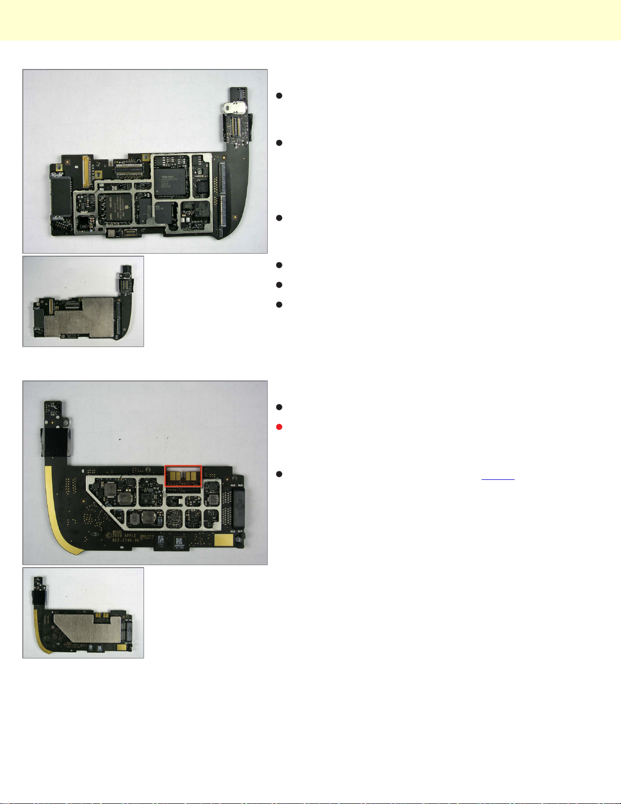
It looks like there is a LOT of epoxy holding these chips
down to the board. More than we've seen before— Ap
ple is really serious about durability on this thing.
2x Toshiba Flash
Apple A4
Broadcom BCM5973
Step 2
Bottom of logic board, with and without the EMI shield.
We're very happy to report that Apple didn't solder the
battery! The iPad uses the same battery attachment
system as the iPhone 3G and 3GS.
It looks like this board was made by AT&S. It will be
interesting to see if their marking remains in the final
production board. We haven't seen Apple's PCB
manufacturers brand their boards before.
© 2010 iFixit — CC BY-NC-SA www.iFixit.com Page 2 of 10
Page 3
iPad FCC Teardown
Step 3
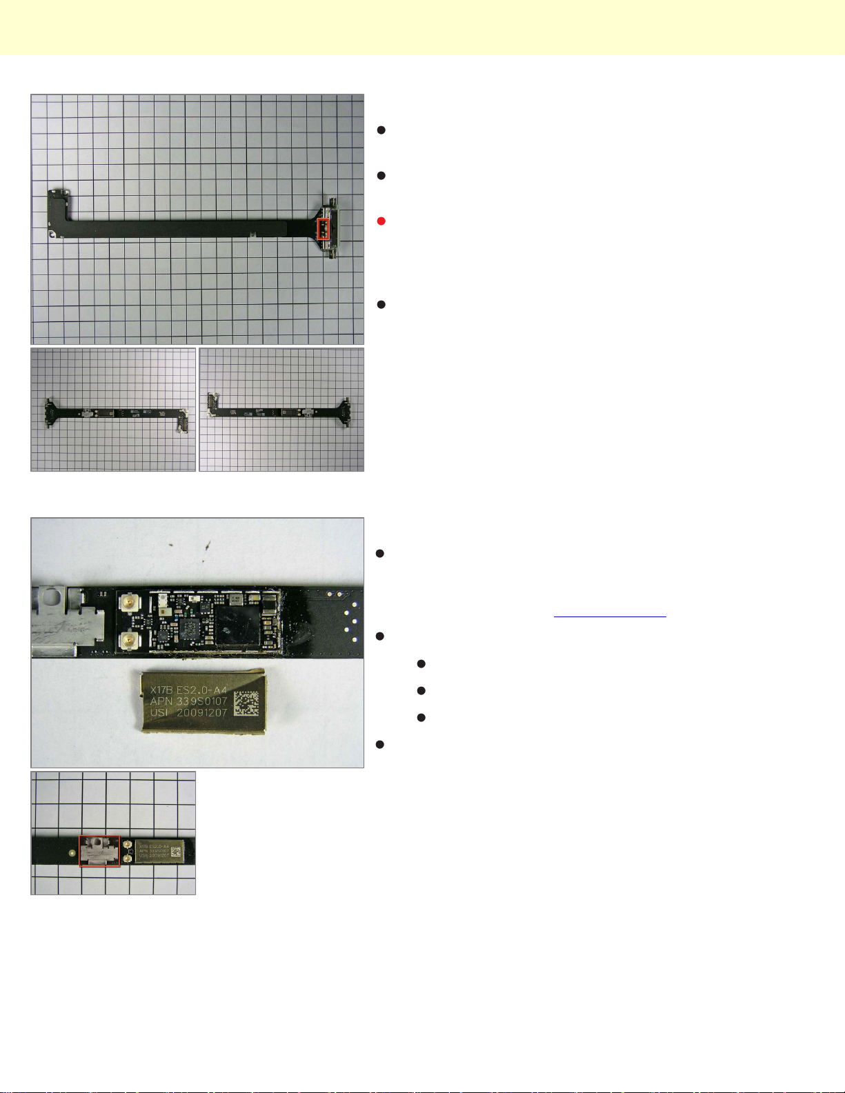
This cable carries the signal from the dock connector to
the logic board.
Never one to waste space, Apple also managed to tack
the wifi and bluetooth boards onto this cable.
Like some other Apple devices we've seen, the home
button is low-tech. There's two contact points that mate
with pads on the display assembly. When the button is
pressed, the circuit is completed.
Notably lacking from this RF/data cable is anything
GPS related.
Step 4
Wi-fi and Bluetooth are integrated into a single board.
Broadcom has been one of Apple's favorite suppliers
recently. It's possible this is the same BCM4329 chip
that Apple used in the 3rd Gen Touch.
Laser engraved on the cover:
The bracket shown in the second picture is both a cable
clip and a ground point for the WiFi/Bluetooth/cable
assembly.
X17B ES2.0-A4
APN 339S0107
USI 20091207
© 2010 iFixit — CC BY-NC-SA www.iFixit.com Page 3 of 10
Page 4
iPad FCC Teardown
Step 5
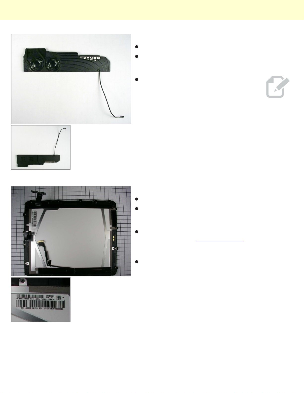
A shot of the speaker assembly.
The dual speakers provide mono sound. Two small
sealed channels direct sound toward three audio ports
carved into the bottom edge of the iPad.
The connector found on the speakers and
other components is typical of the
connectors seen in MacBook Unibody
laptops. Translation: the iPad isn't that
cramped for space.
Step 6
The inner side of the display assembly.
The part number is hard to make out, but it looks to be
LP097X02. If that's correct, then the display is made by
LG-Phillips.
This is very likely the most expensive part of the iPad. It
uses expensive IPS (in-plane switching) technology
and is LED backlit (as opposed to the cheaper TN and
CCFL backlit).
Display LED barcodes: 1579CN7346569 3225 LG0NJ
'GK65284221MTA', and 5091L-0942B 091214 R51
K319CED5D61R0094B2
© 2010 iFixit — CC BY-NC-SA www.iFixit.com Page 4 of 10
Page 5
iPad FCC Teardown
Step 7
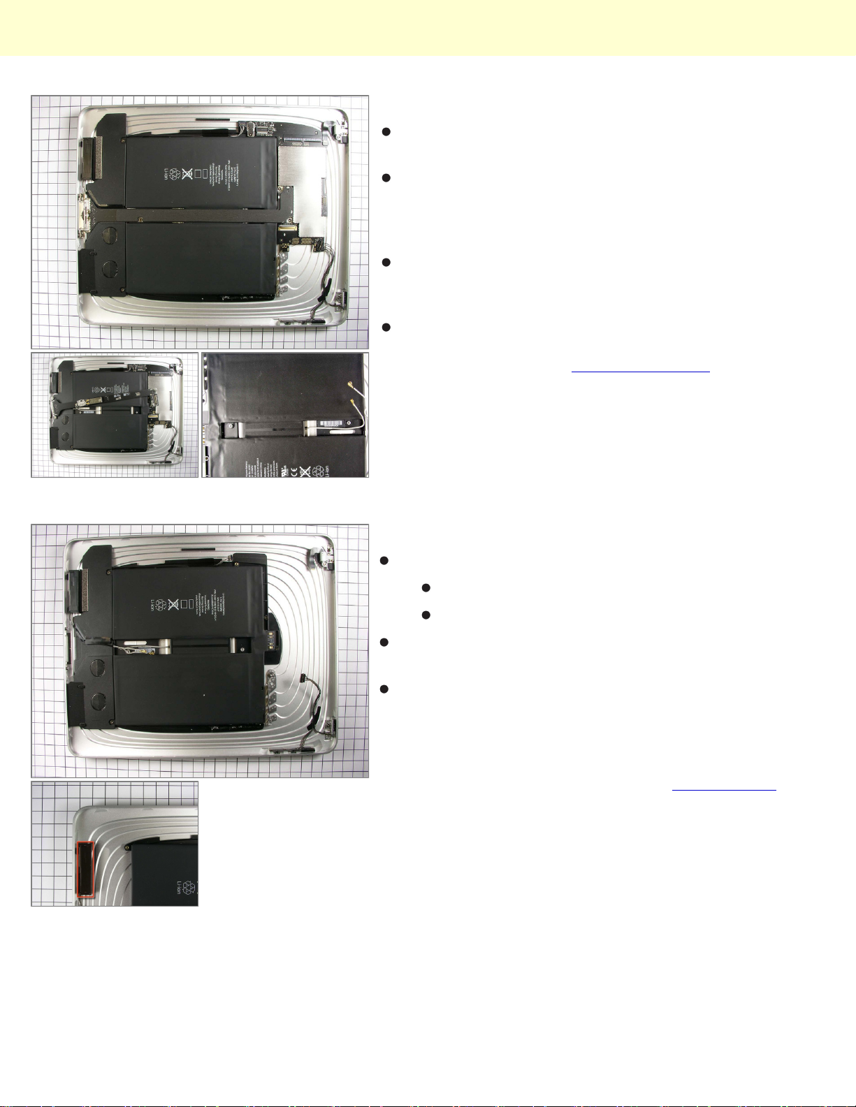
The battery is quite obvious to pick out of this picture of
the rear case (sans display assembly).
The 3.75V, 24.8 watt-hour (6.5 Amp hour [!]) battery
provides the juice for an advertised 10 hours of use. In
contrast, the iPhone 3GS has a 4.51 watt-hour battery
and the MacBook Air has a 40 watt-hour battery.
The battery seems to integrate two separate 3.75V
lithium polymer cells wired in parallel for such ample
battery life.
The USB power supply had to be enhanced specifically
for the iPad. It's a 10W unit manufactured by Foxlink
Technology, Ltd., part #A1357 W010A051.
Step 8
Some other markings on the battery:
The small black box in the second picture is one of the
WiFi antennas.
Hopefully the WiFi reception will be decent, as the back
of the iPad appears to be a single block of aluminum. In
addition to the antenna mentioned above, the Apple
logo in the center of the rear case also serves as a
window to allow for the transmission/reception of RF
signals. We saw Apple do this on the newest iMacs.
APN: 616-0447
VPN: DAK 120670-01HH00LH
© 2010 iFixit — CC BY-NC-SA www.iFixit.com Page 5 of 10
Page 6
iPad FCC Teardown
Step 9
What a lonely iPad...
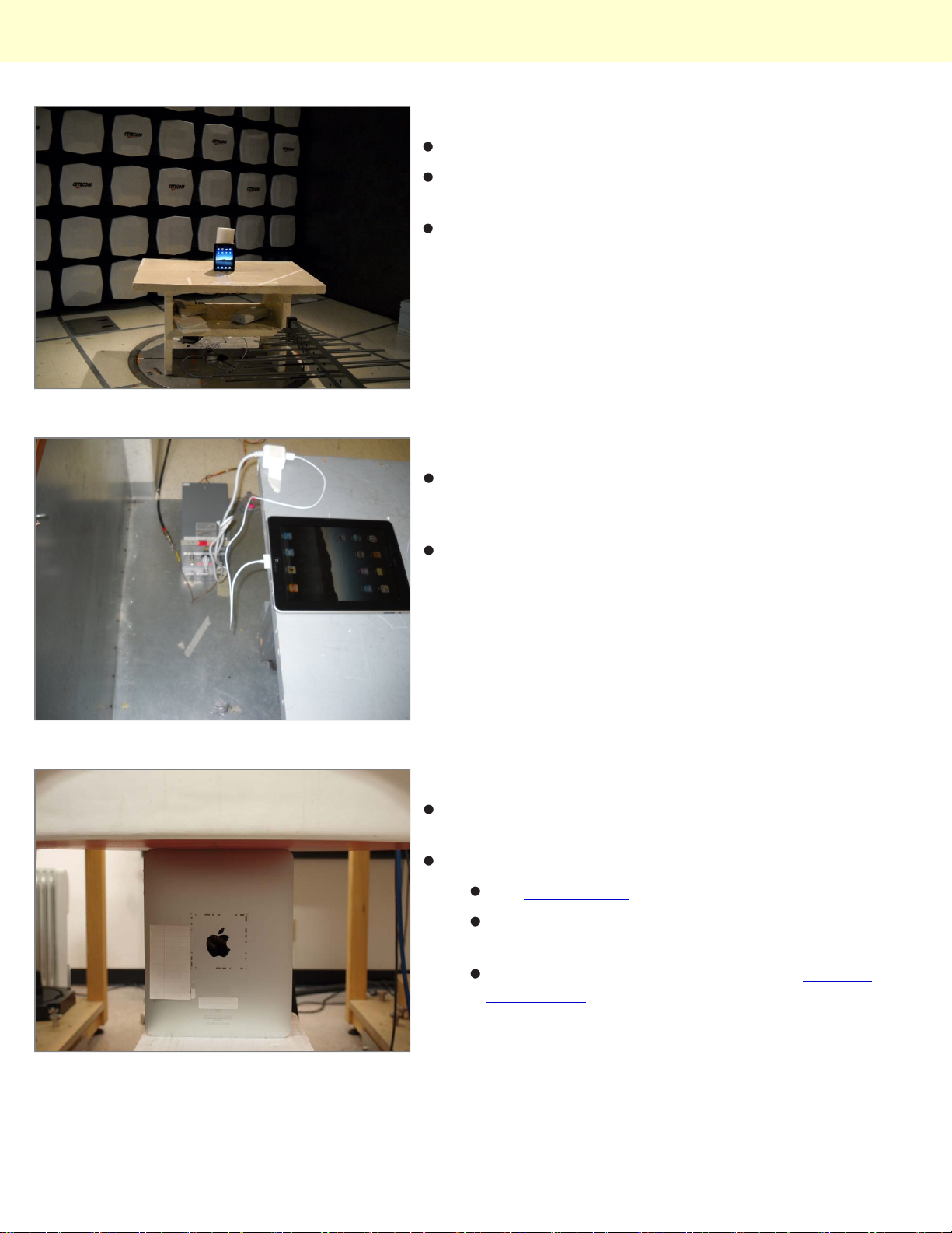
This is probably a shot inside an RF interference test
lab contracted by the FCC.
This type of test checks compliance with part 15 of the
FCC Rules and Industry Canada RSS-210: this device
must accept any interference received, including
interference that may cause undesired operation.
Step 10
This shot shows the iPad connected to what is reported
to be a LISN (Line Impedance Stabilization Network)
used for EMI testing.
This appears to be the 10W USB power adapter
available as an accessory from Apple in late April.
Step 11
This step shows the test setup used for the Specific
absorption rate report.
The FCC hosts
© 2010 iFixit — CC BY-NC-SA www.iFixit.com Page 6 of 10
The iPad manual.
The SAR evaluation report for iPad (With
802.11abgn and Bluetooth Radios).
Gratuitous amounts of test data in the FCC/IC
Test Report.
Page 7
iPad FCC Teardown
Step 12
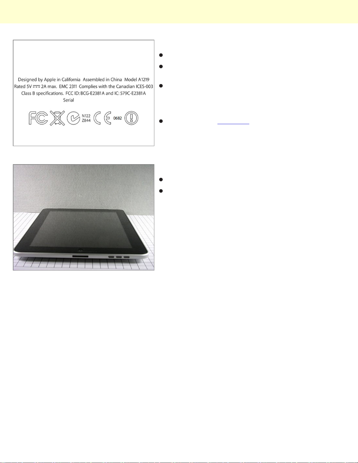
The iPad's model number of A1219 is interesting.
A1219 falls right between the 1st Gen iPod Touch
(A1213) and the MacBook Pro 15" Santa Rosa (A1226).
We would have expected the iPad to have a model
number in the A13XX range, not A12XX. It's a little
tricky to read into this, but our guess: This is indicative
of a longer than typical development cycle.
According to the FCC filing, the version that includes
3G is model A1337. Is Apple having fun with their
model numbers?
Step 13
Bottom side of iPad.
Hate how grainy/terrible these FCC pictures are? Upset
that your tax dollars are not being spent on producing
quality images of gadget guts? Tune in tomorrow as we
tear apart the iPad in 12.3 Megapixel awesomeness.
© 2010 iFixit — CC BY-NC-SA www.iFixit.com Page 7 of 10
Page 8
iPad FCC Teardown
Step 14
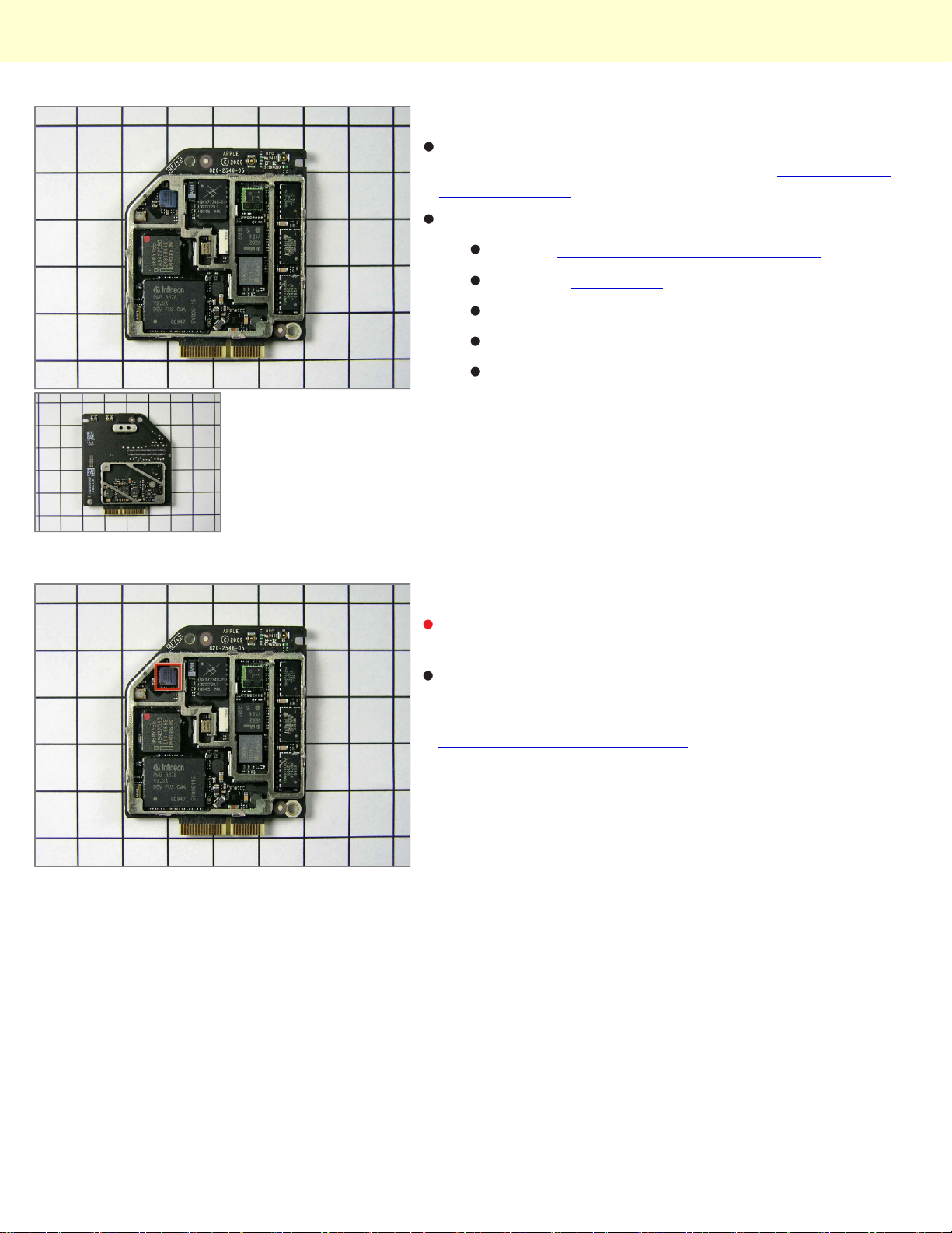
This leaked FCC photo is the communications board
from the iPad 3G. It's not linked from the primary FCC
page for the 3G.
Parts:
Infineon PMB 8878 X-Gold baseband IC.
Skyworks SKY77340 Power Amplifier Module
Three Triquint power amplifier / filters.
Infineon U6952
Numonyx 36MY1EE
Step 15
There is a Broadcom part on the top-left side, but the
FCC's photo isn't large enough to identify it.
Along the right are three TriQuint power amplifiers:
TQM616035A, TQM666032B, and TQM676031A.
These are the same three chips that Apple used in the
iPhone 3G nearly 2 years ago.
© 2010 iFixit — CC BY-NC-SA www.iFixit.com Page 8 of 10
Page 9
iPad FCC Teardown
Step 16
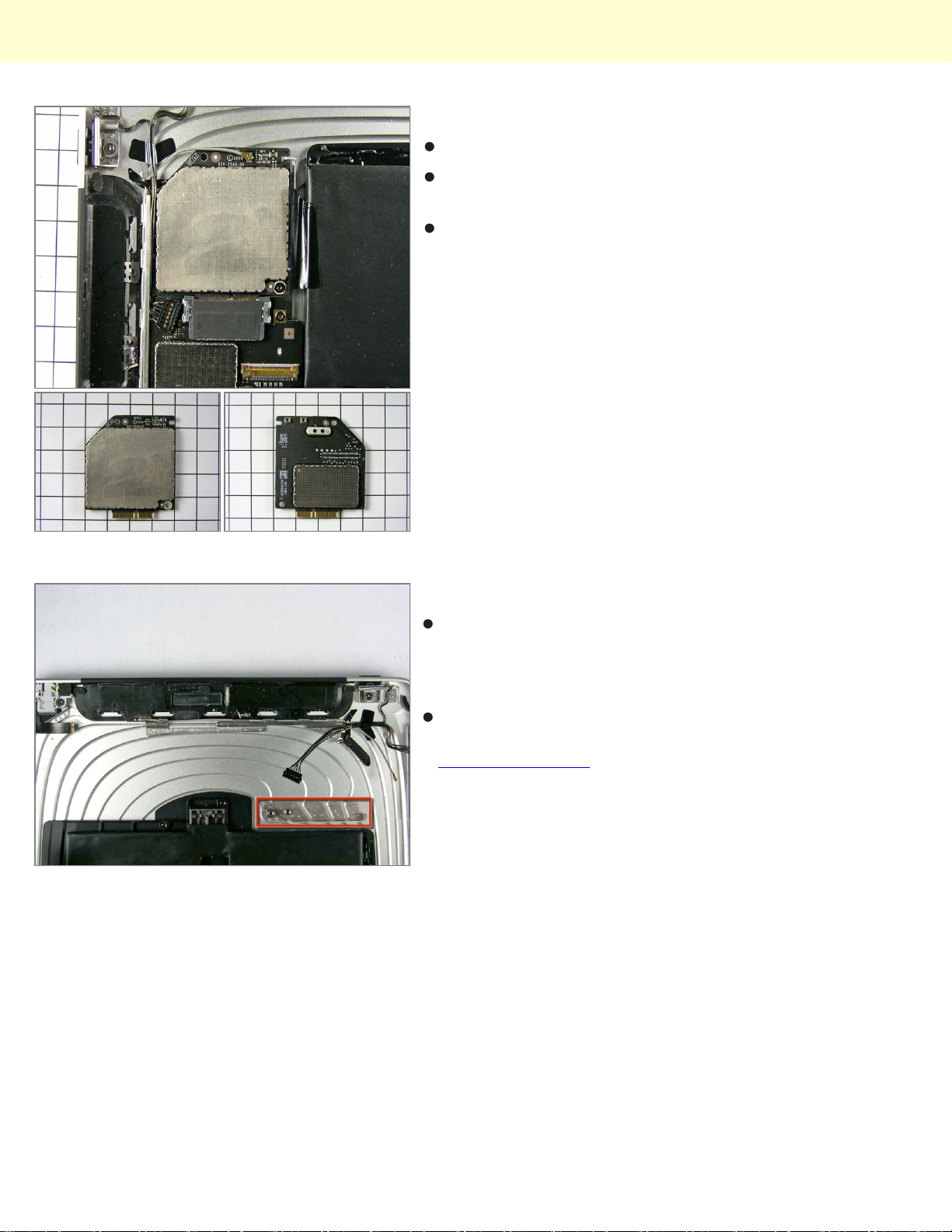
A shot of the 3G communications board.
The connector is 25 pins total; a group of 15 and a
group of 10.
Unfortunately, no, this doesn't mean you just drop this
card into your iPad to add 3G. The 3G connectivity
requires extra antennas and a modified rear casing.
Step 17
The iPad 3G has a black plastic strip along the top
edge of the rear case for transmission of signals. The
large black plastic piece at the top of this picture is the
3G antenna assembly.
The odd looking structure boxed in red is what the 3G
chip and possibly the logic board are fastened to. It is
resistance welded to the rear case and probably serves
as a ground point for the boards attached to it.
© 2010 iFixit — CC BY-NC-SA www.iFixit.com Page 9 of 10
Page 10
iPad FCC Teardown
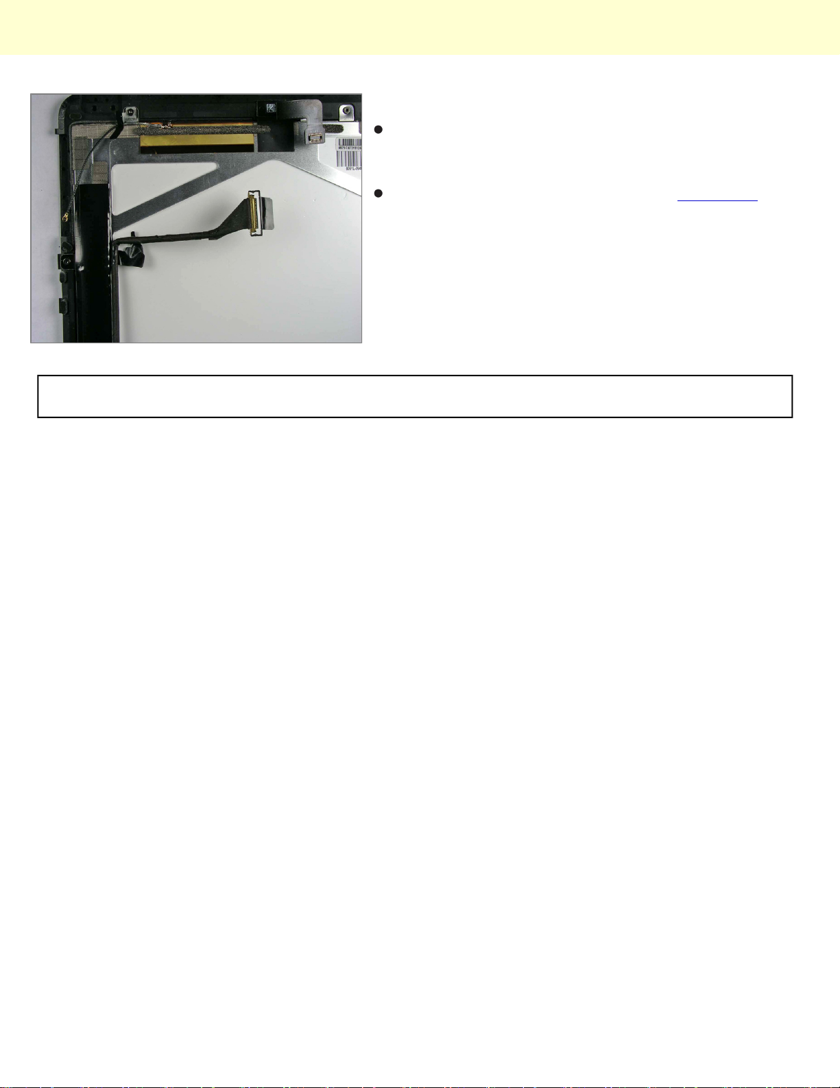
Step 18
The GPS antenna is attached to the backside of the
display assembly. It is the gold foil piece seen near the
top of the picture.
The display data cable connector is the same style
used in all of the new Unibody MacBooks.
To reassemble your device, follow these instructions in reverse order.
This document was last generated on Dec 14, 2010.
© 2010 iFixit — CC BY-NC-SA www.iFixit.com Page 10 of 10
 Loading...