

Page 1
iPad Wi-Fi Teardown
iPad Wi-Fi Teardown
Step 1 -
It's here! We got our hands on Apple's newest toy, the
iPad, and we can't wait to see what's in it. So we
won't— let's do this!
Step 2
Contents of the box:
© 2010 iFixit — CC BY-NC-SA www.iFixit.com Page 1 of 16
iPad
Dock Connector to USB Cable
10W USB Power Adapter
Documentation
Page 2
iPad Wi-Fi Teardown
Step 3
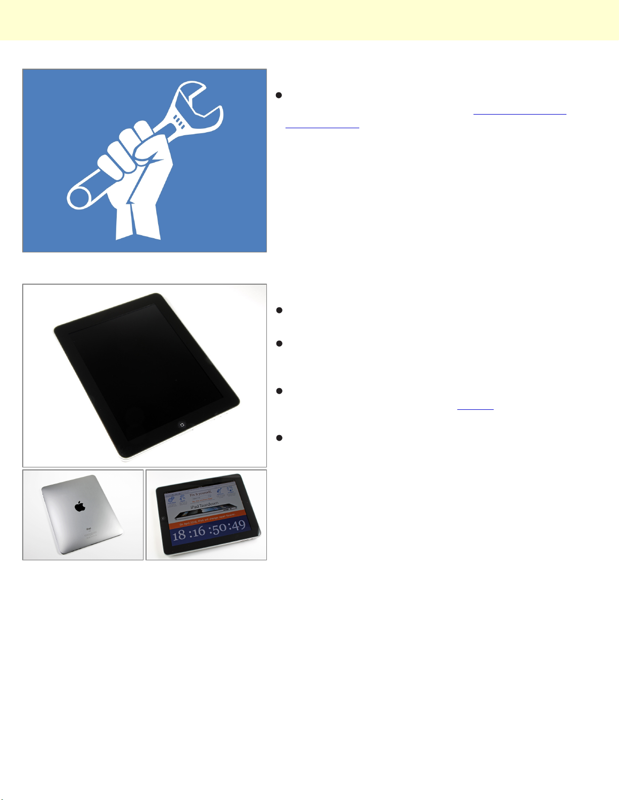
Before we proceed with our iPad teardown, a quick
announcement: On April 22, 2010, iFixit will change
repair forever.
Step 4
The iPad measures in at 242.8 x 189.7 x 13.4 mm and
weighs in at 1.5 lbs.
The significantly improved 9.7 inch LED-backlit glossy
widescreen with Multi-touch is perfect for all your movie
watching, e-book reading needs.
The iPad's model number is A1219, which doesn't
mean much. But the 3G iPad is A1337, which is rather
geeky, even for Apple.
Yes, we did turn it on—how could we not? But then we tu
rned it right back off and started figuring out how to pry
this beautiful machine apart.
© 2010 iFixit — CC BY-NC-SA www.iFixit.com Page 2 of 16
Page 3
iPad Wi-Fi Teardown
Step 5
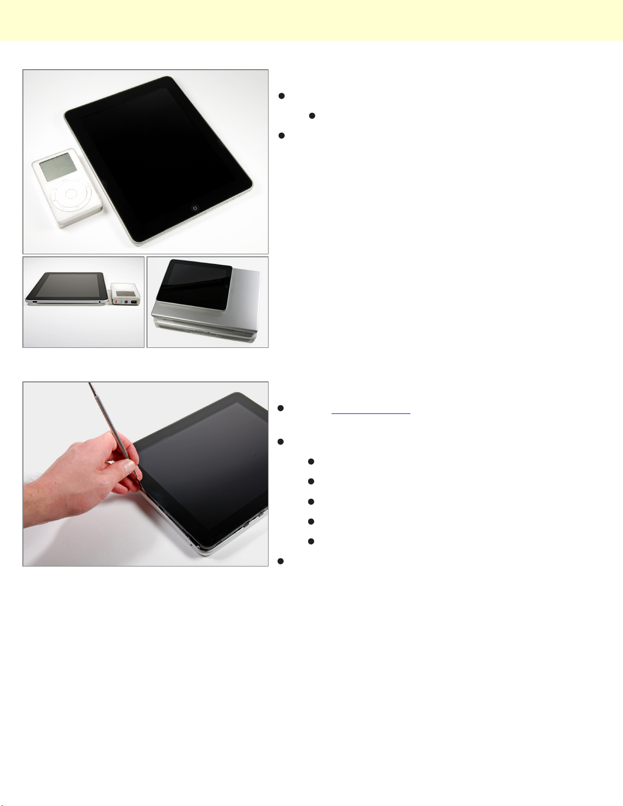
iPad, meet iPod original.
The iPad stacked upon a MacBook Pro, stacked upon a
Dell laptop.
More like: Flying saucer, meet horse & buggy.
Step 6
Insert a metal spudger between the display and the
rear case to pry the iPad open.
What an environmentally friendly device!
Environment WIN!
Arsenic-free display glass
BFR-free
Mercury-free LCD display
PVC-free
Recyclable aluminum and glass enclosure
© 2010 iFixit — CC BY-NC-SA www.iFixit.com Page 3 of 16
Page 4
iPad Wi-Fi Teardown
Step 7
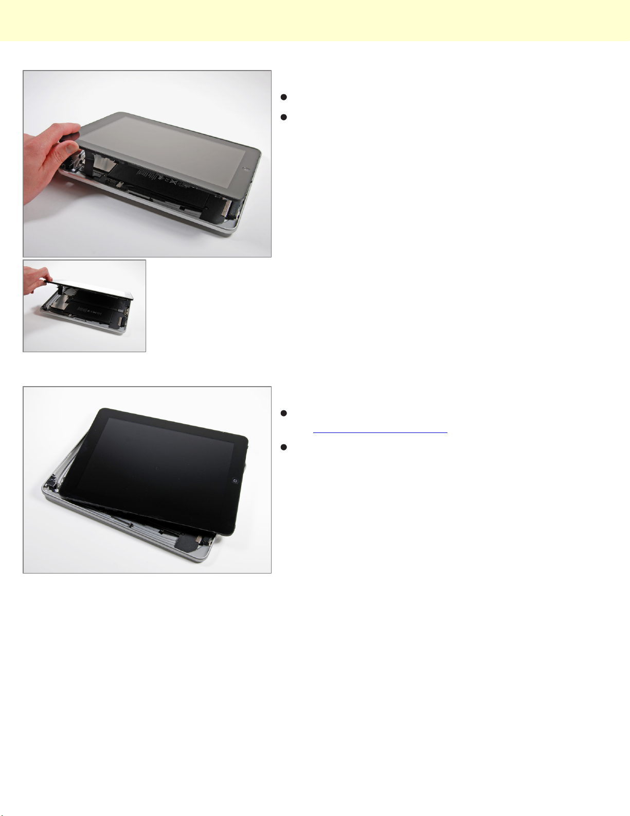
Lift the display assembly away from the rear case.
A first peek under the hood reveals two huge Li-ion
Polymer batteries taking up most of the space in this
device.
Step 8
Aaaand it's off. You have no idea how glad we are that
this didn't require a heat gun.
Words from the wise: You might break some tabs
getting the display assembly off.
© 2010 iFixit — CC BY-NC-SA www.iFixit.com Page 4 of 16
Page 5
iPad Wi-Fi Teardown
Step 9
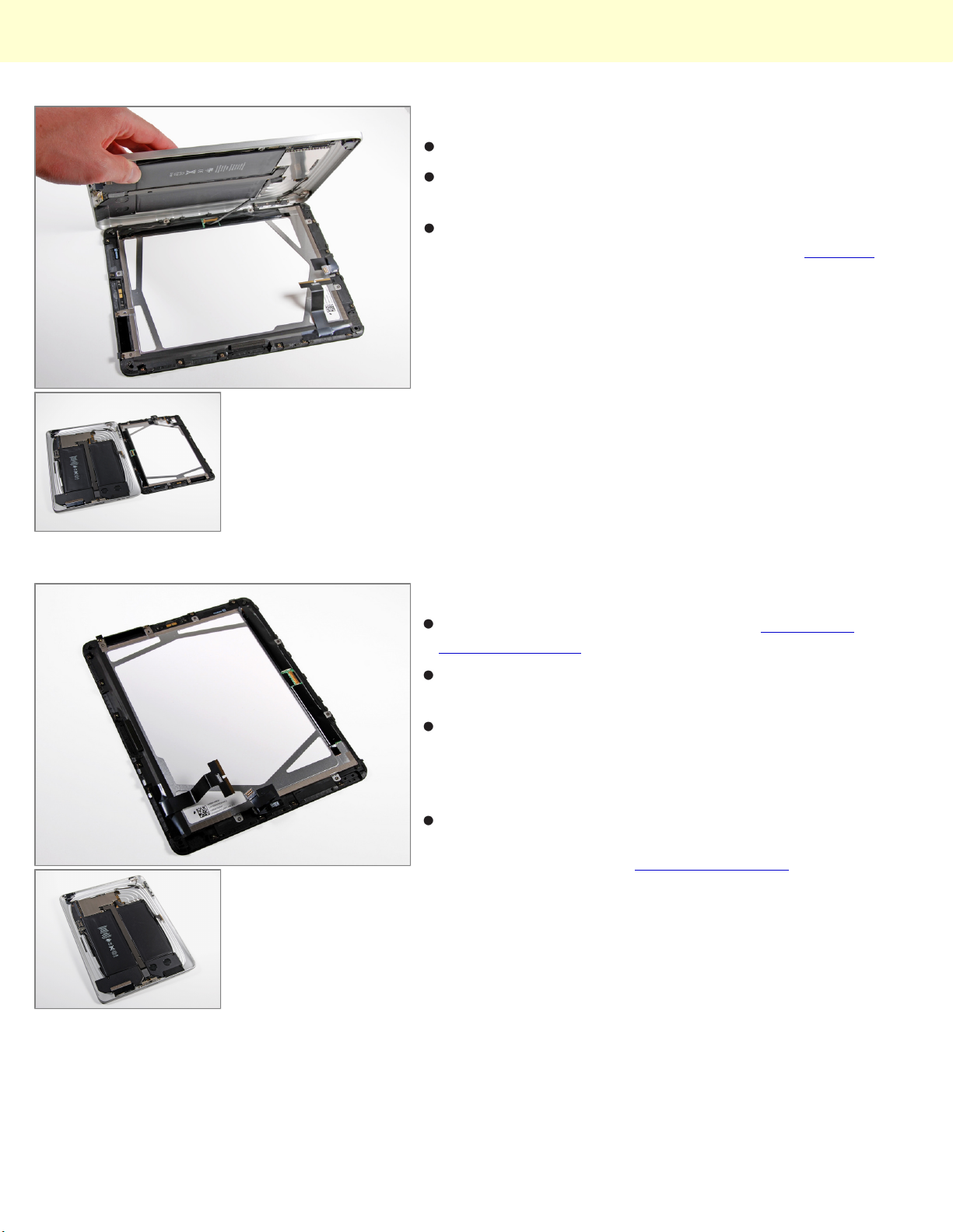
Wow, what gorgeous symmetry.
The display assembly and rear case assembly are each
350g. Talk about 50/50 weight distribution.
The empty void in the upper right corner is where the
cellular communications board will go in the 3G iPad.
Step 10
The display has a marking referencing Honeywell
patent #5280371.
It looks pretty barren, mostly because all the 3G
equipment is missing.
The 3.75V, 24.8 watt-hour battery provides the juice for
an advertised 10 hours of use. In contrast, the iPhone
3GS has a 4.51 watt-hour battery and the MacBook Air
has a 40 watt-hour battery.
The USB power supply had to be enhanced specifically
for the iPad. It's a 10W unit manufactured by Foxlink
Technology, Ltd., part #A1357 W010A051.
© 2010 iFixit — CC BY-NC-SA www.iFixit.com Page 5 of 16
Page 6
iPad Wi-Fi Teardown
Step 11
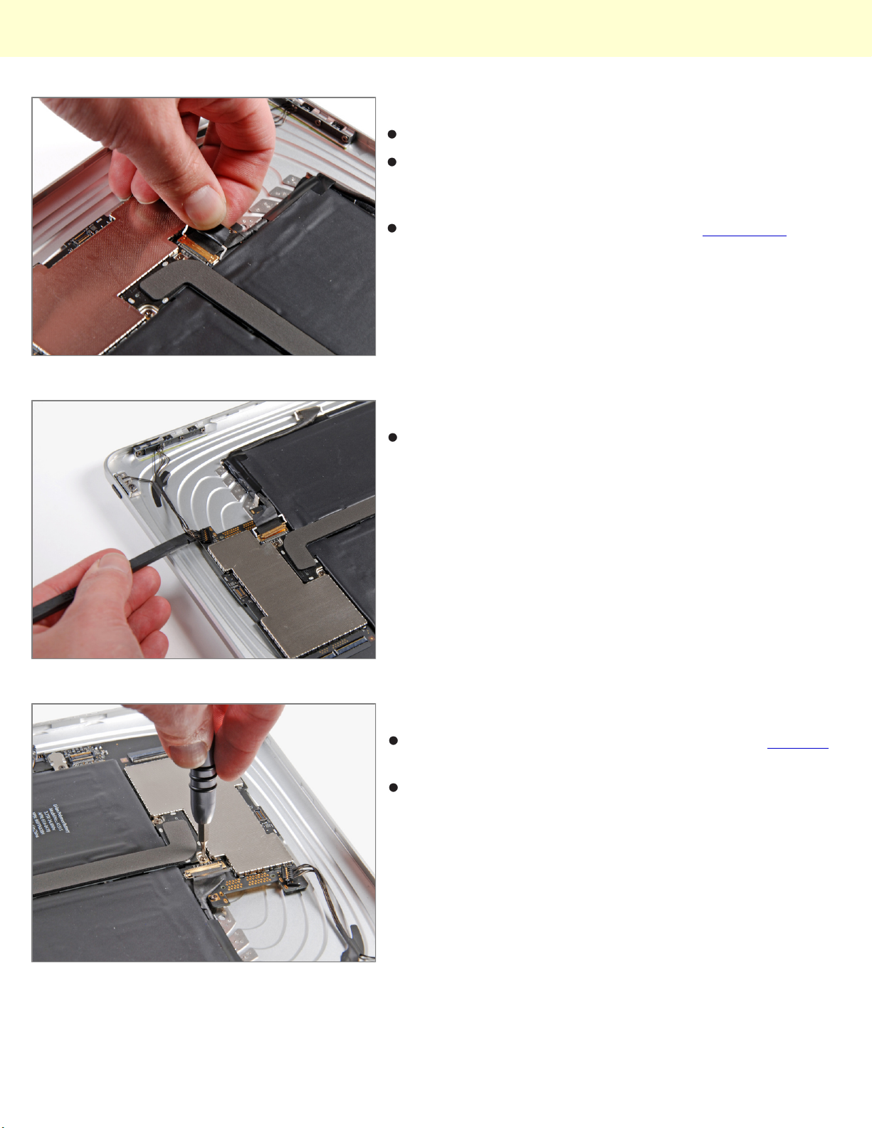
Disconnecting the display data cable.
Removing these connectors is a two step process. You
first have the flip up the locking bar (pictured) and can
then slide the cable out of the socket.
The display data cable connector is the same style
used in all of the new Unibody MacBooks.
Step 12
Disconnecting the volume, power, and screen rotation
lock buttons connector.
Step 13
The main board is secured to the back panel by T4 Torx
screws.
We have never seen Apple use screws with a bit this
small before.
© 2010 iFixit — CC BY-NC-SA www.iFixit.com Page 6 of 16
Page 7
iPad Wi-Fi Teardown
Step 14
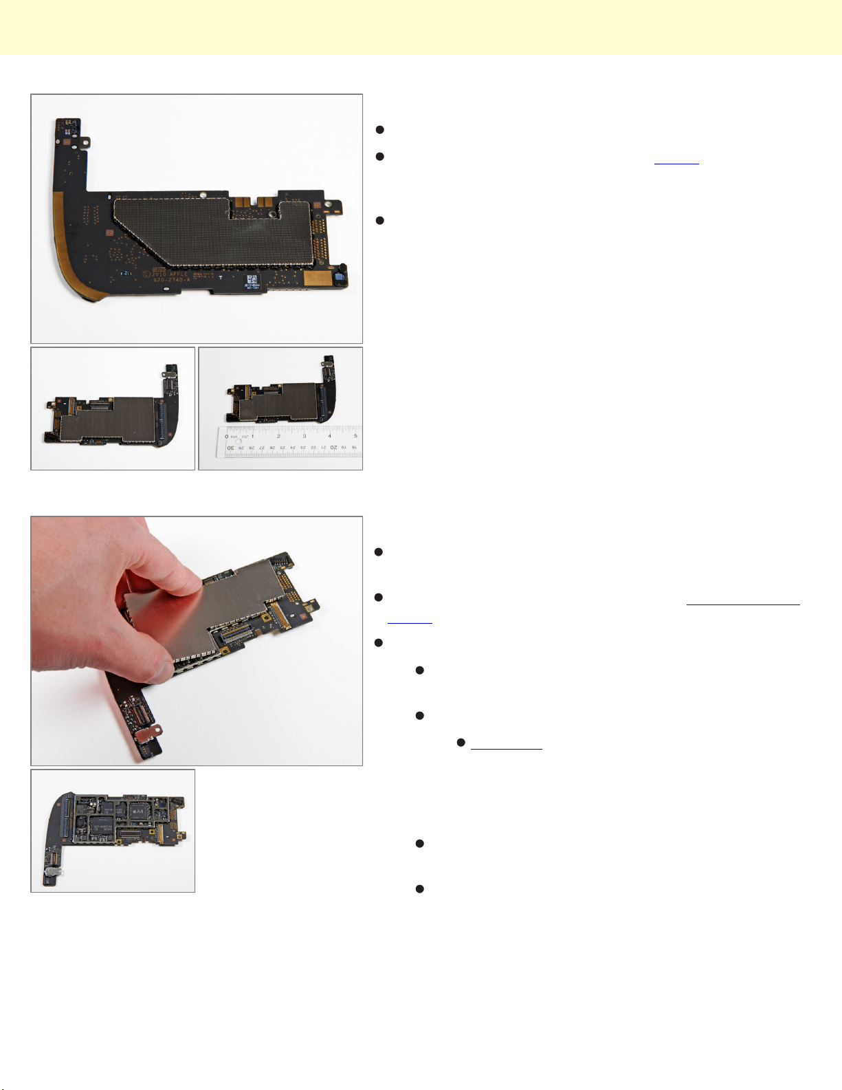
Top and bottom of logic board with the EMI shield on.
It looks like this board was made by AT&S. We haven't
seen Apple's PCB manufacturers brand their boards
before.
The logic board is about 4.5" wide, spanning about 60%
of the iPad's width.
Step 15
Remove the EMI shield from the logic board, and
presto!
This board is markedly different than the pre-production
board we uncovered.
Markings on the A4:
N26CGM0T 1007 APL0398 33950084 YNL184A2
1004 K4X2G643GE
Yes, the K4X2 is a Samsung DRAM part number!
Decoding the part number shows there is
2Gb of memory inside. This translates into
~128MB of memory per die, for 256 MB
total. (NOT 512MB, as we previously
reported.)
This means the A4 processor is probably being
manufactured by Samsung.
The DRAM was stamped at the end of January,
while the processor die was likely manufactured
the third week of February.
© 2010 iFixit — CC BY-NC-SA www.iFixit.com Page 7 of 16
Page 8
iPad Wi-Fi Teardown
Step 16
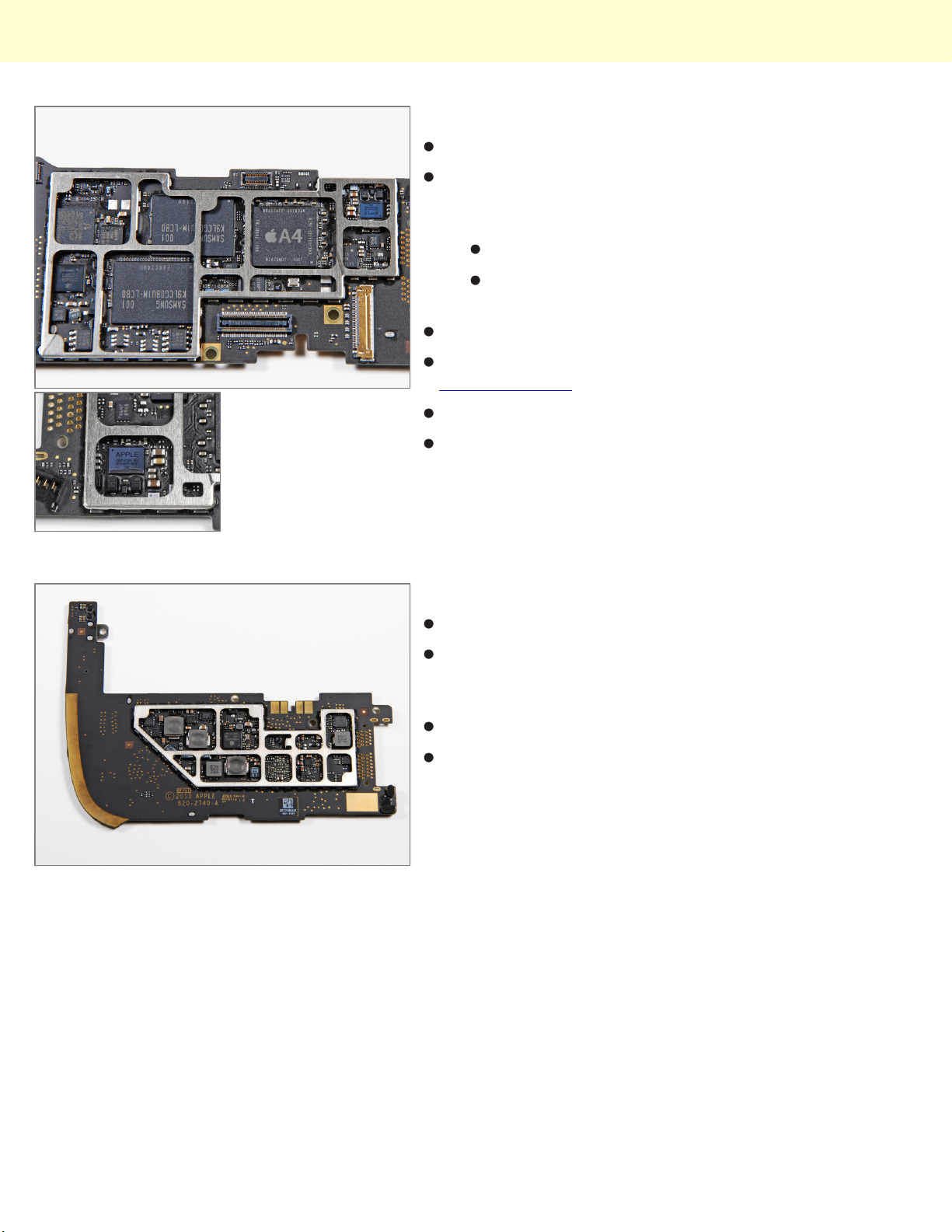
A shot of the logic board minus the steel EMI shield.
The manufacturer of the memory has switched from
Toshiba on the FCC teardown to Samsung on this
device.
Broadcom BCM5973 I/O controller.
The Apple A4 is marked up much nicer than the part in
the FCC photos from yesterday.
Texas Instruments CD3240A1
NXP: L061 01 4 ZSD950
64Gbit MLC NAND flash.
We love how much easier Samsung's chip
numbers are to interpret.
Step 17
A reverse shot of the logic board.
The gold strip on the curved edge most likely helps
ground the board against the "steps" cut into the
aluminum rear case.
Apple part #820-2740-A.
The Apple-branded IC on this side of the board is
labeled 338S0805.
© 2010 iFixit — CC BY-NC-SA www.iFixit.com Page 8 of 16
Page 9
iPad Wi-Fi Teardown
Step 18
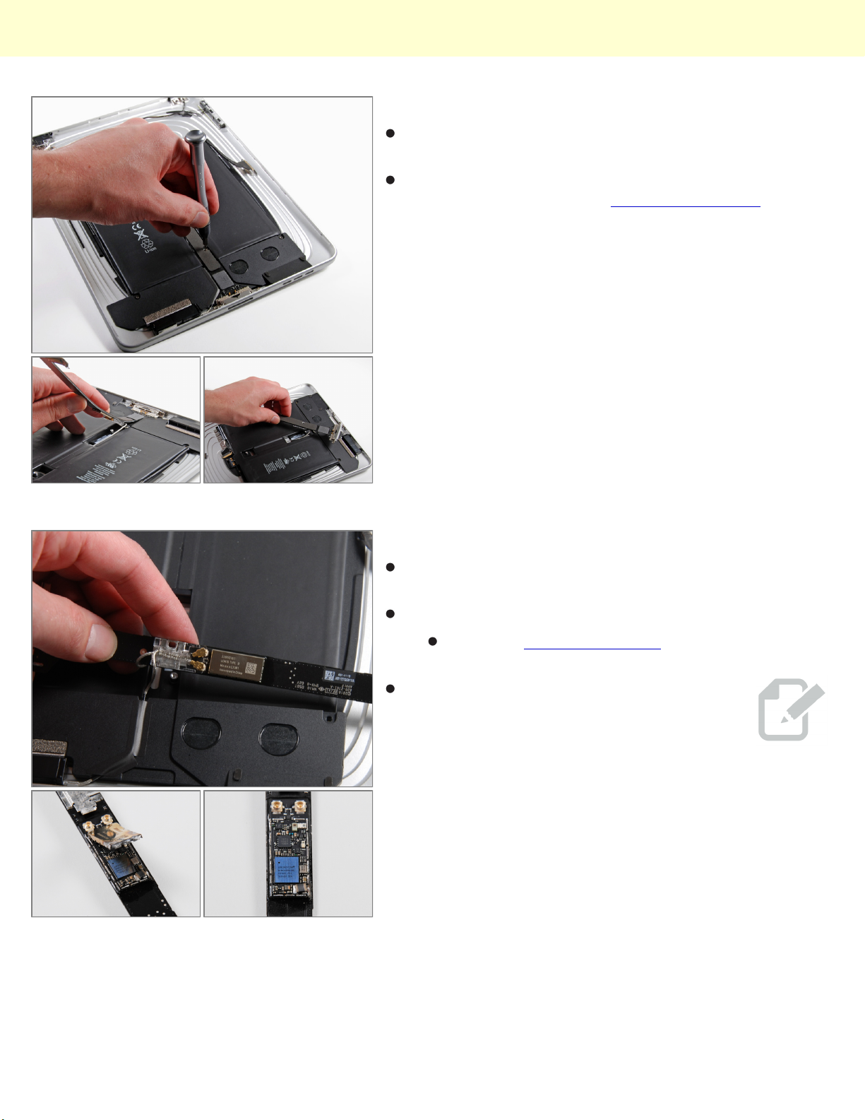
Removing the single screw securing the dock
connector cable to the rear case.
Notably lacking from this RF/data cable is anything
GPS related. Check out the FCC iPad teardown to see
where the GPS will be in the 3G device.
Step 19
The 802.11n WiFi/Bluetooth card is integrated into the
dock connector cable.
Hiding under the case:
Dont worry, the capacitor near the lower
right corner of the Broadcom chip didn't
come that way. The solder melted and it
moved when we heated the steel casing to
remove it.
Broadcom BCM4329XKUBG 802.11n WiFi +
Bluetooth 2.1 + EDR and FM
© 2010 iFixit — CC BY-NC-SA www.iFixit.com Page 9 of 16
Page 10
iPad Wi-Fi Teardown
Step 20
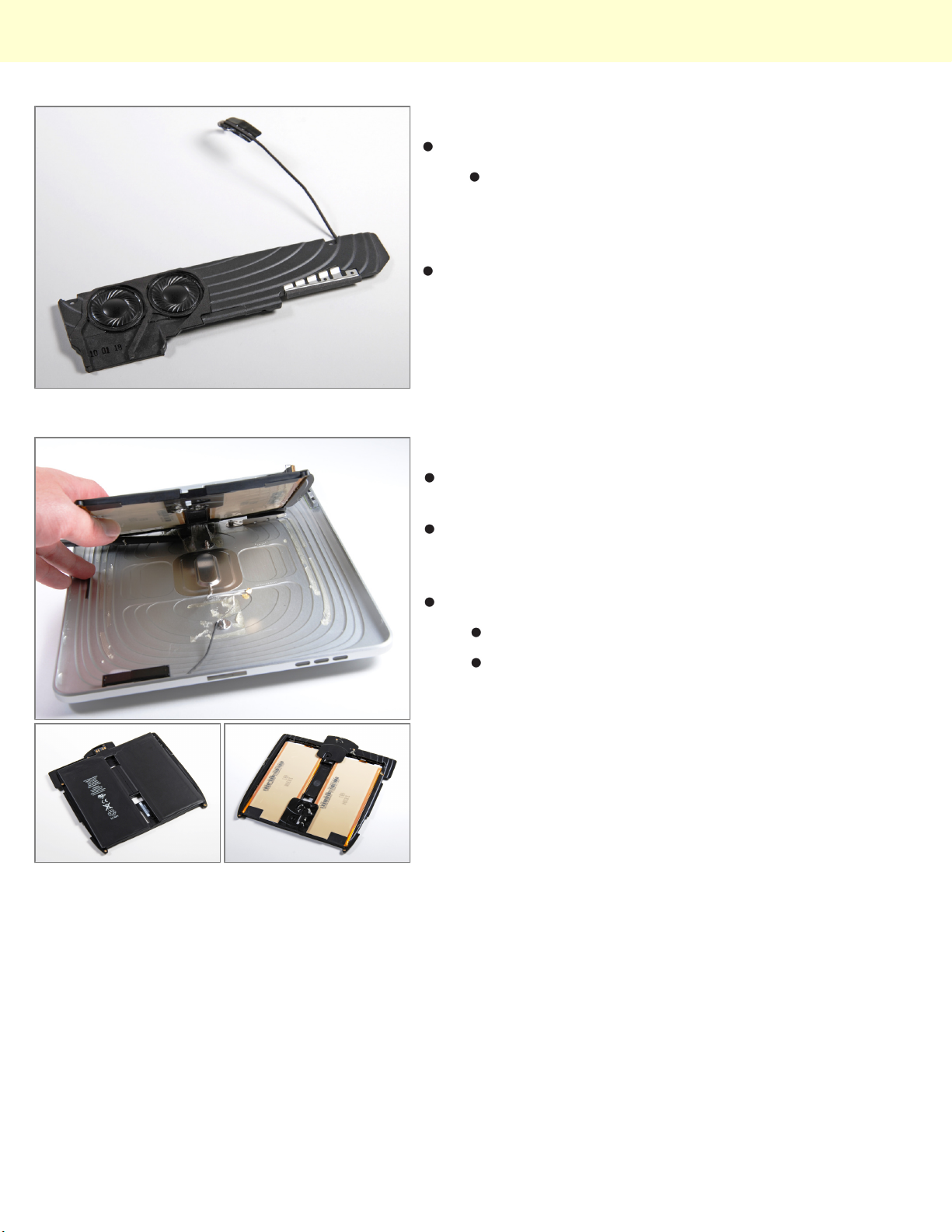
The speaker assembly is larger than we expected:
Dual speakers provide mono sound. Two small sealed
channels direct sound toward three audio ports carved
into the bottom edge of the iPad. The audio-out jack
provides stereo sound, of course.
Step 21
That's a hulk of a battery: it weighs 148g with the
casing.
Confirming our suspicions from yesterday, the battery
integrates two separate 3.75V lithium polymer cells
wired in parallel for such ample battery life.
The connector found on the speakers and other
components is typical of the connectors seen in
MacBook Unibody laptops. Translation: the iPad
isn't that cramped for space.
Battery cell markings:
P11GA6-01-C01F
741-00310A +
© 2010 iFixit — CC BY-NC-SA www.iFixit.com Page 10 of 16
Page 11
iPad Wi-Fi Teardown
Step 22
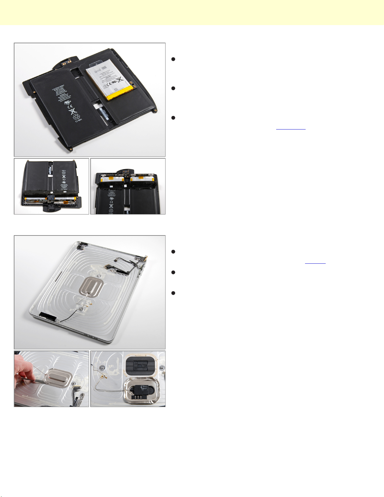
The iPad battery is a lot bigger than an iPhone 3G
battery. The iPhone battery has about 1/5th the
capacity provided by the iPad battery.
The second shot shows the battery cover peeled back
to expose the protection and connection circuitry for
each Li-Poly battery.
The third shot shows the other side of the battery
board, which is stamped with Compeq.
Step 23
The bare rear case. The antenna behind the apple logo
looks just like the antenna on the new iMacs.
A little prying with a metal spudger is required to
separate the antenna from the rear case.
Tolerances look pretty tight in the antenna
compartment. Check out that pocket just for the
antenna to sit in.
© 2010 iFixit — CC BY-NC-SA www.iFixit.com Page 11 of 16
Page 12
iPad Wi-Fi Teardown
Step 24
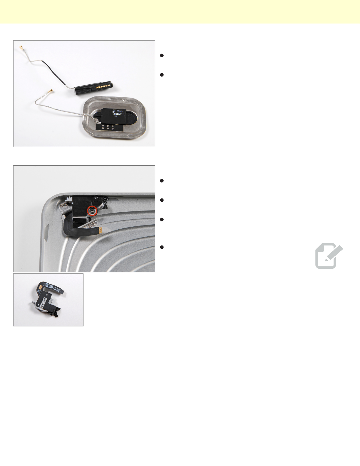
Here's a detail shot of both WiFi antennas. The wireless
reception should be decent with such dense antennas.
Adding 3G capability to a Wi-Fi only iPad is not going to
be a very feasible upgrade. Based on the photos
released by the FCC, the 3G models include additional
antennas as well as a plastic strip in the rear panel to
improve reception.
Step 25
Remove a couple screws and pull the headphone jack
out of the rear case.
As with most portable devices, the headphone jack is
very well fastened to the case.
The microphone's right next to the headphone jack and
goes through the same data cable as the headphone
jack.
Like the iPhone, it appears that the iPad
features a liquid sensor in its headphone
jack. If you get your iPad wet, don't expect
Apple to fix it under warranty for you.
© 2010 iFixit — CC BY-NC-SA www.iFixit.com Page 12 of 16
Page 13
iPad Wi-Fi Teardown
Step 26
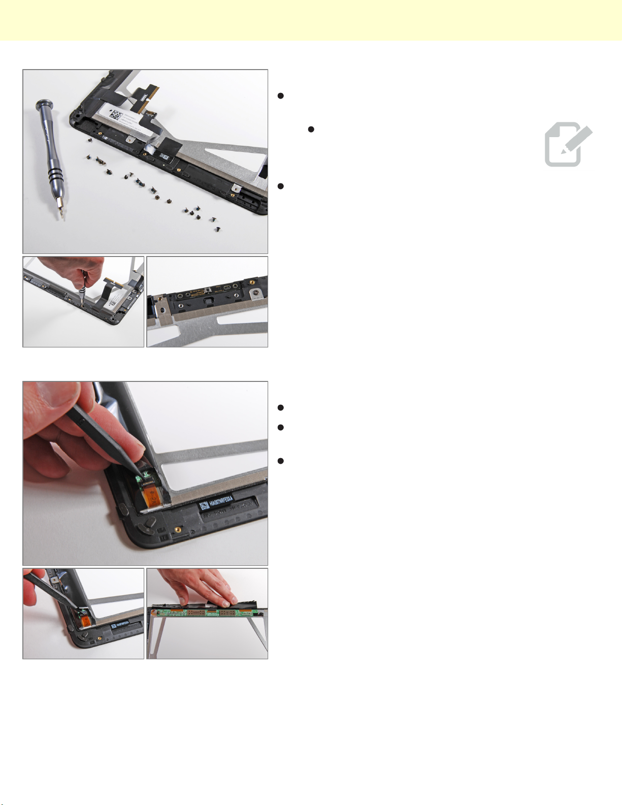
Ants on parade? Nope, just the T4 Torx screws holding
each tab to the display assembly.
Luckily, the home button is a digital switch with its own
circuit board, making replacement that much easier.
Each clip holding the display assembly
to the rear case is fastened down with
its own T4 Torx screw.
Step 27
Disassembling the display assembly.
A thin ribbon cable connects the LED driver board to
the LED backlights.
The LED driver circuitry and the interconnects between
the actual LCD and the display data cable connector
are contained within the same circuit board.
© 2010 iFixit — CC BY-NC-SA www.iFixit.com Page 13 of 16
Page 14
iPad Wi-Fi Teardown
Step 28
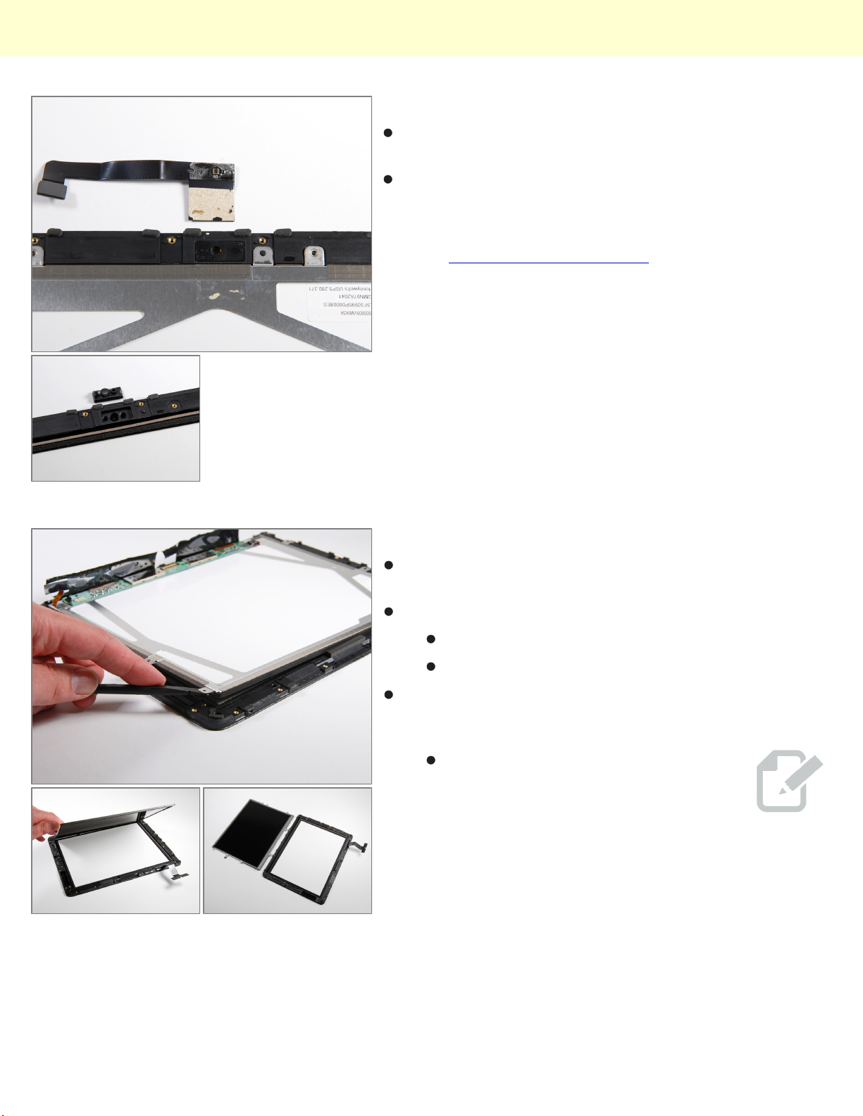
The ambient light sensor lives in a compartment that a
camera would love to call home.
We suspect that this compartment was intended for the
ambient light sensor all along, and the rumors of a
camera that would fit here were overzealous. The
layout does look very similar to the camera's view ports
on the MacBook Pro 13" Unibody.
Step 29
The display seems to be glued around its perimeter but
can still be removed from the plastic framework.
The display assembly weighs in at:
The glass seems quite thick (~1.18 mm), which is not a
huge surprise considering the size of the iPad.
Compare that to about 1.02 mm for the iPhone.
153g for the LCD
193g for the front glass
The iPad would require thicker glass
due to the increased "lever arm"
caused by pressing down at the center
of the screen. This is analogous to the
difficulty of bending a one inch section
of a ruler compared to bending the
entire twelve inch ruler.
© 2010 iFixit — CC BY-NC-SA www.iFixit.com Page 14 of 16
Page 15
iPad Wi-Fi Teardown
Step 30
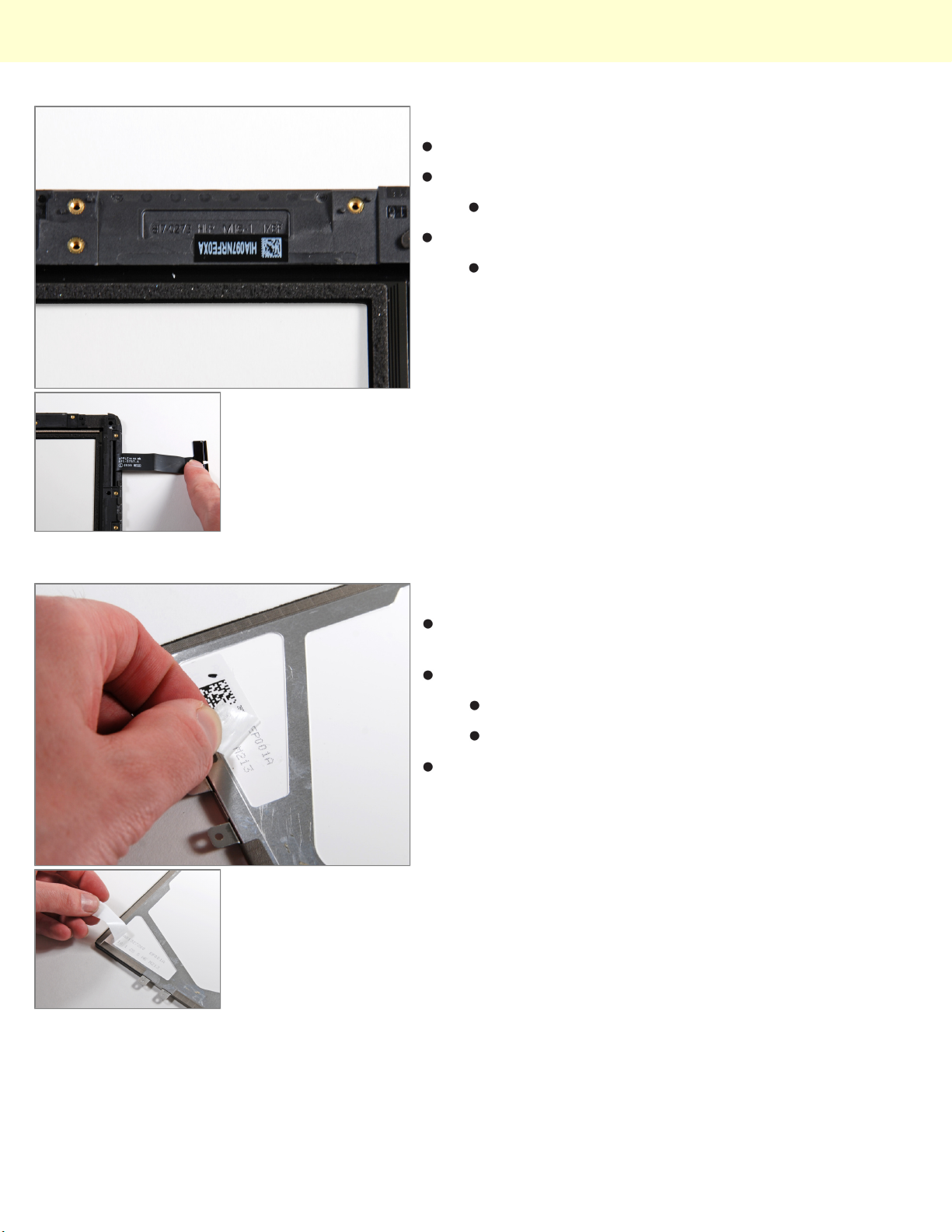
Some front glass/digitizer part numbers.
The part number on the display frame reads:
On the digitizer cable:
HIA097NRFE0XA
821-0757-A
Step 31
Peel back the sticker, and more part numbers can be
seen near the bottom of the LCD.
The numbers read:
We don't know who made this particular LCD. Do you?
Another iPad we opened contained a LCD panel that
was manufactured by LG.
A01327200 EP001A
10 1 25 S NE M213
© 2010 iFixit — CC BY-NC-SA www.iFixit.com Page 15 of 16
Page 16
iPad Wi-Fi Teardown
Step 32
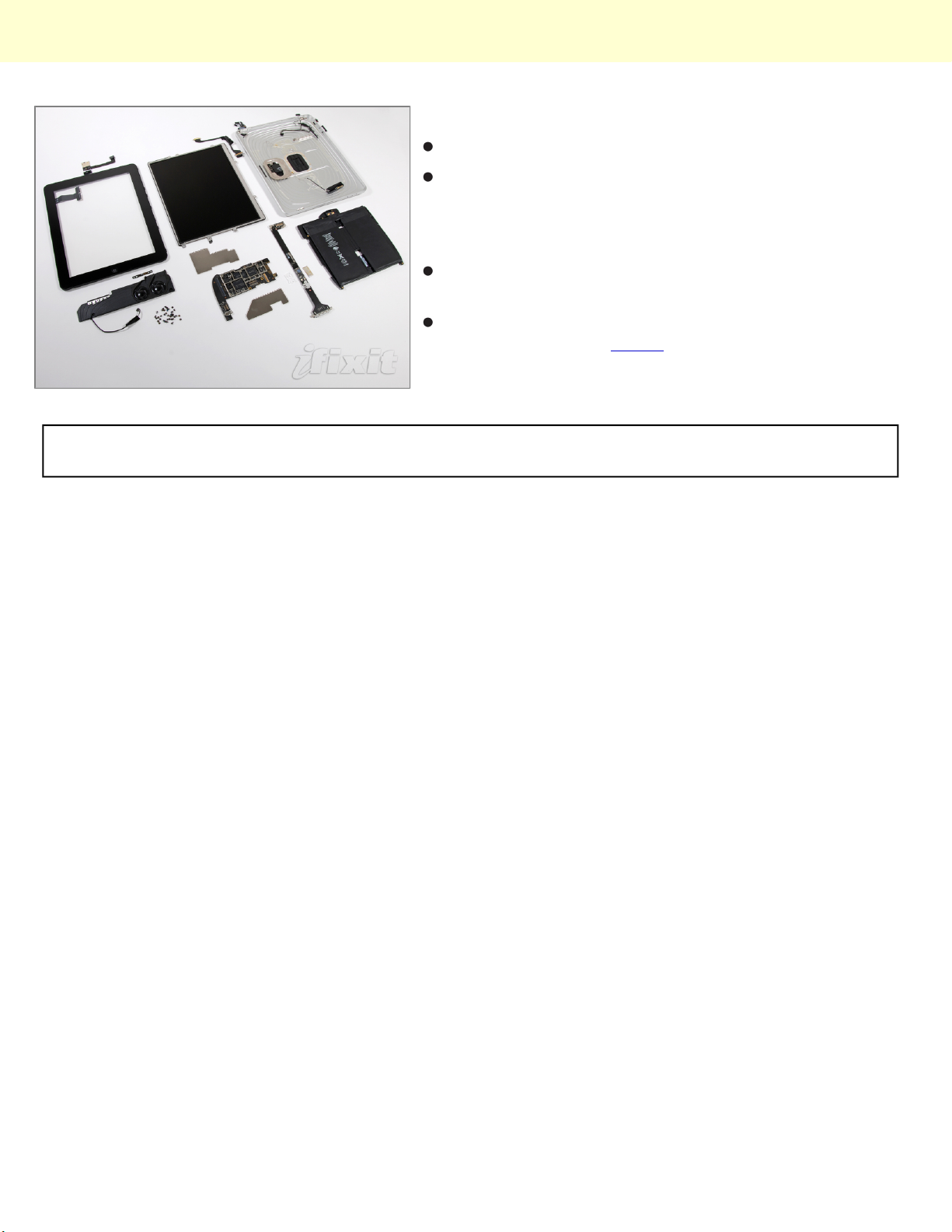
As always, the final layout shot.
Here's the weight breakdown: Aluminum back: 138
grams, Battery: 148 grams, LCD: 153 grams, Glass
(and frame): 193 grams, Speaker: 17 grams, Main
board: 21 grams, Everything else: 27 grams
Total: 697 grams (that's more than the .68 kg Apple
quotes, has anyone else weighed their complete iPad?)
This iPad may be apart, but we'll continue to dig deeper
into its chips. Follow @ifixit for the latest updates!
To reassemble your device, follow these instructions in reverse order.
© 2010 iFixit — CC BY-NC-SA www.iFixit.com Page 16 of 16
 Loading...