Apex PA12, PA12A Datasheet

MICROTECHNOLOGY
HTTP://WWW.APEXMICROTECH.COM (800) 546-APEX (800) 546-2739
FEATURES
• LOW THERMAL RESISTANCE — 1.4°C/W
• CURRENT FOLDOVER PROTECTION — NEW
• HIGH TEMPERATURE VERSION — PA12H
• EXCELLENT LINEARITY — Class A/B Output
• WIDE SUPPLY RANGE — ±10V to ±50V
• HIGH OUTPUT CURRENT — Up to ±15A Peak
APPLICATIONS
POWER OPERATIONAL AMPLIFIERS
PA12 • PA12A
• MOTOR, VALVE AND ACTUATOR CONTROL
• MAGNETIC DEFLECTION CIRCUITS UP TO 10A
• POWER TRANSDUCERS UP TO 100kHz
• TEMPERATURE CONTROL UP TO 360W
• PROGRAMMABLE POWER SUPPLIES UP TO 90V
• AUDIO AMPLIFIERS UP TO 120W RMS
DESCRIPTION
The PA12 is a state of the art high voltage, very high output
current operational amplifier designed to drive resistive, inductive and capacitive loads. For optimum linearity, especially at
low levels, the output stage is biased for class A/B operation
using a thermistor compensated base-emitter voltage multiplier circuit. The safe operating area (SOA) can be observed
for all operating conditions by selection of user programmable current limiting resistors. For continuous operation
under load, a heatsink of proper rating is recommended.
This hybrid integrated circuit utilizes thick film (cermet)
resistors, ceramic capacitors and semiconductor chips to
maximize reliability, minimize size and give top performance.
Ultrasonically bonded aluminum wires provide reliable interconnections at all operating temperatures. The 8-pin TO-3
package is hermetically sealed and electrically isolated. The
use of compressible isolation washers voids the warranty.
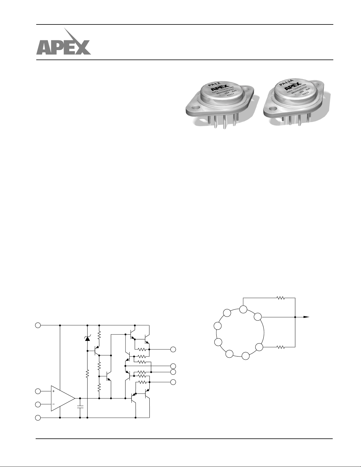
EQUIVALENT SCHEMATIC
3
Q3
Q5
Q2A
Q6A
Q2B
Q6B
D1
Q1
Q4
4
A1
5
C1
6
POWER RATING
Not all vendors use the same method to rate the power
handling capability of a Power Op Amp. APEX rates the
internal dissipation, which is consistent with rating methods
used by transistor manufacturers and gives conservative
results. Rating delivered power is highly application dependent and therefore can be misleading. For example, the 125W
internal dissipation rating of the PA12 could be expressed as
an output rating of 250W for audio (sine wave) or as 440W if
using a single ended DC load. Please note that all vendors rate
maximum power using an infinite heatsink.
THERMAL STABILITY
APEX has eliminated the tendency of class A/B output
stages toward thermal runaway and thus has vastly increased
amplifier reliability. This feature, not found in most other Power
Op Amps, was pioneered by APEX in 1981 using thermistors
which assure a negative temperature coefficient in the quiescent current. The reliability benefits of this added circuitry far
outweigh the slight increase in component count.
EXTERNAL CONNECTIONS
R
CL+
TOP VIEW
6
2
7
F.O.
CL+
1
8
CL–
OUT
OUTPUT
R
CL–
+V
S
3
+IN
4
–IN
5
2
–V
S
1
7
8
APEX MICROTECHNOLOGY CORPORATION • TELEPHONE (520) 690-8600 • FAX (520) 888-3329 • ORDERS (520) 690-8601 • EMAIL prodlit@apexmicrotech.com

PA12 • PA12A
ABSOLUTE MAXIMUM RATINGS
SPECIFICATIONS
ABSOLUTE MAXIMUM RATINGS
SPECIFICATIONS
PARAMETER TEST CONDITIONS
INPUT
OFFSET VOLTAGE, initial TC = 25°C ±2 ±6 ±1 ±3mV
OFFSET VOLTAGE, vs. temperature Full temperature range ±10 ±65 * ±40 µV/°C
OFFSET VOLTAGE, vs. supply TC = 25°C ±30 ±200 * * µV/V
OFFSET VOLTAGE, vs. power TC = 25°C ±20 * µV/W
BIAS CURRENT, initial TC = 25°C ±12 ±30 10 20 nA
BIAS CURRENT, vs. temperature Full temperature range ±50 ±500 * * pA/°C
BIAS CURRENT, vs. supply TC = 25°C ±10 * pA/V
OFFSET CURRENT, initial TC = 25°C ±12 ±30 ±5 ±10 nA
OFFSET CURRENT, vs. temperature Full temperature range ±50 * pA/°C
INPUT IMPEDANCE, DC TC = 25°C200*MΩ
INPUT CAPACITANCE TC = 25°C3*pF
COMMON MODE VOLTAGE RANGE3Full temperature range ±VS –5 ±VS –3 * * V
COMMON MODE REJECTION, DC Full temp. range, VCM = ±VS –6V 74 100 * * dB
GAIN
OPEN LOOP GAIN at 10Hz TC = 25°C, 1KΩ load 110 * dB
OPEN LOOP GAIN at 10Hz Full temp. range, 8Ω load 96 108 * * dB
GAIN BANDWIDTH PRODUCT @ 1MHz
POWER BANDWIDTH TC = 25°C, 8Ω load 13 20 * * kHz
PHASE MARGIN Full temp. range, 8Ω load 20 * °
OUTPUT
VOLTAGE SWING
VOLTAGE SWING
VOLTAGE SWING
CURRENT, peak TC = 25°C1015A
SETTLING TIME to .1% TC = 25°C, 2V step 2 * µs
SLEW RATE TC = 25°C 2.5 4 * * V/µs
CAPACITIVE LOAD Full temperature range, AV = 1 1.5 * nF
CAPACITIVE LOAD Full temperature range, AV > 10 SOA *
POWER SUPPLY
VOLTAGE Full temperature range ±10 ±40 ±45 * * ±50 V
CURRENT, quiescent TC = 25°C2550**mA
THERMAL
RESISTANCE, AC, junction to case
RESISTANCE, DC, junction to case TC = –55 to +125°C 1.25 1.4 * * °C/W
RESISTANCE, junction to air TC = –55 to +125°C30*°C/W
TEMPERATURE RANGE, case Meets full range specification –25 +85 –55 +125 °C
3
3
3
TC = 25°C, 8Ω load 4 * MHz
TC = 25°C, PA12 = 10A, PA12A = 15A
TC = 25°C, IO = 5A ±VS –5 * V
Full temp. range, IO = 80mA ±VS–5 * V
4
TC = –55 to +125°C, F > 60Hz .8 .9 * * °C/W
SUPPLY VOLTAGE, +Vs to –Vs 100V
OUTPUT CURRENT, within SOA 15A
POWER DISSIPATION, internal 125W
INPUT VOLTAGE, differential ±VS –3V
INPUT VOLTAGE, common mode ±V
TEMPERATURE, pin solder -10s 300°C
TEMPERATURE, junction
TEMPERATURE RANGE, storage –65 to +150°C
OPERATING TEMPERATURE RANGE, case –55 to +125°C
2, 5
1
PA12
MIN TYP MAX MIN TYP MAX UNITS
±VS –6 * V
PA12/PA12A
S
200°C
PA12A
NOTES: * The specification of PA12A is identical to the specification for PA12 in applicable column to the left.
APEX MICROTECHNOLOGY CORPORATION • 5980 NORTH SHANNON ROAD • TUCSON, ARIZONA 85741 • USA • APPLICATIONS HOTLINE: 1 (800) 546-2739
1. Long term operation at the maximum junction temperature will result in reduced product life. Derate internal power dissipation
to achieve high MTTF.
2. The power supply voltage for all tests is ±40, unless otherwise noted as a test condition.
3. +VS and –VS denote the positive and negative supply rail respectively. Total VS is measured from +VS to –VS.
4. Rating applies if the output current alternates between both output transistors at a rate faster than 60Hz.
5. Full temperature range specifications are guaranteed but not 100% tested.
CAUTION
The internal substrate contains beryllia (BeO). Do not break the seal. If accidentally broken, do not crush, machine, or
subject to temperatures in excess of 850°C to avoid generating toxic fumes.
 Loading...