

CL+
+V
+IN
–IN
–V
BAL
CL–
OUT
S
S
TOP VIEW
R
CL+
R
CL–
OUTPUT
1
2
3
4
5
6
7
8
R
S
R
T
()
R =
S
+
S
+V
S
–V TR /1.6
NOTE: Input offset voltage trim optional.
R = 10K Ω
MAX
T
POWER OPERATIONAL AMPLIFIERS
MICROTECHNOLOGY
HTTP://WWW.APEXMICROTECH.COM (800) 546-APEX (800) 546-2739
FEA TURES
• WIDE SUPPLY RANGE — ±15V to ±150V
• PROGRAMMABLE OUTPUT CURRENT LIMIT
• HIGH OUTPUT CURRENT — Up to ±150mA
• LOW BIAS CURRENT — FET Input
APPLICATIONS
• HIGH VOLTAGE INSTRUMENTATION
• ELECTROSTATIC TRANSDUCERS & DEFLECTION
• PROGRAMMABLE POWER SUPPLIES UP TO 290V
• ANALOG SIMULATORS
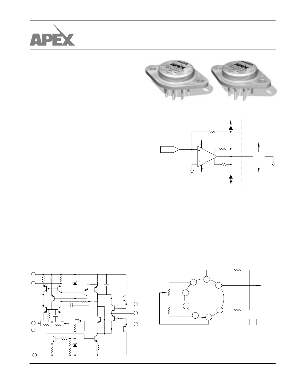
PA08 • PA08A
TYPICAL APPLICATION
+132V
DESCRIPTION
The PA08 is a high voltage operational amplifier designed
for output voltage swings of up to ±145V with a dual (±) supply
or 290V with a single supply. High accuracy is achieved with
a cascode input circuit configuration. All internal biasing is
referenced to a zener diode fed by a FET constant current
source. As a result, the PA08 features an unprecedented
supply range and excellent supply rejection. The output
stage is biased-on for linear operation. Internal phase compensation assures stability at all gain settings. The safe
operating area (SOA) can be observed with all types of loads
by choosing the appropriate current limiting resistors. For
operation into inductive loads, two external flyback pulse
protection diodes are recommended. A heatsink may be
necessary to maintain the proper case temperature under
normal operating conditions.
This hybrid integrated circuit utilizes beryllia (BeO) substrate, thick film resistors, ceramic capacitors and semiconductor chips to maximize reliability, minimize size and give
top performance. Ultrasonically bonded aluminum wires provide reliable interconnections at all operating temperatures.
The 8-pin TO-3 package is hermetically sealed and electrically isolated. The use of compressible thermal isolation
washers and/or improper mounting torque will void the product warranty. Please see “General Operating Considerations”.
EQUIVALENT SCHEMATIC
3
110K
DAC
±1mA
+132V
PA08
-132V
8.2Ω
8.2Ω
-132V
+V
S
D.U.T.
-V
S
ATE PIN DRIVER
The PA08 as a pin driver is capable of supplying high test
voltages to a device under test (DUT). Due to the possibility of
short circuits to any terminal of the DUT, current limit must be
set to be safe when limiting with a supply to output voltage
differential equal to the amplifier supply plus the largest
magnitude voltage applied to any other pin of the DUT. In
addition, flyback diodes are recommended when the output of
the amplifier exits any equipment enclosure to prevent damage due to electrostatic discharges. Refer to Application Note
7 for details on accuracy considerations of this circuit.
EXTERNAL CONNECTIONS
7
Q1
Q5
Q8
5
Q12A Q12B
4
6
APEX MICROTECHNOLOGY CORPORATION • TELEPHONE (520) 690-8600 • FAX (520) 888-3329 • ORDERS (520) 690-8601 • EMAIL prodlit@apexmicrotech.com
C4
Q15
Q2
Q9
D1
Q3
Q4
C3
C2
Q10
D2
Q11
Q16
C1
Q6
2
Q7
1
Q19
8
Q17
PA08 • PA08A
ABSOLUTE MAXIMUM RATINGS
SPECIFICATIONS
ABSOLUTE MAXIMUM RATINGS
SUPPLY VOLTAGE, +VS to –V
OUTPUT CURRENT, within SOA 200mA
S
300V
POWER DISSIPATION, internal at TC = 25°C 17.5W
INPUT VOLTAGE, differential ±50V
INPUT VOLTAGE, common mode ±V
TEMPERATURE, pin solder - 10s max 300°C
TEMPERATURE, junction
1
S
200°C
TEMPERATURE RANGE, storage –65 to +150°C
OPERATING TEMPERATURE RANGE, case –55 to +125°C
SPECIFICATIONS
PARAMETER TEST CONDITIONS
PA08
2
MIN TYP MAX MIN TYP MAX UNITS
PA08A
INPUT
OFFSET VOLTAGE, initial TC = 25°C ±.5 ±2 ±.25 ±.5 mV
OFFSET VOLTAGE, vs. temperature TC = –25°C to +85°C ±15 ±30 ±5 ±10 µV/°C
OFFSET VOLTAGE, vs. supply TC = 25°C ±.5 * 2 µV/V
OFFSET VOLTAGE, vs. time TC = 25°C ±75 * µV/√kh
BIAS CURRENT, initial
BIAS CURRENT, vs. supply TC = 25°C .01 * pA/V
OFFSET CURRENT, initial
INPUT IMPEDANCE, DC TC = 25°C10
3
3
TC = 25°C550310pA
TC = 25°C ±2.5 ±50 ±1.5 ±10 pA
5
*MΩ
INPUT CAPACITANCE TC = 25°C4*pF
COMMON MODE VOLTAGE RANGE4TC = –25°C to +85°C ±VS–10 * V
COMMON MODE REJECTION, DC TC = –25°C to +85°C, VCM = ±90V 130 * dB
GAIN
OPEN LOOP GAIN at 10Hz TC = 25°C, RL = ∞ 118 * dB
OPEN LOOP GAIN at 10Hz TC = 25°C, RL = 1.2KΩ 96 111 * * dB
GAIN BANDWIDTH PRODUCT at 1MHz TC = 25°C, RL = 1.2KΩ 5 * MHz
POWER BANDWIDTH TC = 25°C, RL = 1.2KΩ 90 * kHz
PHASE MARGIN TC = –25 to +85°C60*°
OUTPUT
VOLTAGE SWING
VOLTAGE SWING
VOLTAGE SWING
4
4
4
TC = 25°C, IO = 150mA ±VS–15 ±VS–8 * * V
TC = –25o C to +85oC, IO = ±75mA ±VS–10 ±VS–5 * * V
TC = –25o C to +85oC, IO = ±20mA ±VS–5 ±VS–3 * * V
CURRENT, peak TC = 85°C 150 * mA
SLEW RATE TC = 25°C3020*V/µs
CAPACITIVE LOAD, AV = 1 TC = –25 to +85°C10*nF
CAPACITIVE LOAD, AV > 4 TC = –25 to +85°C SOA *
SETTLING TIME to .1% TC = 25°C, RL= 1.2KΩ, 2V step 1 * µs
POWER SUPPLY
VOLTAGE TC = –55 to +125°C ±15 ±100 ±150 * * * V
CURRENT, quiescent TC = 25°C 6 8.5 * * mA
THERMAL
RESISTANCE, AC junction to case
5
TC = –55 to +125°C, F > 60Hz 3.8 * °C/W
RESISTANCE, DC junction to case TC = –55 to +125°C, F < 60Hz 6.0 6.5 * * °C/W
RESISTANCE, junction to air TC = –55 to +125°C30*°C/W
TEMPERATURE RANGE, case Meets full range specification –25 85 * * °C
NOTES: * The specification of PA08A is identical to the specification for PA08 in applicable column to the left.
1. Long term operation at the maximum junction temperature will result in reduced product life. Derate power dissipation to
achieve high MTTF.
2. The power supply voltage specified under typical (TYP) applies unless otherwise noted.
3. Doubles for every 10oC of temperature increase.
4. +VS and –VS denote the positive and negative supply rail respectively.
5. Rating applies only if output current alternates between both output transistors at a rate faster than 60Hz.
CAUTION
APEX MICROTECHNOLOGY CORPORATION • 5980 NORTH SHANNON ROAD • TUCSON, ARIZONA 85741 • USA • APPLICATIONS HOTLINE: 1 (800) 546-2739
The internal substrate contains beryllia (BeO). Do not break the seal. If accidentally broken, do not crush, machine, or
subject to temperatures in excess of 850°C to avoid generating toxic fumes.

TYPICAL PERFORMANCE
GRAPHS
PA08 • PA08A
30
POWER DERATING
25
20
15
10
5
0
0 25 50 75 100 125
INTERNAL POWER DISSIPATION, P(W)
120
100
(dB)
OL
80
TEMPERATURE, T(°C)
SMALL SIGNAL RESPONSE
R =1.2KLΩ
60
40
20
0
OPEN LOOP GAIN, A
-20
1 100 10M
10 1K 10K .1M 1M
FREQUENCY, F (Hz)
150
250
200
LIM
CURRENT LIMIT
R = 4.7CLΩ
150
100
R = 10CLΩ
CURRENT LIMIT, I (A)
50
0
-25 25 50 75
-55 0 100
CASE TEMPERATURE, T (°C)
PHASE RESPONSE
0
–30
–60
–90
–120
PHASE, (°)ϕ
–150
–180
–210
10 10K 1M
0 100 .1M 10M
1K
FREQUENCY, F (Hz)
C
R =1.2KLΩ
125
OPEN LOOP GAIN
6
4
T = 85°C
C
2
T = -25°C
0
T = -25°C
C
C
R =1.2KLΩ
–2
–4
–6
RELATIVE OPEN LOOP GAIN, A (dB)
100 150 200
30
50
TOTAL SUPPLY VOLTAGE, V (V)
POWER RESPONSE
300
PP
200
O
100
60
OUTPUT VOLTAGE, V (V )
15
|+V | + |–V | = 300V
SS
|+V | + |–V | = 100V
SS
30
50K .1M .3M
.2M
FREQUENCY, F (Hz)
.5M
250
.7M
300
S
1M
PULSE RESPONSE
6
4
o
2
0
–2
–4
OUTPUT VOLTAGE, V (V)
–6
140
V = ±5V, t = 100ns
IN r
0.5 30
1 2.5
1.5
TIME, t (µs)
2.0
COMMON MODE REJECTION
120
100
80
60
40
20
0
1 100 1K 1M
COMMON MODE REJECTION CMR (dB)
10 10K .1M
FREQUENCY, F (Hz)
1.6
1.4
1.2
1.0
SLEW RATE
R =1.2KLΩ
.8
20
√
15
N
10
6
4
.6
NORMALIZED SLEW RATE (X)
.4
50 100 150 200 250 300
TOTAL SUPPLY VOLTAGE, V (V)
POWER SUPPLY REJECTION
140
120
S
2
INPUT NOISE VOLTAGE, V (nV/ Hz)
10 100 10K .1M
FREQUENCY, F (Hz)
COMMON MODE VOLTAGE
300
|+V | + |–V | = 300V
200
CM
SS
100
80
+V
S
60
40
–V
S
20
0
11M
POWER SUPPLY REJECTION, PSR (dB)
10 100 1K 10K .1M
FREQUENCY, F (Hz)
100
60
|+V | + |–V | = 100V
SS
30
15
COMMON MODE VOLTAGE, V (Vpp)
10K 50K .2M
20K 1M
FREQUENCY, F (Hz)
INPUT NOISE
1K
.1M
.5M
APEX MICROTECHNOLOGY CORPORATION • TELEPHONE (520) 690-8600 • FAX (520) 888-3329 • ORDERS (520) 690-8601 • EMAIL prodlit@apexmicrotech.com

PA08 • PA08A
OPERATING
CONSIDERATIONS
GENERAL
Please read the “General Operating Considerations”, which
covers stability, supplies, heatsinking, mounting, current limit,
SOA interpretation, and specification interpretation. Additional
information can be found in the application notes. For information on the package outline, heatsinks, and mounting hardware,
see the “Package Outlines” and “Accessories” sections of the
handbook.
SAFE OPERATING AREA (SOA)
The output stage of most power amplifiers has two distinct
limitations:
1. The current handling capability of the transistor geometry
and the wire bonds.
2. The second breakdown effect which occurs whenever the
simultaneous collector current and collector-emitter voltage
exceeds specified limits.
200
150
100
80
S
50
S
40
+V OR –V (mA)
30
OUTPUT CURRENT FROM
20
80 100 120 150 170
SUPPLY TO OUTPUT DIFFERENTIAL VOLTAGE (V)
t = 1ms
t = 5ms
steady state
The SOA curves combine the effect of these limits. For a
given application, the direction and magnitude of the output
current should be calculated or measured and checked against
the SOA curves. This is simple for resistive loads but more
complex for reactive and EMF generating loads. However, the
following guidelines may save extensive analytical efforts.
1. Under transient conditions, the following capacitive and
inductive loads are safe with the current limits set to the
maximum:
t = 0.5ms
200
t = 200µs
250 300
3. The output stage is protected against transient flyback.
However, for protection against sustained, high energy
flyback, external fast-recovery diodes should be used.
INDUCTIVE LOADS
Two external diodes as shown in Figure 1, are required to
protect these amplifiers from flyback (kickback) pulses
exceeding the supply voltages of the amplifier when driving
inductive loads. For component selection, these external
diodes must be very quick, such as ultra fast recovery diodes
with no more than 200 nanoseconds of reverse recovery time.
The diode will turn on to divert the flyback energy into the supply
rails thus protecting the output transistors from destruction due
to reverse bias.
A note of caution about the supply. The energy of the flyback
pulse must be absorbed by the power supply. As a result, a
transient will be superimposed on the supply voltage, the
magnitude of the transient being a function of its transient
impedance and current sinking capability. If the supply voltage
plus transient exceeds the maximum supply rating or if the AC
impedance of the supply is unknown, it is best to clamp the
output and the supply with a zener diode to absorb the transient.
INPUT PROTECTION
The input is protected against common mode voltages up to
the supply rails and differential voltages up to ±50V. Increased
protection against differential input voltages can be obtained by
adding 2 resistors, 2 capacitors and 4 diode connected FETs
as shown in Figure 2.
Fig. 1 Fig. 2
+V
S
IN4936 OR
UES1106
–V
S
PROTECTION, INDUCTIVE LOAD
+IN
–IN
100pf/200V
150KΩ
Q1
Q2
150KΩ
100pf/200V
PROTECTION, OVERVOLTAGE
_
Q3
Q4
+
±V
S
150V .4µF 280mH
125V .9µF 380mH
100V 2µF 500mH
75V 10µF 1200mH
50V 100µF 13H
2. The amplifier can handle any EMF generating or reactive
C(MAX) L(MAX)
CURRENT LIMITING
Proper operation requires the use of two current limit resistors, connected as shown in the external connection diagram.
The minimum value for R
reliability it should be set as high as possible. Refer to the
“General Operating Considerations” section of the handbook
for current limit adjust details.
is 3.24Ω. However, for optimum
CL
load and short circuits to the supply rails or simple shorts to
common if the current limits are set as follows:
±V
SHORT TO ±V
S
C, L, OR EMF LOAD COMMON
SC,
SHORT TO
150V 20mA 67mA
125V 27mA 90mA
100V 42mA 130mA
75V 67mA 200mA
50V 130mA 200mA
These simplified limits may be exceeded with further analysis
using the operating conditions for a specific application.
This data sheet has been carefully checked and is believed to be reliable, however, no responsibility is assumed for possible inaccuracies or omissions. All specifications are subject to change without notice.
PA08U REV. I FEBRUARY 1998 © 1998 Apex Microtechnology Corp.
 Loading...