

MICROTECHNOLOGY
POWER OPERATIONAL AMPLIFIERS
PA05 • PA05A
HTTP://WWW.APEXMICROTECH.COM (800) 546-APEX (800) 546-2739
FEA TURES
• HIGH INTERNAL DISSIPATION — 250 WATTS
• HIGH VOLTAGE, HIGH CURRENT — 100V, 30A
• HIGH SLEW RATE — 100V/µS
• 4 WIRE CURRENT LIMIT SENSING
• LOW DISTORTION
• EXTERNAL SHUTDOWN CONTROL
• OPTIONAL BOOST VOLTAGE INPUTS
• EVALUATION KIT — SEE EK04
APPLICATIONS
• LINEAR AND ROTARY MOTOR DRIVES
• SONAR TRANSDUCER DRIVER
• YOKE/MAGNETIC FIELD EXCITATION
• PROGRAMMABLE POWER SUPPLIES TO ±45V
• AUDIO UP TO 500W
DESCRIPTION
The PA05 is a high voltage MOSFET power operational
amplifier that extends the performance limits of power amplifiers in slew rate and power bandwidth, while maintaining high
current and power dissipation ratings.
The PA05 is a highly flexible amplifier. The shutdown control
feature allows the output stage to be turned off for standby
operation or load protection during fault conditions. Boost
voltage inputs allow the small signal portion of the amplifier to
operate at a higher voltage than the high current output stage.
The amplifier is then biased to achieve close linear swings to
the supply rails at high currents for extra efficient operation.
External compensation tailors slew rate and bandwidth performance to user needs. A four wire sense technique allows
precision current limiting without the need to consider internal
or external milliohm parasitic resistance in the output line. The
output stage is protected by thermal limiting circuits above
junction temperatures of 175°C.
PA05A
∆
USA BeO
TE949311
The JEDEC MO-127 12-pin Power Dip™ package (see
Package Outlines) is hermetically sealed and isolated from
the internal circuits. The use of compressible thermal washers
and/or improper mounting torque will void the product warranty. Please see “General Operating Considerations”.
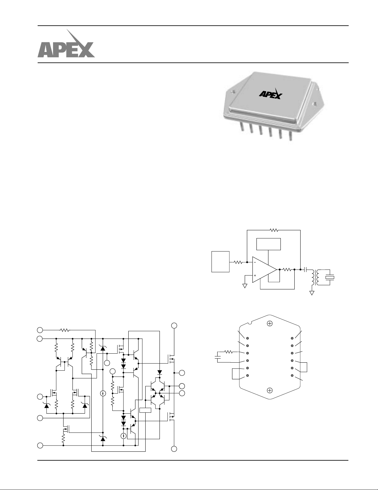
TYPICAL APPLICATION
The high power bandwidth of the PA05 allows driving sonar
transducers via a resonant circuit including the transducer and
a matching transformer. The load circuit appears resistive to
the PA05. Control logic turns off the amplifier's output during
shutdown.
R
f
CONTROL
LOGIC
ULTRA-
SONIC
DRIVE
R
i
1
12
7
R
11
CL
TRANSFORMER
TUNED
2
PA05
10
EQUIVALENT SCHEMATIC
SHUTDOWN
12
9
+V
BOOST
Q1
Q12 Q13
Q16
–IN
1
D19
+IN
2
Q17
D20
Q30
D1
4
Q8
COMP
3
D27
D31
D6
D9
Q10
Q22
Q25
Q33
Q4
Q14
BIAS
Q24
+Vs
D5
Q21
Q18
8
Q5
OUT
I
LIM
I
LIM
Q29
7
11
10
EXTERNAL CONNECTIONS
–INPUT
+INPUT
COMP
R
C
C
COMP
–V
BOOST
–SUPPLY
*
Gain C
1 470pF 120Ω
>3 220pF 120Ω
1
2
3
TOP
C
TOP
VIEW
VIEW
4
5
6
PHASE COMPENSATION
SHUTDOWN
12
11
10
CURRENT LIMIT
CURRENT LIMIT
9
8
7
+V
BOOST
*
+SUPPLY
OUTPUT
C
R
C
≥10 82pF 120Ω
–V
BOOST
5
APEX MICROTECHNOLOGY CORPORATION • TELEPHONE (520) 690-8600 • FAX (520) 888-3329 • ORDERS (520) 690-8601 • EMAIL prodlit@apexmicrotech.com
D4
C
RATED FOR FULL SUPPLY VOLTAGE
6
–Vs
C
*See
BOOST OPERATION
paragraph.
P A05 • P A05A
ABSOLUTE MAXIMUM RATINGS
SPECIFICATIONS
ABSOLUTE MAXIMUM RATINGS
SUPPLY VOLTAGE, +VS to –V
BOOST VOLTAGE SUPPLY VOLTAGE +20V
S
100V
OUTPUT CURRENT, continuous within SOA 30A
POWER DISSIPATION, internal 250W
INPUT VOLTAGE, differential ±20V
INPUT VOLTAGE, common mode ±V
TEMPERATURE, pin solder - 10s 300°C
TEMPERATURE, junction
2
B
175°C
TEMPERATURE, storage –65 to +150°C
OPERATING TEMPERATURE RANGE, case –55 to +125°C
SPECIFICATIONS
PARAMETER TEST CONDITIONS
PA05
1
MIN TYP MAX MIN TYP MAX UNITS
PA05A
INPUT
OFFSET VOLTAGE, initial 5 10 2 5 mV
OFFSET VOLTAGE, vs. temperature Full temperature range 20 50 10 30 µV/°C
OFFSET VOLTAGE, vs. supply 10 30 * * µV/V
OFFSET VOLTAGE, vs. power Full temperature range 30 10 µV/W
BIAS CURRENT, initial 10 50 5 20 pA
BIAS CURRENT, vs. supply .01 * pA/V
OFFSET CURRENT, initial 10 50 5 20 pA
INPUT IMPEDANCE, DC 10
11
* Ω
INPUT CAPACITANCE 13 * pF
COMMON MODE VOLTAGE RANGE Full temperature range ±VB–8 * V
COMMON MODE REJECTION, DC Full temp. range, VCM = ±20V 90 100 * * dB
INPUT NOISE 100KHz BW, RS = 1KΩ 10 * µVrms
GAIN
OPEN LOOP, @ 15Hz Full temperature range, CC = 82pF 94 102 * * dB
GAIN BANDWIDTH PRODUCT RL = 10Ω 3 * MHz
POWER BANDWIDTH RL = 4Ω, VO = 80V
CC = 82pF, RC = 120Ω
, AV = –10 400 * kHz
P-P
PHASE MARGIN Full temperature range, CC = 470pF 60 * °
OUTPUT
VOLTAGE SWING IO = 20A ±VS–9.5 ±VS–8.7 * * V
VOLTAGE SWING V
CURRENT, peak 30 * A
= Vs + 5V, IO = 30A ±VS–5.8 ±VS–5.0 * * V
BOOST
SETTLING TIME to .1% AV = +1, 10V step, RL = 4Ω 2.5 * µs
SLEW RATE AV = –10, CC = 82pF, RC = 120Ω 80 100 * V/µs
CAPACITIVE LOAD Full temperature range, AV = +1 2.2 * n F
RESISTANCE IO = 0, No load, 2MHz 5 * Ω
IO = 1A, 2MHz 2 * Ω
POWER SUPPLY
VOLTAGE Full temperature range ±15 ±45 ±50 * * * V
CURRENT, quiescent, boost supply 46 56 * * mA
CURRENT, quiescent, total 90 120 * * mA
CURRENT, quiescent, total, shutdown 46 56 * * mA
THERMAL
RESISTANCE, AC, junction to case
RESISTANCE, DC, junction to case Full temperature range, F<60Hz .4 .5 * * °C/W
RESISTANCE, junction to air
3
Full temperature range, F>60Hz .3 .4 * * °C/W
4
Full temperature range 12 * °C/W
TEMPERATURE RANGE, case Meets full range specification –25 85 * * °C
NOTES: * The specification of PA05A is identical to the specification for PA05 in applicable column to the left.
1. Unless otherwise noted: TC = 25°C, CC = 470pF, RC = 120 ohms. DC input specifications are ± value given. Power supply
voltage is typical rating. ±V
2. Long term operation at the maximum junction temperature will result in reduced product life. Derate internal power dissipation
BOOST
= ±VS.
to achieve high MTTF. For guidance, refer to the heatsink data sheet.
3. Rating applies if the output current alternates between both output transistors at a rate faster than 60 Hz.
4. The PA05 must be used with a heatsink or the quiescent power may drive the unit to junction temperatures higher than 150°C.
CAUTION
The PA05 is constructed from MOSFET transistors. ESD handling procedures must be observed.
The internal substrate contains beryllia (BeO). Do not break the seal. If accidentally broken, do not crush, machine, or
subject to temperatures in excess of 850°C to avoid generating toxic fumes.
APEX MICROTECHNOLOGY CORPORATION • 5980 NORTH SHANNON ROAD • TUCSON, ARIZONA 85741 • USA • APPLICATIONS HOTLINE: 1 (800) 546-2739

TYPICAL PERFORMANCE
GRAPHS
P A05 • PA05A
250
POWER DERATING
200
150
100
50
0
0 25 50 75 100 125 150
INTERNAL POWER DISSIPATION, P(W)
CASE TEMPERATURE, T(°C)
SMALL SIGNAL RESPONSE
100
R = 8
Ω
L
80
R = 120
Ω
C
CC = 82pf
60
CC = 220pf
40
CC = 470pf
20
OPEN LOOP GAIN, A(dB)
0
100 10M
10 1K 10K 100K 1M
FREQUENCY, f (Hz)
POWER SUPPLY REJECTION
100
80
60
40
20
0
100 1K 10M
10 10K 100K 1M
POWER SUPPLY REJECTION, PSR (dB)
0
FREQUENCY f (Hz)
PHASE RESPONSE
CC = 82pf
–45
–90
Φ
CC = 470pf
–135
PHASE, (°)
–180
R = 8
L
R = 120
–225
C
100 10M10 1K 10K 100K 1M
CC = 220pf
Ω
Ω
CC = 470pf
CC = 220pf
CC = 82pf
FREQUENCY, f (Hz)
SLEW RATE VS. COMP.
100
80
60
40
SLEW RATE, SR (V/µs)
20
100 200
EXT. COMPENSATION CAPACITOR C (pF)
OUTPUT VOLTAGE SWING
(V)
O
12
–V
S
10
8
6
4
2
0 5 20 30
OUTPUT CURRENT, I (A)
VOLTAGE DROP FROM SUPPLY, V
300 400 500
S
BOOST
V = V
+ 5V
V = V
15
10 25
S
BOOST
O
C
COMMON MODE REJECTION
100
80
60
40
20
0
10
COMMON MODE REJECTION, CMR (dB)
.2
.1
.05
FREQUENCY, f (Hz)
HARMONIC DISTORTION
A = 10
V
R = 2
Ω
L
C = 82pF, R = 120
C
±Vs = 31V
.02
.01
.005
DISTORTION, THD (%)
.002
.001
30 300 30K
100 1K 3K 10K
FREQUENCY, f (Hz)
10K 100K
C
P = 1W
O
Ω
O
P = 300W
O
P = 200W
7.5
PULSE RESPONSE
A = +1
5
O
2.5
0
–2.5
–5
OUTPUT VOLTAGE, V (V)
1M100 1K 0 10 15
–7.5
TIME, t (µs)
QUIESCENT CURRENT
Q
1.2
1.1
1.0
.9
.8
NORMALIZED QUIESCENT CURRENT, I (X)
40 60 80
20 100
TOTAL SUPPLY VOLTAGE, V (V)
C = 470pF
CV
25
S
30520
130
CURRENT LIMIT
120
110
100
90
80
70
60
NORMALIZED CURRENT LIMIT, (%)
–50 0 75 125
–25 25 100
CASE TEMPERATURE, T (°C)
50
C
POWER RESPONSE
100
)
60
PP
40
O
20
C = 470pF
C
10
6
4
OUTPUT VOLTAGE, V (V
2
100K
40K
FREQUENCY, f (Hz)
C = 220pF
C
.4M
C = 82pF
C
1M
4M
APEX MICROTECHNOLOGY CORPORATION • TELEPHONE (520) 690-8600 • FAX (520) 888-3329 • ORDERS (520) 690-8601 • EMAIL prodlit@apexmicrotech.com

P A05 • PA05A
(V)
OPERATING
CONSIDERATIONS
GENERAL
Please read the
which covers stability, supplies, heatsinking, mounting, current limit, SOA interpretation, and specification interpretation.
Additional information can be found in the application notes.
For information on the package outline, heatsinks, and mounting hardware, consult the
Data
section of the handbook. The EK04 Evaluation Kit makes
prototype circuits a snap by providing an EK04PC proto circuit
board, MS05 mating socket, HS11 heatsink and hardware kit.
General Operating Considerations
Accessory and Package Mechanical
section,
CURRENT LIMIT
The two current limit sense lines are to be connected directly
across the current limit sense resistor.
For the current limit to
work correctly, pin 11 must be connected to the amplifier
output side and pin 10 connected to the load side of the current
limit resistor, RCL, as shown in Figure 1.
This connection will
bypass any parasitic resistances, RP formed by sockets and
solder joints as well as internal amplifier losses. The current
limiting resistor may not be placed anywhere in the output
circuit except where shown in Figure 1. If current limiting is not
used, pins 10 and 11 must be tied to pin 7.
The value of the current limit resistor can be calculated as
follows:
R
INPUT
FIGURE 1. CURRENT LIMIT
10
i
1
PA05
2
CL
R
f
11
7
CL
I
= .7/R
LIMIT
R
R
CL
P
R
L
CL
SAFE OPERATING AREA (SOA)
The MOSFET output stage of this power operational ampli-
fier has two distinct limitations:
1. The current handling capability of the MOSFET geometry
and the wire bonds.
2. The junction temperature of the output MOSFETs.
NOTE: The output stage is protected against transient flyback.
However, for protection against sustained, high energy
flyback, external fast-recovery diodes should be used.
30
15
12
9
6
3
1.5
OUTPUT CURRENT (A)
1.2
.9
.6
.3
1
2510
34 20
SUPPLY TO OUTPUT DIFFERENTIAL
DC Tc = 125°C
t = 200ms
DC Tc = 25°C
DC Tc = 85°C
30
40 50
100
SHUTDOWN OPERATION
To disable the output stage, pin 12 is connected to ground
via relay contacts or via an electronic switch. The switching
device must be capable of sinking 2mA to complete shutdown
and capable of standing off the supply voltage +V
. See Figure
S
2 for suggested circuits.
–LOGIC
A
–LOGIC
B
FIGURE 2. SHUTDOWN OPERATION
470Ω
K1
Q1
12
SHUTDOWN
12
SHUTDOWN
From an internal circuitry standpoint, shutdown is just a
special case of current limit where the allowed output current
is zero. As with current limit, however, a small current does flow
in the output during shutdown. A load impedance of 100 ohms
or less is required to insure the output transistors are turned off.
Note that even though the output transistors are off the output
pin is not open circuited because of the shutdown operating
current.
BOOST OPERATION
With the V
amplifier are operated at higher supply voltages than the
amplifier’s high current output stage. +V
–V
(pin 5) are connected to the small signal circuitry of
BOOST
the amplifier. +V
high current output stage. An additional 5V on the V
is sufficient to allow the small signal stages to drive the output
transistors into saturation and improve the output voltage
swing for extra efficient operation when required. When close
swings to the supply rails is not required the +V
pins must be strapped together as well as the –V
pins. The boost voltage pins must not be at a voltage lower than
the V
pins.
S
feature, the small signal stages of the
BOOST
(pin 9), and
BOOST
(pin 8) and –VS (pin 6) are connected to the
S
BOOST
and +V
BOOST
and –V
BOOST
pins
COMPENSATION
The external compensation components CC and RC are
connected to pins 3 and 4. Unity gain stability can be achieved
at any compensation capacitance greater than 470 pF with at
least 60 degrees of phase margin. At higher gains, more phase
shift can be tolerated in most designs and the compensation
capacitance can accordingly be reduced, resulting in higher
bandwidth and slew rate. Use the typical operating curves as
a guide to select C
and RC for the application.
C
S
S
This data sheet has been carefully checked and is believed to be reliable, however, no responsibility is assumed for possible inaccuracies or omissions. All specifications are subject to change without notice.
PA05U REV. F DECEMBER 1997 © 1997 Apex Microtechnology Corp.
 Loading...