

FEA TURES
HTTP://WWW.APEXMICROTECH.COM (800) 546-APEX (800) 546-2739
MICROTECHNOLOGY
POWER OPERATIONAL AMPLIFIERS
PA02 • PA02A
• HIGH POWER BANDWIDTH — 350kHz
• HIGH SLEW RATE — 20V/µs
• FAST SETTLING TIME — 600ns
• LOW CROSSOVER DISTORTION — Class A/B
• LOW INTERNAL LOSSES — 1.2V at 2A
• HIGH OUTPUT CURRENT — ±5A PEAK
• LOW INPUT BIAS CURRENT — FET Input
• ISOLATED CASE — 300 VDC
APPLICATIONS
• MOTOR, VALVE AND ACTUATOR CONTROL
• MAGNETIC DEFLECTION CIRCUITS UP TO 5A
• POWER TRANSDUCERS UP TO 350 kHz
• AUDIO AMPLIFIERS UP TO 30W RMS
DESCRIPTION
The PA02 and PA02A are wideband, high output current
operational amplifiers designed to drive resistive, inductive
and capacitive loads. Their complementary “collector output”
stage can swing close to the supply rails and is protected
against inductive kickback. For optimum linearity, the output
stage is biased for class A/B operation. The safe operating
area (SOA) can be observed for all operating conditions by
selection of user programmable, current limiting resistors
(down to 10mA). Both amplifiers are internally compensated
but are not recommended for use as unity gain followers. For
continuous operation under load, mounting on a heatsink of
proper rating is recommended.
These hybrid integrated circuits utilize thick film (cermet)
resistors, ceramic capacitors and semiconductor chips to
maximize reliability, minimize size and give top performance.
Ultrasonically bonded aluminum wires provide reliable interconnections at all operating temperatures. The 8-pin TO-3
package is hermetically sealed and electrically isolated.
Isolation washers are not recommended. The use of compressible thermal washers and/or improper mounting torque
will void the product warranty. Please see “General Operating Considerations”.
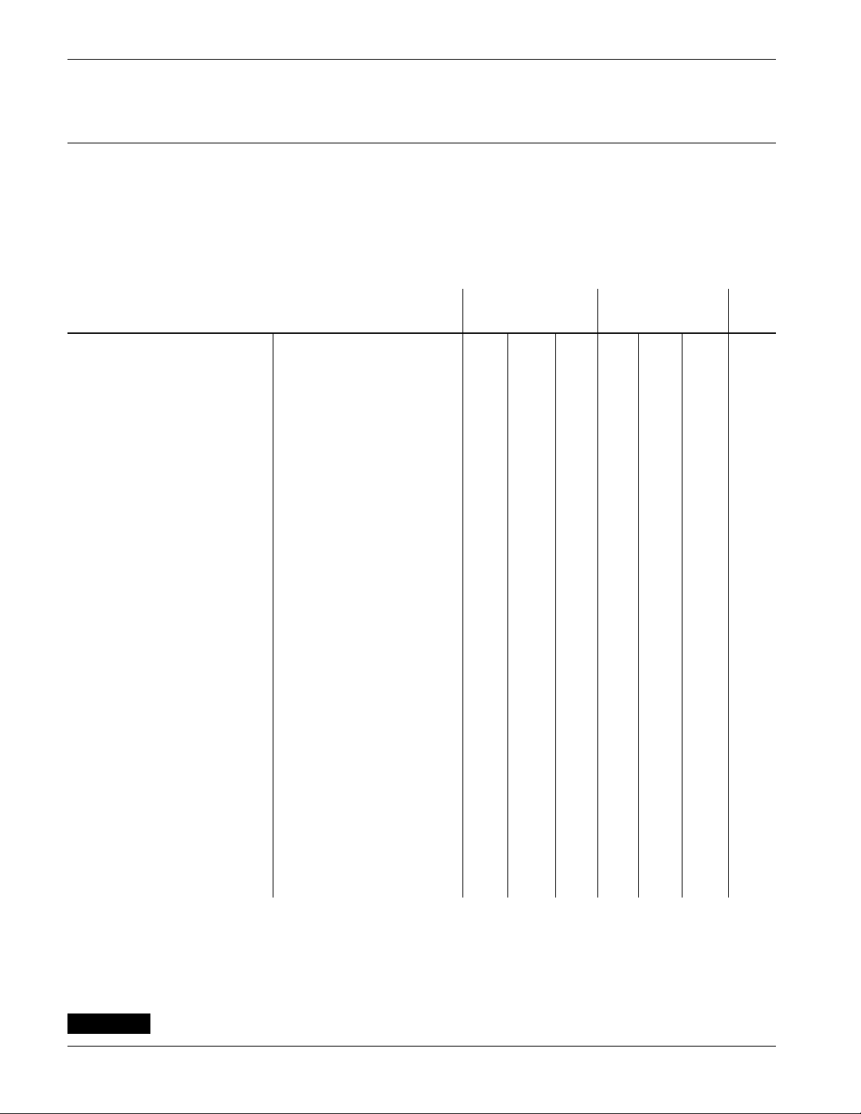
EQUIVALENT SCHEMATIC
2
R1
R2 R3
R4
6
5
R8
R9 R10
R11
7
R5
Q2
A1
Q7
R12
Q1
Q8
R15
R6
R13
Q4
Q5
R7
Q3
Q6
R14
APEX MICROTECHNOLOGY CORPORATION • TELEPHONE (520) 690-8600 • FAX (520) 888-3329 • ORDERS (520) 690-8601 • EMAIL prodlit@apexmicrotech.com
D1
1
3
4
8
D2
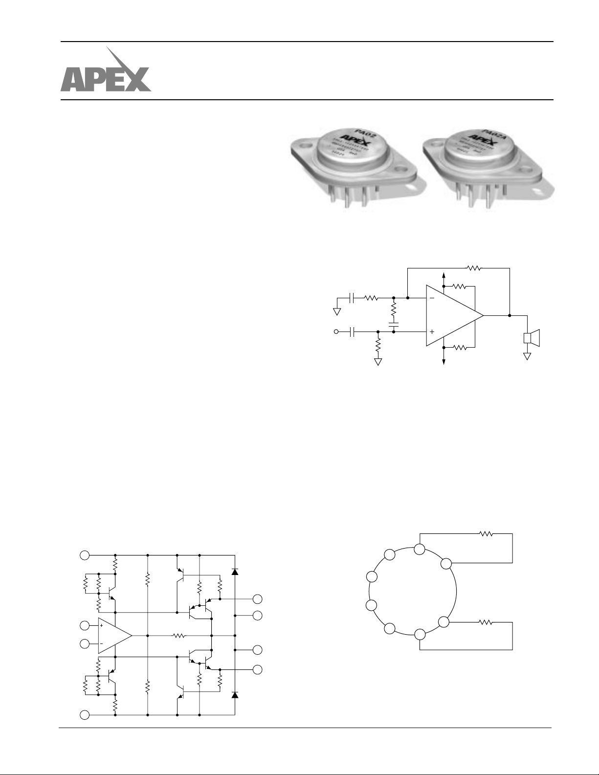
TYPICAL APPLICATION
Vehicular Sound System Power Stage
100K
+12
R
PA02
.27
R
.27
CL+
CL–
Ω
3.2
Ω
16W
Ω
.47µF
16K
1K
IN
.001µF
.47µF
LOW INTERNAL LOSS MAXIMIZES EFFICIENCY
16K
–12
When system voltages are low and power is at a premium,
the PA02 is a natural choice. The circuit above utilizes not only
the feature of low internal loss of the PA02, but also its very low
distortion level to implement a crystal clear audio amplifier
suitable even for airborne applications. This circuit uses AC
coupling of both the input signal and the gain circuit to render
DC voltage across the speaker insignificant. The resistor and
capacitor across the inputs form a stability enhancement
network. The 0.27 ohm current limit resistors provide protection in the event of an output short circuit.
EXTERNAL CONNECTIONS
R
CL+
+V
S
2
TOP VIEW
7
–V
S
1
8
CL–
CL+
R
CL–
OUT
–IN
OUT
4
5
+IN
3
6
P A02 • P A02A
ABSOLUTE MAXIMUM RATINGS
SPECIFICATIONS
ABSOLUTE MAXIMUM RATINGS
SUPPLY VOLTAGE, +VS to –V
OUTPUT CURRENT, within SOA 5A
POWER DISSIPATION, internal
S
1
38V
48W
INPUT VOLTAGE, differential ±VS –5V
INPUT VOLTAGE, common mode ±VS –2V
TEMPERATURE, pin solder - 10s 300°C
TEMPERATURE, junction
1
150°C
TEMPERATURE RANGE, storage –65 to +150°C
OPERATING TEMPERATURE RANGE, case –55 to +125°C
SPECIFICATIONS
PARAMETER TEST CONDITIONS
PA02
2, 6
MIN TYP MAX MIN TYP MAX UNITS
PA02A
INPUT
OFFSET VOLTAGE, initial TC = 25°C ±5 ±10 ±1 ±3mV
OFFSET VOLTAGE, vs. temperature Full temperature range ±10 ±50 * ±25 µV/°C
OFFSET VOLTAGE, vs. supply TC = 25°C ±10 * µV/V
OFFSET VOLTAGE, vs. power TC = 25°C ±6*µV/W
BIAS CURRENT, initial TC = 25°C 50 200 25 100 pA
BIAS CURRENT, vs. temperature TC = 85°C 200 * pA/°C
BIAS CURRENT, vs. supply TC = 25°C .01 * pA/V
OFFSET CURRENT, initial TC = 25°C 25 100 15 50 pA
OFFSET CURRENT, vs. temperature TC = 85°C 100 * pA/°C
INPUT IMPEDANCE, DC TC = 25°C 1000 * GΩ
INPUT CAPACITANCE TC = 25°C3*pF
COMMON MODE VOLT. RANGE5, Pos. Full temperature range +VS –6 +VS –3 * * V
COMMON MODE VOLT. RANGE5, Neg. Full temperature range –VS +6 –VS +5 * * V
COMMON MODE REJECTION, DC Full temperature range 70 100 * * dB
GAIN
OPEN LOOP GAIN at 10Hz TC = 25°C, 1kΩ load 103 * dB
OPEN LOOP GAIN at 10Hz Full temp. range, 10kΩ load 86 100 * * dB
GAIN BANDWIDTH PRODUCT at 1MHz TC = 25°C, 10Ω load 4.5 * MHz
POWER BANDWIDTH TC = 25°C, 10Ω load 350 * kHz
PHASE MARGIN Full temp. range, 10Ω load 30 * °
OUTPUT
VOLTAGE SWING
VOLTAGE SWING
3
3
TC = 25°C, IO = 5A, R
Full temp. range, IO = 2A ±VS –2 ±VS –1.2 * * V
= .08Ω±V
CL
–4 ±VS –3 * * V
S
CURRENT, peak TC = 25°C5*A
SETTLING TIME to .1% TC = 25°C, 2V step .6 * µs
SLEW RATE TC = 25°C1320**V/µs
CAPACITIVE LOAD Full temp. range, AV > 10 SOA *
HARMONIC DISTORTION PO = .5W, F = 1kHz, RL = 10Ω .004 * %
SMALL SIGNAL rise/fall time RL = 10Ω, AV = 1 100 * ns
SMALL SIGNAL overshoot RL = 10Ω, AV = 1 10 * %
POWER SUPPLY
VOLTAGE Full temperature range ±7 ±15 ±19 * * * V
CURRENT, quiescent TC = 25°C2740**mA
THERMAL
RESISTANCE, AC junction to case
4
F > 60Hz 1.9 2.1 * * °C/W
RESISTANCE, DC junction to case F < 60Hz 2.4 2.6 * * °C/W
RESISTANCE, junction to air 30 * °C/W
TEMPERATURE RANGE, case Meets full range specifications –25 +85 –55 +125 °C
NOTES: * The specification of PA02A is identical to the specification for PA02 in applicable column to the left.
1. Long term operation at the maximum junction temperature will result in reduced product life. Derate internal power dissipation
to achieve high MTTF.
2. The power supply voltage for all specifications is the TYP rating unless otherwise noted as a test condition.
3. +VS and –VS denote the positive and negative supply rail respectively. Total VS is measured from +VS to –VS.
4. Rating applies if the output current alternates between both output transistors at a rate faster than 60Hz.
5. Exceeding CMV range can cause the output to latch.
6. Full temperature specifications are guaranteed but not 100% tested.
CAUTION
The internal substrate contains beryllia (BeO). Do not break the seal. If accidentally broken, do not crush, machine, or
subject to temperatures in excess of 850°C to avoid generating toxic fumes.
APEX MICROTECHNOLOGY CORPORATION • 5980 NORTH SHANNON ROAD • TUCSON, ARIZONA 85741 • USA • APPLICATIONS HOTLINE: 1 (800) 546-2739

TYPICAL PERFORMANCE
GRAPHS
P A02 • P A02A
50
POWER DERATING
40
T=T
C
30
20
10
T=T
A
0
0 25 50 75 100 125
INTERNAL POWER DISSIPATION, P(W)
120
100
(dB)
OL
80
TEMPERATURE, T (°C)
SMALL SIGNAL RESPONSE
60
40
20
0
OPEN LOOP GAIN, A
–20
10 1K 10K .1M 1M
1 100 10M
FREQUENCY, F (Hz)
150
OUTPUT VOLTAGE SWING
3.5
(V)
O
3.0
–V
S
2.5
TC = 25 to 85°C
2.0
1.5
±V
O
1.0
.5
SATURATION VOLTAGE, V
12345
0
OUTPUT CURRENT, I
PHASE RESPONSE
0
–30
–60
Φ
–90
–120
PHASE, (°)
–150
–180
–210
10 10K 1M
1 100 .1M 10M
1K
FREQUENCY, F (Hz)
3.0
CURRENT LIMIT
2.5
LIM
2.0
RCL = 0.3
1.5
R
= 0.62ΩΩ
1.0
.5
CURRENT LIMIT, I (A)
0
–25 50 100
(A)
O
025 75
CASE TEMPERATURE, T (°C)
POWER RESPONSE
30
CL
125
C
| +VS | + | –VS | = 36V
PP
23
O
18
| + | –VS | = 30V
| +V
S
13
10
7.8
OUTPUT VOLTAGE, V (V )
6
.1M .2M .5M 1M
.3M
.7M
FREQUENCY, F (Hz)
BIAS CURRENT
B
256
64
16
4
1
.25
.06
NORMALIZED BIAS CURRENT, I (X)
√
(nV/ Hz)
n
5456585
–15 105
40
25
CASE TEMPERATURE, T (°C)
C
INPUT NOISE
35
30
25
20
15
10
INPUT NOISE VOLTAGE, e
10 100 10K .1M
1K
FREQUENCY, F (Hz)
COMMON MODE REJECTION
120
100
80
60
40
20
1 10K
COMMON MODE REJECTION, CMR (dB)
(X)
Q
1.6
FREQUENCY, F (Hz)
QUIESCENT CURRENT
.1M10 100 1K 1M
1.5
1.4
1.3
1.2
1.1
1.0
.9
0 25 50 75 100
–25 125
CASE TEMPERATURE, T
NORMALIZED QUIESCENT CURRENT, I
(°C)
C
10M
POWER SUPPLY REJECTION
140
120
100
+V
80
S
60
–V
40
S
20
0
10
POWER SUPPLY REJECTION, PSR (dB)
100 1K 10K .1M 1M 10M
FREQUENCY, F(Hz)
3
SETTLING TIME
2.5
2
1mV NO LOAD
1.5
TIME, t (µS)
1
.5
0
134 7
256
10mV NO LOAD
10mV 10 LOAD
Ω
OUTPUT CHANGE FROM ZERO, VOLTS
8
APEX MICROTECHNOLOGY CORPORATION • TELEPHONE (520) 690-8600 • FAX (520) 888-3329 • ORDERS (520) 690-8601 • EMAIL prodlit@apexmicrotech.com

P A02 • PA02A
,
)
OPERATING
CONSIDERATIONS
HARMONIC DISTORTION
1
GAIN = 1
LOAD = 10
.3
.1
.03
.01
DISTORTION, THD (%)
.003
.001
100 1K 3K .1M
300 10K 30K
15
(V)
10
O
5
0
–5
OUTPUT VOLTAGE, V
–10
–15
.3
.2
(V)
O
.1
0
–.1
–.2
OUTPUT VOLTAGE, V
–.3
0
–.3
∆
–.6
–.9
–1.2
DELTA GAIN WITH LOAD, A (dB)
–1.5
Ω
= 50mW
O
P
= .5W
O
P
= 5W
O
P
FREQUENCY, F (Hz)
PULSE RESPONSE
VIN = ±1V, tr = 100ns
LOAD = 10
25
134
0
TIME, t (µS)
Ω
PULSE RESPONSE
VIN = ±.2V, tr = 50ns
0 .5 1.0 1.5
TIME, t (µS)
LOADING EFFECTS
IO = 150mA
= 400mA
I
O
FREQUENCY
10K
F (Hz
.3M
.1M100 1K
GENERAL
Please read the “General Operating Considerations” section which covers stability,
supplies, heatsinking, mounting, current limit, SOA interpretation, and specification
interpretation. Additional information can be found in the application notes. For
information on the package outline, heatsinks, and mounting hardware, consult the
“Accessory and Package Mechanical Data” section of the handbook.
SAFE OPERATING AREA (SOA)
The SOA curves combine the
effect of all limits for this Power
Op Amp. For a given application, the direction and magnitude of the output current should
be calculated or measured and
checked against the SOA
curves. This is simple for resistive loads but more complex for
reactive and EMF generating
loads. The following guidelines
may save extensive analytical
efforts:
1. Under transient conditions,
capacitive and dynamic*
loads up to the following maxi-
5.0
(A)
S
4.0
3.0
2.0
1.5
1.0
0.7
0.5
0.3
0.2
OUTPUT CURRENT FROM +V OR –V
2 3 5 7 10 15 20 25 30 40
SUPPLY TO OUTPUT DIFFERENTIAL VOLTAGE V
T
T
C
= 125°C
T
C
T
C
= 70°C
C
= 100°C
= 25°C
BREAKDOWN
SECOND
STEADY STATE
THERMAL
t = 5ms
–VO (V)
S
mums are safe:
CAPACITIVE LOAD INDUCTIVE LOAD
±V
S
I
= 2A I
LIM
= 5A I
LIM
= 2A I
LIM
LIM
= 5A
18V 2mF 0.7mF .2H 10mH
15V 10mF 2.2mF .7H 25mH
10V 25mF 10mF 5H 50mH
* If the inductive load is driven near steady state conditions, allowing the output voltage to drop more than 8V
below the supply rail with I
limiting, the inductor should be capacitively coupled or the current limit must be lowered to meet SOA criteria.
= 5A, or 17V below the supply rail with I
LIM
= 2A while the amplifier is current
LIM
2. The amplifier can handle any EMF generating or reactive load and short circuits to
the supply rails or shorts to common if the current limits are set as follows at
T
= 85°C.
C
±V
SHORT TO
S
C, L OR EMF LOAD COMMON
±V
S
SHORT TO
18V .5A 1.7A
15V .7A 2.8A
10V 1.6A 4.2A
These simplified limits may be exceeded with further analysis using the operating
conditions for a specific application.
CURRENT LIMIT
Proper operation requires the use of two current limit resistors, connected as shown
in the external connection diagram. The minimum value for R
for optimum reliability it should be set as high as possible. Refer to the “General
Operating Considerations” section of the handbook for current limit adjust details.
is 0.12 ohm, however
CL
DEVICE MOUNTING
The case (mounting flange) is electrically isolated and should be mounted directly to
a heatsink with thermal compound. Screws with Belville spring washers are recommended to maintain positive clamping pressure on heatsink mounting surfaces. Long
periods of thermal cycling can loosen mounting screws and increase thermal resistance.
Since the case is electrically isolated (floating) with respect to the internal circuits it
is recommended to connect it to common or other convenient AC ground potential.
This data sheet has been carefully checked and is believed to be reliable, however, no responsibility is assumed for possible inaccuracies or omissions. All specifications are subject to change without notice.
PA02U REV. L FEBRUARY 1998 © 1998 Apex Microtechnology Corp.
 Loading...