

Page 1

SERVICE MANUAL
FILE NO. SM-CTV-O-044
COLOR TELEVISION
SERVICE MANUAL
MODEL NO.
CHASSIS NO. CH-10C1(S)
AT2408S/AT2408
Please read this manual carefully before service
PRINTED IN CHINA.MAY.2003 ©
Page 2

SERVICE MANUAL
CONTENTS
SAFETY INSTRUCTIONS...........................................................................................1
SPECIFICATIONS .......................................................................................................2
KDEY ICS AND ASSEMBLIES....................................................................................3
SYSTEM BLOCK DIAGRAMS.....................................................................................4
IC DATA AND WAVEFORMS OF KEY POINTS ..........................................................5
CIRCUIT ADJUSTMENTS...........................................................................................5
SET-UP ADJUSTMENTS ............................................................................................5
SERVICE MODE AND BUS DATA ..............................................................................5
TROUBLESHOOTING FLOW CHARTS......................................................................7
SERVICE SPARE PARTS LIST.................................................................................13
APPENDIX
1. CIRCUIT DIAGRAM
2. FINAL WIRING DIAGRAM
3. FINAL ASSEMBLY DIAGRAM
4. PRINTED CIRCUIT BOARD DIAGRAMS
Page 3

SERVICE MANUAL
SAFETY INSTRUCTIONS
WARNING: BEFORE SERVICING THIS CHASSIS, READ THE “X-RAY
RADIATION PRECAUTION”, “SAFETY PRECAUTION” AND “PRODUCT
SAFETY NOTICE” INSTRUCTION BELOW.
X-RAY RADIATION PRECAUTION
1. The EHT must be checked every time the TV is serviced to ensure that the CRT does not emit X-ray
radiation as result of excessive EHT voltage. The nominal EHT for this TV is 27.5KV at zero beam
current (minimum brightness) operating at AC 120V. The maximum EHT voltage permissible in any
operating circumstances must not exceed 30KV. When checking the EHT, use the High Voltage
Check procedure in this manual using an accurate EHT voltmeter.
2. The only source of X-RAY in this TV is the CRT. To prevent X-ray radiation, the replacement CRT
must be identical to the original fitted as specified in the parts list.
3. Some components used in this TV have safety related characteristics preventing the CRT from
emitting X-ray radiation. For continued safety, replacement component should be made after
referring the PRODUCT SAFETY NOTICE below.
SAFETY PRECAUTION
1. The TV has a nominal working EHT voltage of 27.5KV. Extreme caution should be exercised when
working on the TV with the back removed.
1) Do not attempt to service this TV if you are not conversant with the precautions and procedures for
working on high voltage equipment.
2) When handling or working on the CRT, always discharge the anode to the TV chassis before
removing the anode cap in case of electric shock.
3) The CRT, if broken, will violently expel glass fragments. Use shatterproof goggles and take extreme
care while handling.
4) Do not hold the CRT by the neck as this is a very dangerous practice.
2. It is essential that to maintain the safety of the customer all power cord forms be replaced exactly as
supplied from factory.
3. Voltage exists between the hot and cold ground when the TV is in operation. Install a suitable
isolating transformer of beyond rated overall power when servicing or connecting any test
equipment for the sake of safety.
4. Replace blown fuses within the TV with the fuse specified in the parts list.
5. When replacing wires or components to terminals or tags, wind the leads around the terminal before
soldering. When replacing safety components identified by the international hazard symbols in the
circuit diagram and parts list, it must be the company-approved type and must be mounted as the
original.
6. Keep wires away from high temperature components.
1
Page 4
SERVICE MANUAL
r
r
r
r
r
A
SAFETY INSTRUCTIONS (continued)
PRODUCT SAFETY NOTICE
Many electrical and mechanical components in this chassis have special safety-related characteristics.
These characteristics are often passed unnoticed by a visual inspection and the X-ray radiation
protection afforded by them cannot necessarily be obtained by using replacements rated at higher
voltages or wattage, etc. Components which have these special safety characteristics in this manual
and its supplements are identified by the international hazard symbols in the circuit diagram and parts
list. Before replacing any of these components read the parts list in this manual carefully. Substitute
replacement components which do not have the same safety characteristics as specified in the parts
list may create X-ray radiation.
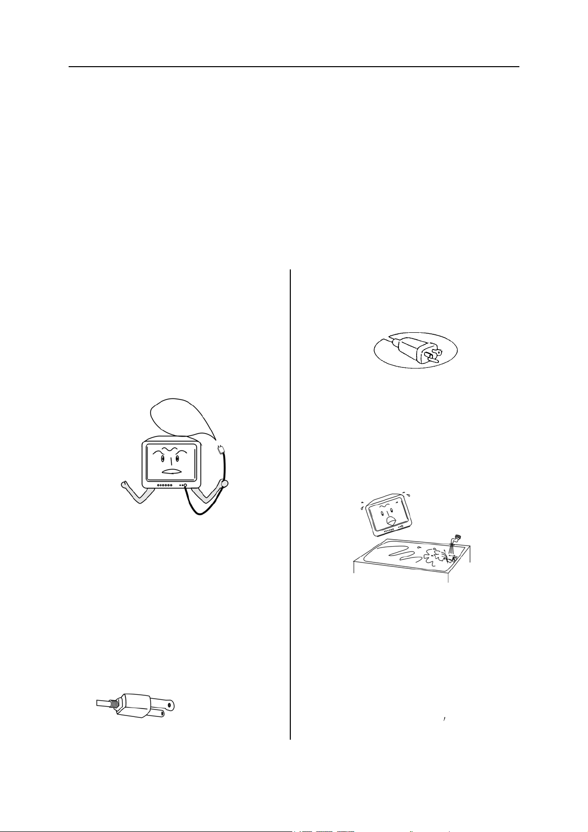
PRECAUTIONS
Power Sources-The TV set should be operated
only from the type of power source indicated on
the TV set or as indicated in the Service
Manual. If you are not sure of the type of powe
supply in your home, consult your sales person
or your local power company. For TV sets
designed to operate from battery power, or othe
sources, refer to the operating instructions.
Grounding or Polarization-Do not defeat the
safety purpose of the polarized o
grounding-type plug. A polarized plug has two
blades with one wider than the other.
grounding-type plug has two blades and a third
grounding prong. The wide blade or the third
prong is provided for your safety. If the provided
plug does not fit into your outlet, consult an
electrician for replacement of the obsolete
outlet.
Wide blade
Lame large
Cuchilla ancha
Alternate Warnings-A three wire grounding type
plug-a plug having a third (grounding) pin. This
plug will only fit into grounding type powe
outlet.
Water and Moisture Warnings-Do not use the
TV set near water-for example, near a bath tub,
wash bowl, kitchen sink, or laundry tub; in a wet
basement; or near a swimming pool; and the
like.The TV set shall not be exposed to dripping
or splashing and no objects filled with liquids,
such as vases, shall be placed on the TV set.
Ventilation-Slots and openings in the cabinet are
provided for ventilation and to ensure reliable
operation of the TV set and to protect it from
overheating, and these openings must not be
blocked or covered. The openings should neve
be blocked by placing the TV set on a bed, sofa,
rug, or other similar surface. This TV set should
not be placed in a built-in installation such as a
bookcase or rack unless proper ventilation is
provided or the manufacturer
have been adhered to.
s instructions
2
Page 5

SERVICE MANUAL
SPECIFICATIONS
Television system:
Channel coverage:
Channels preset:
Antenna input:
Picture tube;
Max. audio output;
Power source;
Weight:
Dimensions(W/H/D):
Packing dimensions(W/H/D):
Rated power consumption:
NTSC-M
VHF 2
UHF 14
CABLE TV: MID BAND (A-8
13
69
A-1, A I)
SUPER BAND (J
HYPER BAND (AA
ULTRA BAND (65
181
75
(unbalanced)
Effective screen dimensions: 478mm×363mm (18.82×14.29 in.)
5W×2 (for AT2408 only); 5W+5W (for AT2408S only)
120Vac 60Hz
31.5kg (69 lbs) (Approx.)
660×522×458mm (25.98×20.55×18.03 in.) (Approx.)
740×610×545mm (29.13×24.02×21.46 in.) (Approx.)
125W
Designs and specifications are subject to change without notice.
KEY ICS AND ASSEMBLIES
W)
ZZ, AAA, BBB)
94, 100 125)
Table 1 Key ICs and Assemblies
Serial No. Position No. Model No. Function Description
1 N301 OM8839PS/TDA8843-N2 Small signal processor
2 N401 TDA8350Q Vertical output circuit
3 N402 LM317 Tri-terminal regulator
4 N601 TDA7057AQ Sound power amplifier
5 N001 CH04T1002/CH04T1009 Microcontroller
6 N002 AT24C04 EEPROM
7 N811 TDA4605 Switching power control circuit
8 NY01 TDA6107Q Video amplifier
9 DS01 HEF4052 Analog switch circuit
10 DS02 HEF4053 Analog switch circuit
11 N606 TDA9859 Audio processor
12 U101 TDQ-6F2M2 Tuner
Note: TDA9859 (N606) is not available in AT2408.
3
Page 6
SERVICE MANUAL
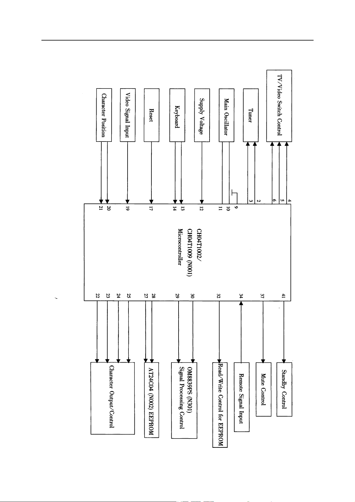
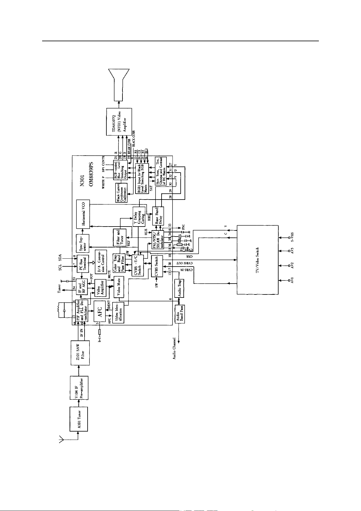
SYSTEM BLOCK DIAGRAMS
Fig.1 Block Diagram for CH-10C1(S) Remote Control Structur
4
Page 7
SERVICE MANUAL
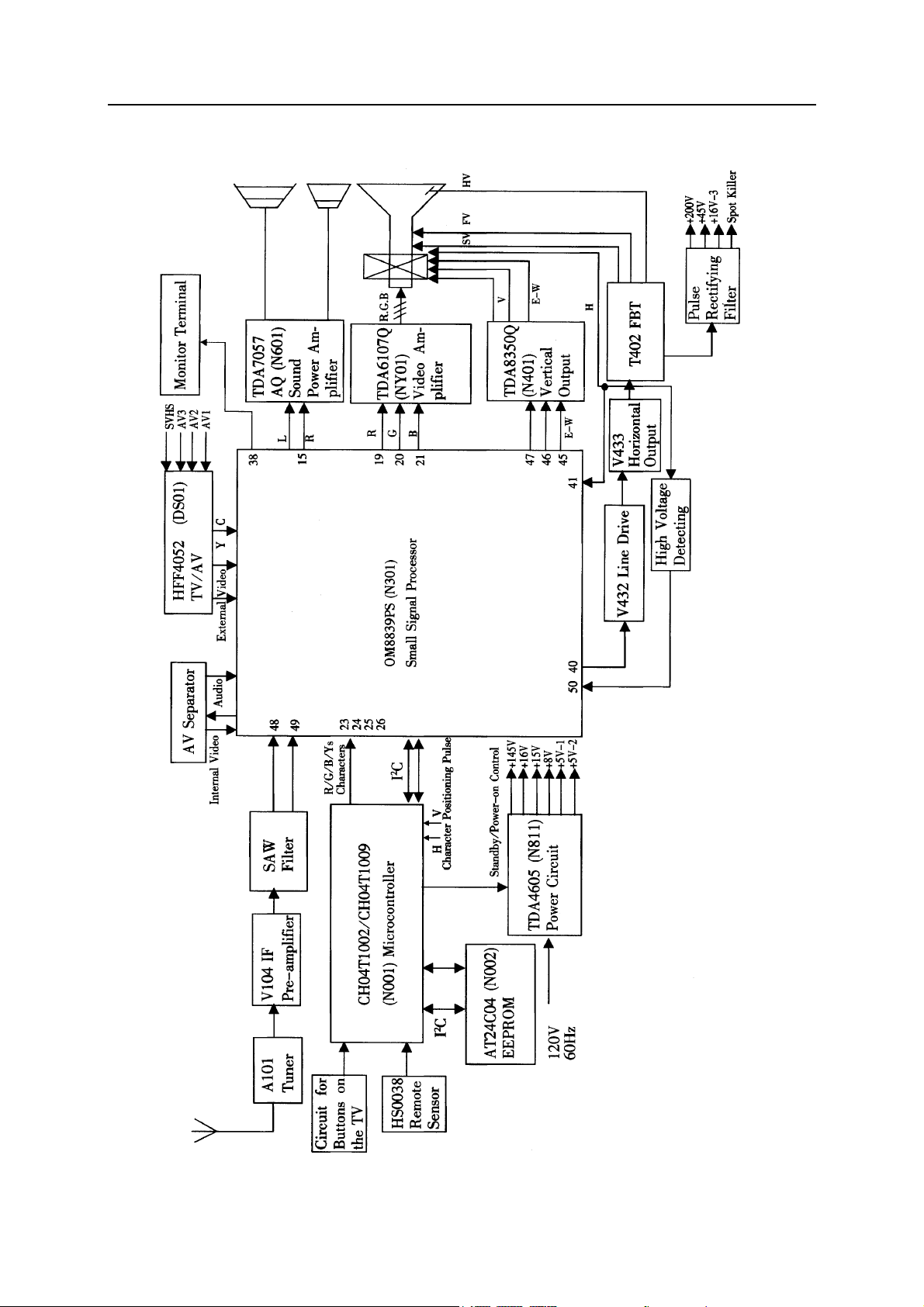
SYSTEM BLOCK DIAGRAMS
(continued)
Fig. 2 Structure Block Diagram for CH-10C1(S) Chassis
5
Page 8
SERVICE MANUAL
SYSTEM BLOCK DIAGRAMS
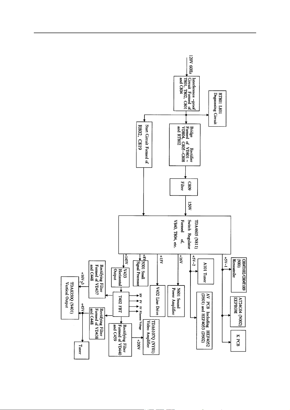
Fig. 3 Block Diagram for CH-10C1(S) Supply Voltage System
(continued)
6
Page 9
SERVICE MANUAL
SYSTEM BLOCK DIAGRAMS
(continued)
Fig. 4 Block Diagram for CH-10C1(S) Video Signal Processor
7
Page 10
SERVICE MANUAL
IC DATA AND WAVEFORMS OF KEY POINTS
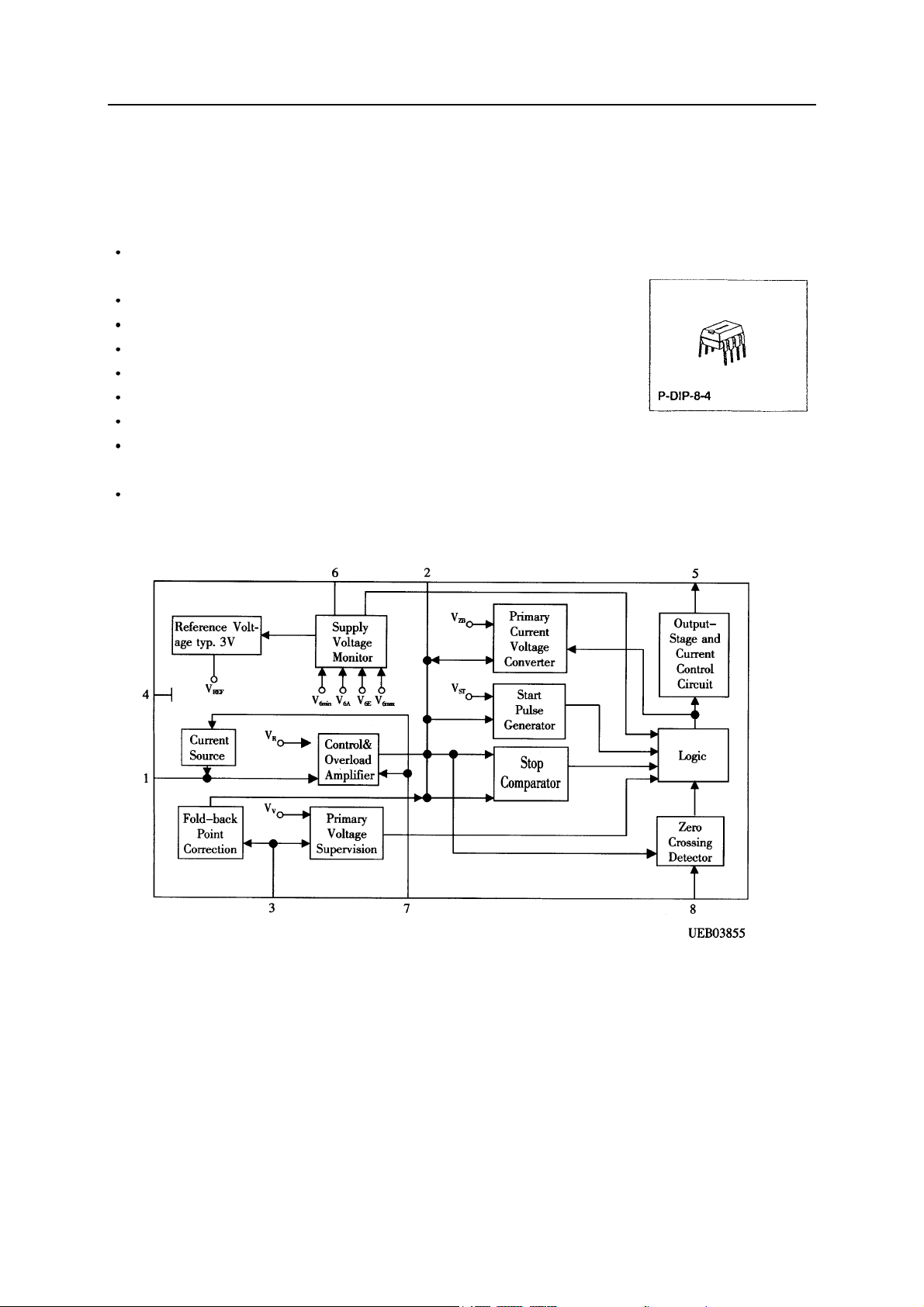
TDA 4605
Control IC for Switched-Mode Power Supplies Using MOS-Transistor
1. Features
Fold-back characterisitics provides overload protection for external
components
Burst operation under secondary short-circuit condition implemented
Protection against open or a short of the control loop
Switch-off if line voltage is too low (undervoltage switch-off)
Line voltage depending compensation of fold-back point
Soft-start for quiet start-up without noise generated by the transformer
Chip-over temperature protection implemented(thermal shutdown)
On-chip ringing suppression circuit against parasitic oscillations of the
transformer
AGC-voltage reduction at low load
2. Block Diagram
Fig. 11
3. Refer to Table 3 about Functions and Data of the IC’s Each Pin.
Fig. 10
8
Page 11
SERVICE MANUAL
IC DATA AND WAVEFORMS OF KEY POINTS (continued)
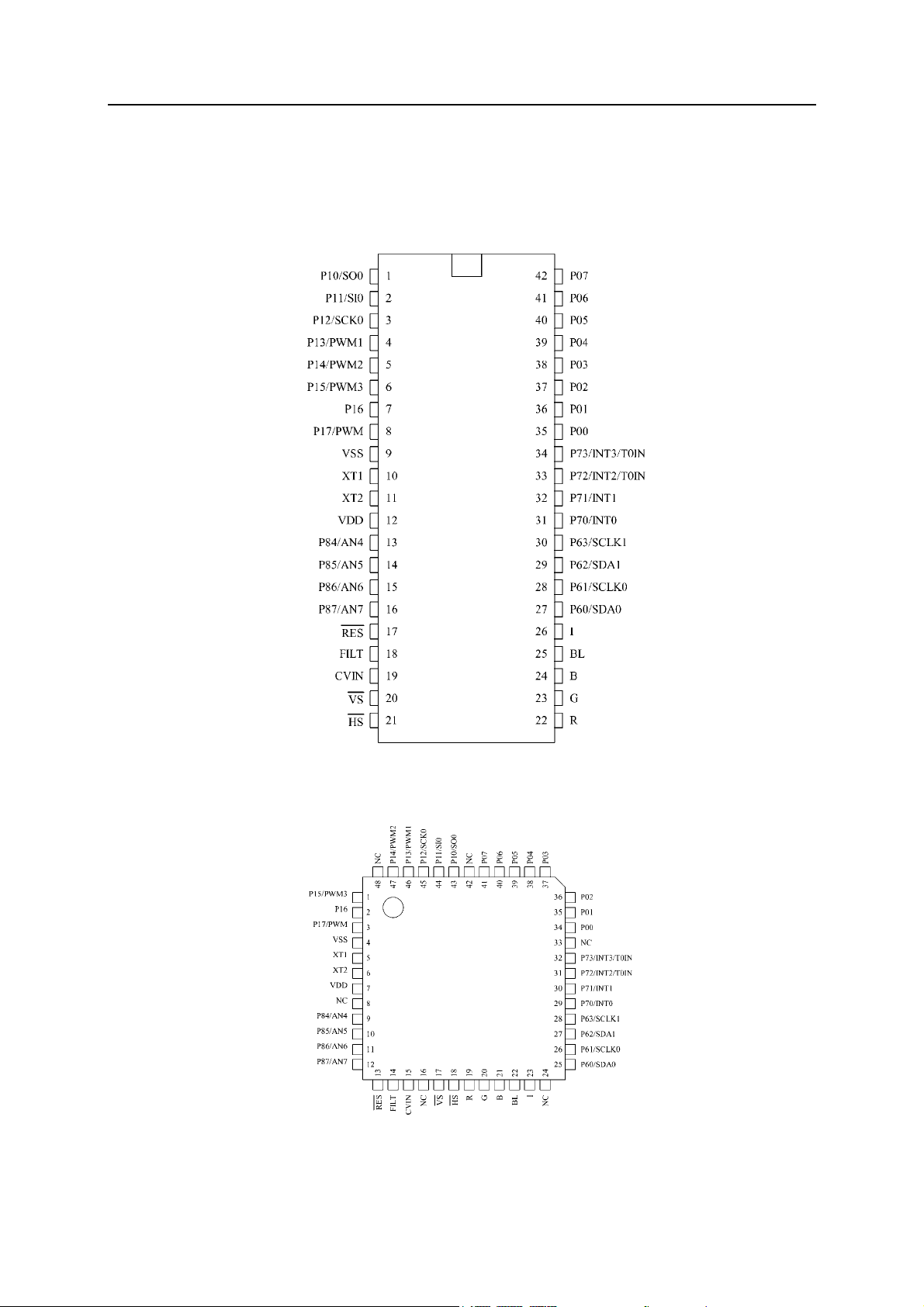
CH04T1002/ CH04T1009
1. Terminal Assignment Layouts
Fig. 12 CH04T1002/ CH04T1009 DIP42S Terminal Assignment Layoutd
Fig. 13 CH04T1002/ CH04T1009 QIP48E Terminal Assignment Layout
9
Page 12
SERVICE MANUAL
IC DATA AND WAVEFORMS OF KEY POINTS (continued)
CH04T1002/ CH04T1009 (continued)
2. Terminal Function
Table 2 Terminal Function Table
Terminal I/O Function Description Option Format
VSS - Negative power supply
XT1 1 Input terminal for crystal oscillation
XT2 O Output terminal for crystal oscillation
VDD - Positive power supply
RES I Reset terminal A
FILT O Charge-pump ouput terminal N
CVIN I
VS I
HS I
R O
G O
B O Blue (B) output terminal of RGB imagee
I O Intensity (I) output terminal of RGB image
BL O
Part 0
P00-p07
Port 1
P10-P17
Port 6
Image signal input terminal
(available only in CH04T1002)
Vertical synchronization signal input terminal
Horizontal synchronization signal input terminal
Red (R) output terminal of RGB image
Green (G) output terminal of RGB image
Fast blanking control signal
Switch TV image and caption/OSD image signal
8-bit input/output port
Input/output can be specified in nibble unit
I/O
I/O
I/O
Other functions:
Hold release input
Internal input
8-bit input/output port
Each bit can be independently
programmable
Other functions:
P10 SIO0 data output
P11 SIO0 data input/bus input/output
P12 SIO0 clock input/output
P13 PWM1 output
P14 PWM2 output
P15 PWM3 output
P17 Timer 1(PWM) output
4-bit input/output port
Each bit can be independently
programmable
Other functions:
P60 IIC0 data input/output
P61 IIC0 clock output
P62 IIC1 data input/output
P63 IIC1 clock output
Pull-up resistor
provided/not
provided
Output format
CMOS/Nch-OD
Output format
CMOS/Nch-OD
M
A
O
E
F
10
Page 13

SERVICE MANUAL
IC DATA AND WAVEFORMS OF KEY POINTS
(continued)
CH04T1002/CH04T1009 (continued)
Terminal I/O Function Description Option Format
P70
W
P71-P73
V
Port 7
P71-P73
I/O
4-bit input/output port
Each bit can be independently
programmable
Other functions:
P70
P71 INT1 input/HOLD release input
P72 INT2 input/timer 0 event input
P73
Interrupt receiver format vector address
INTO
INT1
INT2
INT3
INTO input/HOLD release input
/Nch-Tr. output for watchdog timer
INT3 input (noise rejection filter attached
input)/timer 0 event input
Rising Falling
yes
yes
yes
yes
yes
yes
yes
yes
Rising/
Falling
no
no
yes
yes
H level L level Vector
yes
yes
no
no
yes
yes
no
no
03H
0BH
13H
1BH
Port 8
P83
P84-P87
Port options can be specified independently for each bit.
The programmable pull-up resistors are provided, depending on whether CMOS or Nch-OD (Nch
open drain ) is selected as the port 1 option.
3. Refer to Table 3 about Functions and Data of the IC’s Each Pin.
I/O
1-bit input port
(P83 is set only in CH04T1002)
4-bit input/output port(P84-P87)
I
Each bit can be independently
programmable
Other function:
AD converter input port
P83
B
P84-P87
X
11
Page 14

SERVICE MANUAL
IC DATA AND WAVEFORMS OF KEY POINTS
EEPROM AT24C04
1. Features
Data EEPROM internally organized as 512
bytes and 32 pages×16 bytes
Low power CMOS
Vcc=2.7 to 5.5V operation
Two wire serial interface bus I2C-Bus
compatible
Filtered inputs for noise suppression with
Schmitt trigger
Clock frequency up to 400 kHz
High programming flexibility
-Internal programming voltage
-Self timed programming cycle including erase
-Byte-write and page-write programming
between 1 and 16 bytes
-Typical programming time 6 ms(<10ms) for up
to 16 bytes
High reliability
-Endurance 10
-Data retention 40 years
-ESD protection 4000 V on all pins
8 pin DIP/DSO packages
Available for extended temperature ranges
-Industrial
-Automotive
3. Block Diagram
6
cycles1)
-40 to +85
-40 to +125
1)
2. Pin Configuration
4. Refer to Table 5 about Functions and
Data of the IC’s Each Pin
(continued)
Fig. 14
Fig. 15
12
Page 15

SERVICE MANUAL
IC DATA AND WAVEFORMS OF KEY POINTS
OM8839PS/TDA8843-N2
I2C-bus Controlled PAL/NTSC/SECAM TV Processors
1. Features
The following features are available in all IC
·Multi-standard vision IF circuit with an
alignment-free PLL demodulator without external
components
·Alignment-free multi-standard FM sound
demodulator (4.5 MHz to 6.5 MHz)
·Audio switch
·Flexible source selection with CVBS switch and
Y(CVBS)/C input so that a comb filter can be
applied
·Integrated chrominance trap circuit
·Integrated luminance delay line
·Asymmetrical peaking in the luminance channel
with a (defeatable) noise coring function
·Black stretching of non-standard CVBS or
lumina-nce signals
·Integrated chroma band-pass filter with
switchable centre frequency
·Dynamic skin tone control circuit
·Blue stretch circuit which offsets colours near
white towards blue
·RGB control circuit with “Continuous Cathode
Calibration” and white point adjustment
·Possibility to insert a“blue back” option when no
video signal is available
·Horizontal synchronization with two control loops
and alignment-free horizontal oscillator
·Vertical count-down circuit
·Vertical driver optimised for DC-coupled vertical
output stages
2
C-bus control of various functions
·I
s:
2. General Description
The various versions of the TDA 884X/5X
series are I2C-bus controlled single chip TV
processors which are intended to be applied
in PAL, NTSC, PAL/NTSC and multi-standard
television receivers. The N2 version is pin and
application compatible with the N1 version,
however, a new feature has been added
which makes the N2 more attractive. The IF
PLL demodulator has been replaced by an
alignment-free IF PLL demodulator with
inter-nal VCO (no tuned circuit required). The
setting of the various frequencies (33.4,
33.9,38, 38.9, 45, 75 and 58.75 MHz) can be
made via the I
Because of this difference the N2 version is
compatible with the N1, however, N1 devices
cannot be used in an optimised N2
application.
Functionally the IC series is split up in 3
categories, viz:
·Versions intended to be used in economy TV
receivers with all basic functions (envelope:
S-DIP 56 and QFP 64)
·Versions with additional features like E-W
geometry control, H-V zoom function and
YUV interface which are intended for TV
receivers with 110° picture tubes (envelope:
S-DIP 56)
·Versions which have in addition a second
RGB input with saturation control and a
second CVBS output (envelope: QFP 64)
The various type numbers are given in the
table below.
(continued)
2
C-bus.
3. Survey of IC Types
Envelope S-DIP 56 QFP 64
TV receiver category Economy Mid/High end Economy Mid/High end
PAL only TDA 8840 TDA 8840H
PAL/NTSC TDA 8841 TDA 8843 TDA 8841H
PAL/SECAM/NTSC TDA 8842 TDA 8844 TDA 8842H TDA 8854H
NTSC only TDA 8846/46A TDA 8847 TDA 8857H
13
Page 16

SERVICE MANUAL
IC DATA AND WAVEFORMS OF KEY POINTS
OM8839PS/TDA8843-N2 (continued)
4. Block Diagram
(continued)
Fig .16 Block Diagram “Economy Versions” (S-DIP 56 Envelope)
5. Refer to Table 6 about Functions and Data of the IC’s Each Pin.
14
Page 17

SERVICE MANUAL
IC DATA AND WAVEFORMS OF KEY POINTS
TDA8350Q
DC-coupled Vertical Deflection and East-West
Output Circuit
1. Features
Few extemal components
Highly efficient fully DC-coupled vertical output
bridge circuit
Vertical flyback switch
Guard circuit
Protection against
- short-circuit of the output pins
- short-circuit of the output pins to Vp
3.Block Diagram
High EMC immunity due to common mode
inputs
Temperature (thermal) protection
East-West output stage with one single
conversion resistor.
2. General Description
The TDA8350Q is a power circuit for use in
90° and 110° colour deflection systems for
field frequencies of 50 to 120 Hz. The circuit
provides a DC driven vertical deflection output
circuit, operating as a highly efficient class G
system and an East-West driver for sinking the
diode modulator current.
(continued)
Fig. 17 Block Diagram
4. Refer to Table 7 about Functions and Data of the IC’s Each Pin.
15
Page 18
SERVICE MANUAL
IC DATA AND WAVEFORMS OF KEY POINTS
(continued)
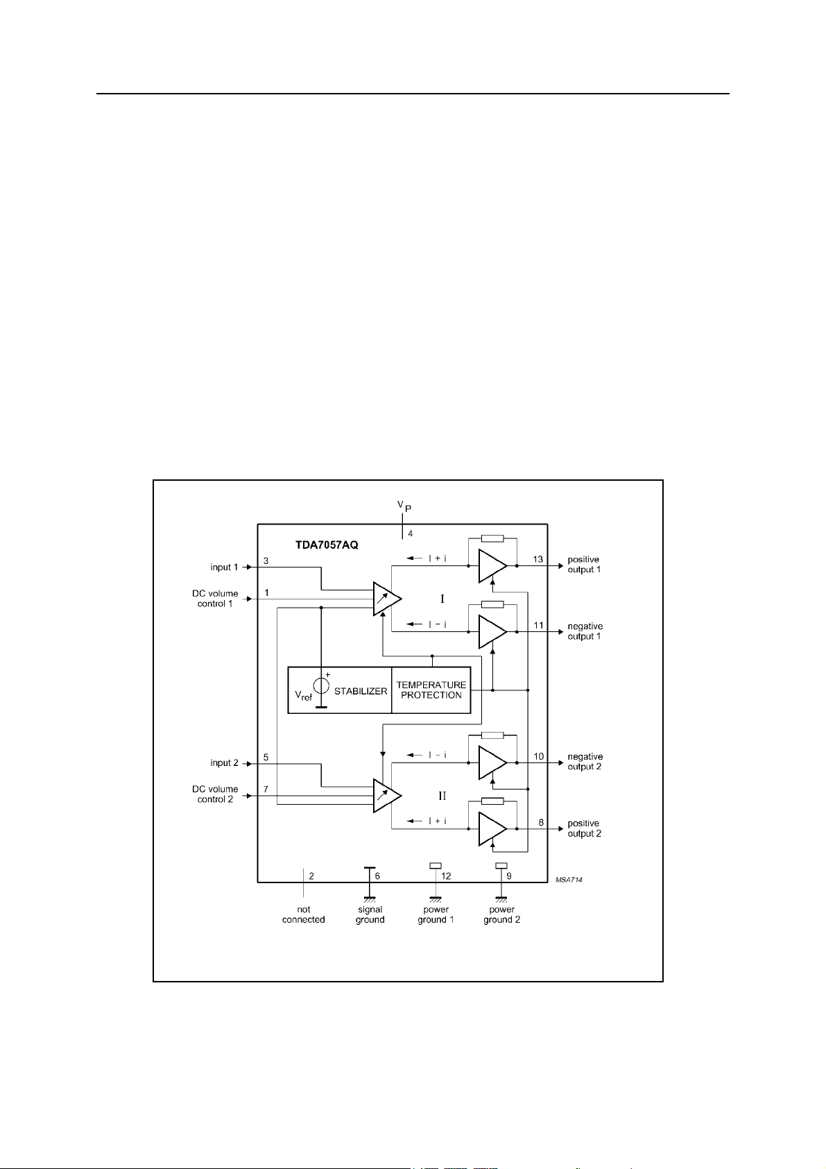
TDA7057AQ
2×8W Stereo BTL Audio Output Amplifier with DC Volume Control
1. Features
·DC volume control
·Few external components
·Mute mode
·Thermal protection
·Short-circuit proof
·No switch-on and switch-off clicks
·Good overall stability
·Low power consumption
·Low HF radiation
·ESD protected on all pins.
3. Block Diagram
General Description
The TDA7057AQ is a stereo BTL output amplifier with DC
volume control. The device is designed for use in TVs and
monitiors, but is also suitable for battery-fed portable
recorders and radios.
issing Current Limiter (MCL)
A MCL protection circuit is built-in. The MCL circuit is
activated when the difference in current between the output
terminal of each amplifier exceeds 100 mA (typical 300
mA). This level of 100 mA allows for single-ended
headphone applications.
Fig. 18 Block Diagram
4. Refer to Table 8 about Functions and Data of the IC’s Each Pin.
16
Page 19
SERVICE MANUAL
IC DATA AND WAVEFORMS OF KEY POINTS
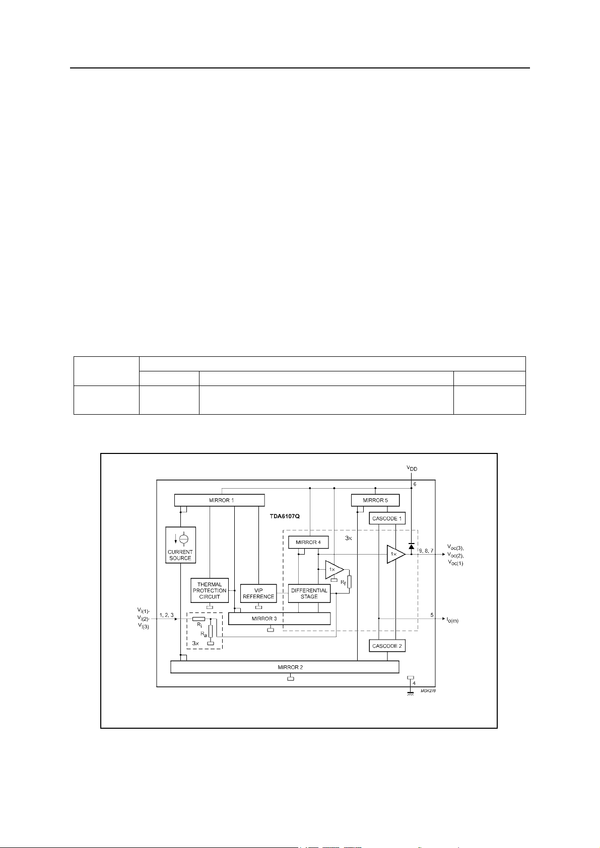
TDA6107Q
Triple Video Output Amplifier
1. Features
·Typical bandwidth of 5.5 MHz for an output
signal of 60 V (p-p)
·High slew rate of 900 V/S
·No external components required
·Very simple application
·Single supply voltage of 200 V
·Internal reference voltage of 2.5 V
·Fixed gain of 50
·Black-Current Stabilization (BCS) circuit
·Thermal protection.
3. Ordering Information
Type
Number
TDA6107Q DBS9MPF
Name Description Version
Plastic DIL-bent-SIL medium power package with fin; 9
leads
2. General Description
The TDA6107Q includes three video output
amplifiers in one plastic DIL-bent-SIL 9-pin
medium power (DBS9MPF) package (SOT
111-1), using high-voltage DMOS technology,
and is intended to drive the three cathodes of a
colour CRT directly. To obtain maximum
performance, the amplifier should be used with
black-current control.
Package
(continued)
SOT 111 - 1
4. Block Diagram
Fig. 19 Block Diagram (One Amplifier Shown)
5. Refer to Table 9 about Functions and Data of the IC’s Each Pin.
17
Page 20

SERVICE MANUAL
o
IC DATA AND WAVEFORMS OF KEY POINTS
HEF4052
Dual 4-channel Analog Multiplexer/Demultiplexer
E
1. Description
The HEF4052 is a dual 4-channel analog
multiplexer/demultiplexer with common
channel select logic. Each
multiplexer/demultiplexer has four independent
inputs/outputs (Y
input/output (Z). The common channel select
logic includes two address inputs (A
to Y3) and a common
0
0
and A1)
and an active LOW enable input (E).
Both multiplexers/demultiplexers contain four
bidirectional analog switches, each with one
side connected to an independent input/output
(Y
to Y3) and the other side connected to a
0
common input/output(Z).
2. Block Diagrams
Fig. 20 Functional Diagram
With
(low impedance ON-state) by A
HIGH, all switches are in the high impedance
OFF-state, independent of A0 and A1. VDD and Vss
are the supply voltage connections for the digital
control inputs (A0, A1 and E). The VDD to Vss
range is 3 to 15 V. The analog inputs/outputs (Y
Y3, and Z) can swing between VDD as a positive
limit and VEE as a negative limit.
V
For operation as a digital multiplexer/
demultiplexer, VEE is connected to VSS (typically
ground).
LOW, one of the four switches is selected
may not exceed 15 V.
DD-VEE
Pinning
to Y3A Independent inputs/outputs
Y
OA
Y
to Y3B Independent inputs/outputs
OB
A
A1 Address inputs
O
E
Enable input (active LOW)
Z
ZB Common inputs/outputs
A
Family data,
lDD LIMITS category MSI
See Family Specifications
HEF4052P (N): 16-lead DIL; plastic
(SOT38-1)
HEF4052D (F) 16-lead DIL; ceramic
(cerdip)
(SOT74)
HEF4052T (D): 16-lead SO; plastic
(SOT109-1)
(): Package Designator North America
(continued)
and A1. With E
0
Fig. 21 Pinning Diagram
t
0
18
Page 21

SERVICE MANUAL
IC DATA AND WAVEFORMS OF KEY POINTS
(continued)
HEF4052 (continued)
Fig. 22 Schematic Diagram (One Switch)
3. Function Table
Inputs Channel
E
L L L Y
L L H Y
L H L Y
L H H Y
H X X none
Notes
H=HIGH state (the more positive voltage)
L=LOW state (the less positive voltage)
X=state is immaterial
Ratings
Limiting values in accordance with the Absolute Maximum System (IEC 134)
Supply voltage (with reference to V
Note
To avoid drawing V
drop across the bidirectional switch must not exceed 0,4V. If the switch current flows into terminal Z,
no V
DD
but the voltages at Y and Z may not exceed V
4. Refer to Table 10 about Functions and Data of the IC
A1 A0 On
; YOB-ZB
OA-ZA
; Y1B-ZB
1A-ZA
; Y2B-ZB
2A-ZA
; Y3B-ZB
3A-ZA
) VEE -18 to +0,5 V
DD
current out of terminal Z, when switch current flows into terminals Y, the voltage
DD
current will flow out of terminals Y, in this case is no limit for the voltage drop across the switch,
or VEE
DD
s Each Pin.
19
Page 22

SERVICE MANUAL
IC DATA AND WAVEFORMS OF KEY POINTS
HEF4053
Triple 2-channel Analog
Multiplexer/Demultiplexer
1. Description
The HEF4053 is a triple 2-channel analog
multiplexer/demultiplexer with a common enable
E
input (
). Each multiplexer/demultiplexer has
two indepen-
dent inputs/outputs (Y
and Y1), a common
0
input/output (Z), and select inputs (Sn). Each
also contains two-bidirectional analog switches,
each with one side connected to an independent
input/output (Y
and Y1) and the other side
0
connected to a common input/output (Z).
E
With (
d to V
) LOW, one of the two switches is
(typically ground)
SS
2. Block Diagrams
Fig.23 Functional Diagram
selected
(low impedance ON-state) by Sn. With
HIGH, all switches are in the high impedance
OFF-state, independent of S
V
and VSS are the supply voltage connections
DD
for the digital control inputs (S
The V
inputs/outputs (Y
V
V
to VSS range is 3 to 15V.The analog
DD
0
as a positive limit and VEE as a negative limit.
DD
may not exceed 15 V.
DD-VEE
For operation as a digital
multiplexer/demultiplexer, V
(continued)
E
to SC.
A
to SC and E).
A
, Y1 and Z) can swing between
is connecte
EE
20
Page 23

SERVICE MANUAL
IC DATA AND WAVEFORMS OF KEY POINTS (continued)
HEF4053
HEF4053P(N): 16-lead DIL; plastic
HEF4053D(F): 16-lead DIL; ceramic
HEF4053T(D): 16-lead S0; plastic
( ): Package Designator North America
(continued)
Fig. 20 Pinning Diagram
(SOT38-1)
(cerdip)
(SOT74)
(SOT109-1)
Pinning
to Y0C
Y
0A
Y
1A to Y1C
S
A
Independent inputs/outputs
to Sc Select inputs
Independent inputs/outputs
E Enable input (active LOW)
to ZC Common inputs/outputs
Z
A
3. Function Table
Inputs Channel
E Sn On
L L Y
L H Y1n-Zn
X none
H
Notes
H=HIGH state (the more positive voltage)
L=LOW state (the less positive voltage)
X=STATE is immaterial
n-Zn
0
Fig. 25 Schematic Diagram (One Switch)
Ratings
Limiting values in accordance with the Absolute Maximum System (IEC 134)
Supply voltage (with reference to V
) VEE -18 to + 0,5 V
DD
Note
To avoid drawing V
current out of terminal Z, when switch current flows into terminals Y, the voltage
DD
drop across the bidirecctional switch must not exceed 0, 4 V. If the switch current flows into terminal
Z, no V
the switch, but the voltages at Y and Z may not exceed V
4. Refer to Table 11 about Functions and Data of the IC
current will flow out of terminals Y, in this case there is no limit for the voltage drop across
DD
DD
or V
EE.
s Each Pin.
21
Page 24

SERVICE MANUAL
IC DATA AND WAVEFORMS OF KEY POINTS (continued)
Table 3 Functions and Service Data of TDA4605 (N811)’s Pins
Pin No. Function Description
1 Regulation control 0.4 0.713 0.4
2 Primary current input 1.34 9.71 1.34
3 Primary voltage monitoring input 1.91 7.09 1.91
4 Groundy 0 0 0
5 Drive pulse output 4.08 0.84 4.08
6 Supply voltage 0.74 16.35 4.9
7 Soft-start 2.36 8.69 6.19
8 Zero crossing input detection 0.33 6.72 5.94
Reference Voltage (V) Positive Resistance (KΩ) Negative Resistance (KΩ)
Digital Multimeter
Table 4 Functions and Service Data of CH04T1009 (N001)’s Pins
. Function Description
Pin No
1 Not connected 0 9.62 5.35
2 Clock line 4.89 9.56 5.08
3 Data line 4.87 9.56 5.06
4 AV1 control 5 6.84 5.22
5 AV2 control 0 6.89 5.16
6 AV3 control 0 7.28 5.29
7 Not connected 0 9.61 5.4
8 Not connected 0.92 9.6 5.4
9 Ground 0 0 0
10 Input terminal for clock oscillating signal 1.88 9.55 6.12
11 Output termin
12 Power supply 5 3.64 3.33
13 Button-control voltage input terminal 5 8.91 5.21
14 Button-control voltage input terminal 5 8.93 5.21
15 Not connected 5 9.45 5.45
16 Not connected 4.9 9.53 5.45
17 Reset 4.96 4.64 4.48
18 Filter 2.76 9.52 5.31
19 Video signal input terminal 3 9.51 5.92
20 Input terminal for vertical flyback pulse 4.74 8.73 5.03
21 Input terminal for horizontal flyback pulse 4.27 8.81 5.01
22 R character output terminal 0 2.08 2.08
23 G character output terminal 0 2.1 2.1
24 B character output terminal 0 2.08 2.08
25 Output terminal for fast blanking signal 0 1.97 1.97
26 Character level clamping 0 9.54 5.73
27 Clock line 0 5 7.12 4.91
28 Data line0 5 7.12 5.18
29 Clock line 1 4.52 7.05 5.12
al for clock oscillating signal
Reference Voltage (V) Positive Resistance (KΩ) Negative Resistance (KΩ)
2.63 9.05 6.08
Digital Multimeter
(continued)
22
Page 25
SERVICE MANUAL
IC DATA AND WAVEFORMS OF KEY POINTS (continued)
30 Data line 1 4.41 7.03 5.09
31 Overload detecting input terminal 5 6.95 5.13
Input terminal for selectable production
32
modes
33 Not connected 0 9.56 5.46
34 Remote control input 4.64 9.22 5.33
35 Not connected 0 9.58 5.4
36 Not connected 0 9.58 5.42
37 Mute 0 9.58 4.3
38 Not connected 0 9.58 5.36
39 Not connected 0 9.59 5.28
40 Not connected 0 9.59 5.36
41 Standby control 0 7.43 4.9
42 Not connected 0 9.6 5.36
5 9.62 5.29
Table 5 Functions and Service Data of AT24C04 (N002)’s Pins
Pin No. Function Description
1 Address input 0 0 0
2 Address input 0 0 0
3 Address input 0 0 0
4 Common ground 0 0 0
5 Clock line 5 7.05 4.82
6 Data line 5 7.06 5.24
7 Write protect 4.99 9.58 5.49
8 Power supply 5 3.64 3.33
Reference Voltage (V) Positive Resistance (KΩ) Negative Resistance (KΩ)
Digital Multimeter
Table 6 Functions and Service Data of OM8839PS (N301)’s Pins
Pin No. Function Description
1 SIF signal input 0 2.21 2.21
External audio signal input
2
Reference frequency resonant coil terminal
3
Reference frequency resonant coil terminal
4
PLL filter
5
Video detection output
6
Clock line
7
Two-way transmission data line
8
Gap decoupling
9
SVHS chroma signal input
10
SVHS luminance signal input
11
Supply voltage
12
Composite video signal input terminal
13
Ground
14
Reference Voltage (V) Positive Resistance (KΩ) Negative Resistance (KΩ)
3.65 9.02 6.04
0
0
2.51 8.92 5.82
3.06 2.2 2.2
4.4 7.15 5.15
4.52 7.15 5.15
6.7 7.52 5.68
1.35 9 6
3.4 9.04 5.91
8.24 2.78 1.96
4.32 9.15 5.94
0 0 0
Digital Multimeter
(continued)
23
Page 26

SERVICE MANUAL
IC DATA AND WAVEFORMS OF KEY POINTS (continued)
15 Audio signal output 3 9.24 5.98
16 Decoupling capacitor connection 0
17 Video input 3.4 9.12 5.94
18 Black current control input 5.81 9.22 5.88
19 Blue (B) signal output 3.04 6.19 5.2
20 Green (G) signal output 3.1 6.19 5.23
21 Red (R) signal output 3.2 6.2 5.26
22 Beam current control 2.1 8.22 6.04
23 Red (R) signal input 3.6 9.01 6.12
24 Green (G) signal input 3.61 9.01 6.12
25 Blue (B) signal input 3.6 9.01 6.12
Selectable primary color signal input
26
control
27 Luminance signal input 3.26 9.25 5.87
28 Luminance signal output 3.26 9.25 5.87
29 B-Y color difference signal output 2.38 8.5 5.91
30 R-Y color difference signal output 2.37 8.5 5.91
31 B-Y color difference signal input 2.38 8.5 5.91
32 R-Y color difference signal input 2.37 8.5 5.91
Sub-carrier output for SECAM
33
demodulation
34 3.58MHz crystal oscillator 2.54 8.02 6.04
35 4.43MHz crystal oscillator 2.53 8.02 6.04
36 APC low pass filter 4.99 9.37 6
37 Horizontal starting supply voltage 8.22 2.64 2.56
38 Composite video output 3.68 7.52 6.11
39 Black level stretch 4.95 9.26 4.93
40 Line drive pulse output 3.55 3.5 3.49
Horizontal flyback pulse input /
41
sandcastle pulse output
42 Line discriminator 3.66 8.81 6.04
43 Line discriminator 3.92 9.31 6.04
44 Ground 0 0 0
45 Vertical frequency parabola output 0.73 9.05 5.97
46 Field drive signal output 2.32 9.3 5.97
47 Field drive signal output 2.35 9.3 5.97
48 IF signal input 4.62 8.52 6.2
49 IF signal input 4.62 8.52 6.2
50 High voltage detection input 2.05 8.04 6.14
51 Vertical sawtooth generation 3.8 8.65 6.09
52 Vertical reference bias setting 3.9 8.89 6.05
53 AGC filter for IF amplifier 4.49 9.25 6
54 AGC output for IF amplifier 0.67 10.05 5.82
55 Audio deemphasis 2.93 8.93 6.12
56 Audio decoupling
0.1 1 1
0.35 6.78 5.96
0.76 8.82 5.92
4.02 9.37 6.08
24
Page 27

SERVICE MANUAL
IC DATA AND WAVEFORMS OF KEY POINTS (continued)
Table 7 Functions and Service Data of TDA8350 (N401)’s Pins
Pin No. Function Description
1 Vertical drive input (positive) 2.32 9.4 5.84
2 Vertical drive input (negative) 2.3 9.4 5.87
3 Feedback input 8.15 5.81 4.72
4 Supply voltage 16.27 7.99 7.62
5 Output 1 8.14 5.88 4.72
6 Not connected 0
7 Ground 0 0 0
8 Pump supply voltage input 46.94 4.29
9 Output 1 8.22 5.92 4.71
10 Guard output 0.28 8.51 5.899
11 Pincushion output 16.99 9.45 4.16
12 Pincushion input (negative) 0.25 9.12 5.93
13 Pincushion input (positive) 0 0 0
Reference Voltage (V) Positive Resistance (KΩ) Negative Resistance (KΩ)
Digital Multimeter
Table 8 Functions and Service Data of TDA7057AQ (N601)’s Pins
Pin No. Function Description
1 Volume control input 1.03 6.88 6.15
2 Not connected 0
3 Audio R signal input 2.45 12.68 6.5
4 Supply voltage 16.18 0.46 0.46
5 Audio L signal input 2.45 12.6 6.5
6 Ground 0 0 0
7 Volume control input 1.03 6.88 6.15
8 Left channel in-phase signal output 7.64 6.48 5.6
9 Ground 0 0 0
10 Left channel inverting signal output 7.71 6.47 5.6
11 Right channel inverting signal output 7.67 6.47 5.6
12 Ground 0 0 0
13 Right channel in-phase signal output 7.79 6.48 5.6
Reference Voltage (V) Positive Resistance (KΩ) Negative Resistance (KΩ)
Digital Multimeter
Table 9 Functions and Service Data of TDA6017Q’s Pins
Pin No. Function Description
1 G inverting input 2.94 5.72 4.96
2 R inverting input 3 5.72 4.96
3 B inverting input 2.91 5.72 4.96
4 Ground 0 0 0
5 Black level current input 6.5 19.28 5.68
6 Supply voltage 198.65 4.53
7 B output 103 5.48
8 R output 98.6 5.48
9 G output 100.6 5.48
Reference Voltage (V) Positive Resistance (KΩ) Negative Resistance (KΩ)
Digital Multimeter
25
Page 28
SERVICE MANUAL
IC DATA AND WAVEFORMS OF KEY POINTS (continued)
Table 10 Functions and Service Data of HEF4052 (DS01)’s Pins
Pin No. Function Description
1 Switch input 0.3 7.5 26
2 Switch input 0 7.5 26
3 Switch output 0 2.3 2.3
4 Switch input 0.4 7.5 26
5 Switch input 0 7.5 26
6 Inhibit terminal 0 0 0
7 VEE 0 0 0
8 Ground 0 0 0
9 Control signal input 3.5 10 6.3
10 Control signal input 3.5 10 6.3
11 Switch input 3 0.5 0.5
12 Switch input 3 0.5 0.5
13 Switch output 3.5 2.3 2.3
14 Switch input 2.8 0.5 0.5
15 Switch input 3 0.5 0.5
16 Supply voltage 7.8 1.5 1.5
Reference Voltage (V) Positive Resistance (KΩ) Negative Resistance (KΩ)
Digital Multimeter
Table 11 Functions and Service Data of HEF4053 (DS02)’s Pins
Pin No. Function Description
1 Signal input 0 9.81 6.15
2 Signal input 0 0 0
3 Signal input 0 9.81 6.15
4 Signal output 0 6.66 6.21
5 Signal input 0 0 0
6 Ground 0 0 0
7 Ground 0 0 0
8 Ground 0 0 0
9 Control signal input 0.12 7.97 5.7
10 Control signal input 0.12 7.99 5.7
11 Control signal input 4.98 7.8 5.6
12 Signal input 0 0 0
13 0 9.81 6.15
Signal output
14 Signal input 0 6.9 6.4
15 Audio output 0 6.95 6.4
16 Supply voltage 5.09 6.89 4.44
Reference Voltage (V) Positive Resistance (KΩ) Negative Resistance (KΩ)
Digital Multimeter
Table 12 Functions and Service Data of TDQ-6F2M’s Pinss Pins
Pin No. Function Description
1 AGC 0.98 9.56 6.04
2 NC 26.73 6.85
3 NC 0.61 9.76 7.39
4 SCL 4.89 9.58 5.13
5 SDA 4.88 9.58 5.12
6 VDD 5 2.2 2.2
7 NC 4.9 2.2 2.2
8 NC 0 0 0
9 BT 3.021 13.07
10 NC 0 0 0
11 IF 0
Reference Voltage (V) Positive Resistance (KΩ) Negative Resistance (KΩ)
Digital Multimeter
26
Page 29

SERVICE MANUAL
IC DATA AND WAVEFORMS OF KEY POINTS
(continued)
Note
:
The TV receives NTSC color bar with 1KHz sine wave audio reception in Normal mode when
measuring voltage and resistance with a GDM-8145 multimeter (Max. resistance: 20 KΩ, Max. DC
voltage: 20V).
27
Page 30
SERVICE MANUAL
IC DATA AND WAVEFORMS OF KEY POINTS
(continued)
28
Page 31

SERVICE MANUAL
IC DATA AND WAVEFORMS OF KEY POINTS
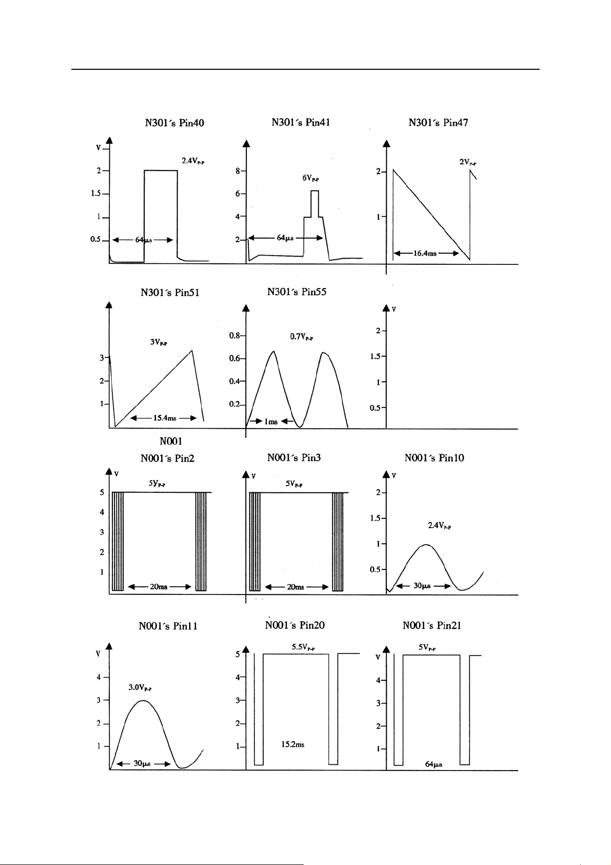
(continued)
Measure with a GOS-622G oscilloscope.
29
Page 32

SERVICE MANUAL
IC DATA AND WAVEFORMS OF KEY POINTS
(continued)
30
Page 33
SERVICE MANUAL
IC DATA AND WAVEFORMS OF KEY POINTS
Serial No. Type
V104 C388A 2.12 8.35 1.35
V609 C1815 2.99 8.47 2.29
V601S C1815 2.54 6.94 1.88
V602S C1815 6.94 8.48 6.24
V204 C1815 2.07 5.08 1.37
V227 C1815 3.66 8.43 2.99
V432 BSN274 2.35 10.70 0
V433 BV2720DF -0.07 113.6 0
V436 A1015 1.67 0 1.98
V437 A1015 8.53 2.05 8.53
V438 C1815 0 8.52 0
V001 C1815 0.06 4.73 0
V002 C1815 0.12 4.28 0
V009 A1015 4.33 4.96 5
V631A C1815 0.19 1.03 0
V632A A1015 8.52 -0.10 8.41
V289 C1815 0.18 7.41 0
V862 C1815 0.18 7.37 0
V863 C3852 0.18 5.17 0
V840 BVZ334 3.92 156.90 0
VS10 C1815 2.40 5.13 1.78
VS20 C1815 2.40 5.13 1.78
VS30 C1815 2.98 5.13 2.32
V217 C1815 0.35 8.53 0
Base
(B)
Collector
(C)
Emitter
(E)
Serial No. Type Input Reference Output
N861 LM317 11.56 7.37 8.63
N863 L7805 15.65 0 5.00
N851 C3852
N402 LM317 15.64 7.41 8.66
+B voltage: 134.49V
AV voltage: 16.23V
Frame supply voltage: 16.73V
(continued)
(B)
5.74
(C)
11.56
(E)
5.17
CIRCUIT ADJUSTMENTS
1. General Description
All adjustments are thoroughly checked and corrected before the TV outgoing. Therefore the TV should
operate normally and deliver proper colour pictures upon installation. However, several minor
adjustments may be required depending on the particular location where the TV is operated.
This TV is shipped completely in carton. Carefully take out the TV from the carton and remove all
packing materials. Connect the power cord into a 120V AC, 60Hz two-pin power outlet. Turn on the TV.
Check and adjust all the customer controls such as brightness, contrast and colour to obtain natural
colour pictures.
2. Automatic Degaussing
31
Page 34

SERVICE MANUAL
A degaussing coil is mounted around the CRT so that external degaussing after moving the TV is
generally unnecessary, providing it is properly degaussed upon installation. The degaussing coil
operates in about 1 second after power on. If the set is moved or faced to a different direction, the
power switch must be switched off for at least 30 minutes in order that the automatic degaussing circuit
operates properly. Should the chassis or parts of the cabinet become magnetized to cause poor colour
purity, use an external-degaussing coil. Slowly move the degaussing coil around the screen the sides
and front of the TV and slowly withdraw the coil to a distance of about 2m before unplug it. If colour
shading still exists, perform the Colour Purity Adjustment and Convergence Adjustment procedures.
3. Supply Voltage Adjustment
Caution: +B voltage has close relation to high voltage. To avoid X-ray radiation +B voltage should
be +145V.
1) Set RV801 to the mechanical center and AC power supply to 120±2V.
2) Connect a digital voltmeter to two pins of C898, and then turn on the TV.
3) Receive Philips test pattern signals.
4) Adjust RN823 to make the voltmeter read 145±0.5V.
4. High Voltage Inspection
Caution: No high voltage adjustment should be done in the chassis.
1) Connect a precise high voltmeter to the second anode of the CRT.
20 Turn on the TV and set the brightness and contrast to minimum (i.e. set beam current of the CRT to
zero).
3) The high voltage tested should be 27.5±0.5KV.
4) Set the brightness to minimum or maximum, and ensure high voltage not beyond limitation of 30KV
in any case.
5. Focus Adjustment
1) Use the remote control to set the contrast to maximum and the brightness, chroma to medium.
2) Set H. V. lines near Philips pattern center to thinnest with the FCB on the FBT. After finishing
adjustment, ensure that no poor focusing exists near the center or around of the frame.
Before Adjusting After Adjusting
32
Page 35
SERVICE MANUAL
g
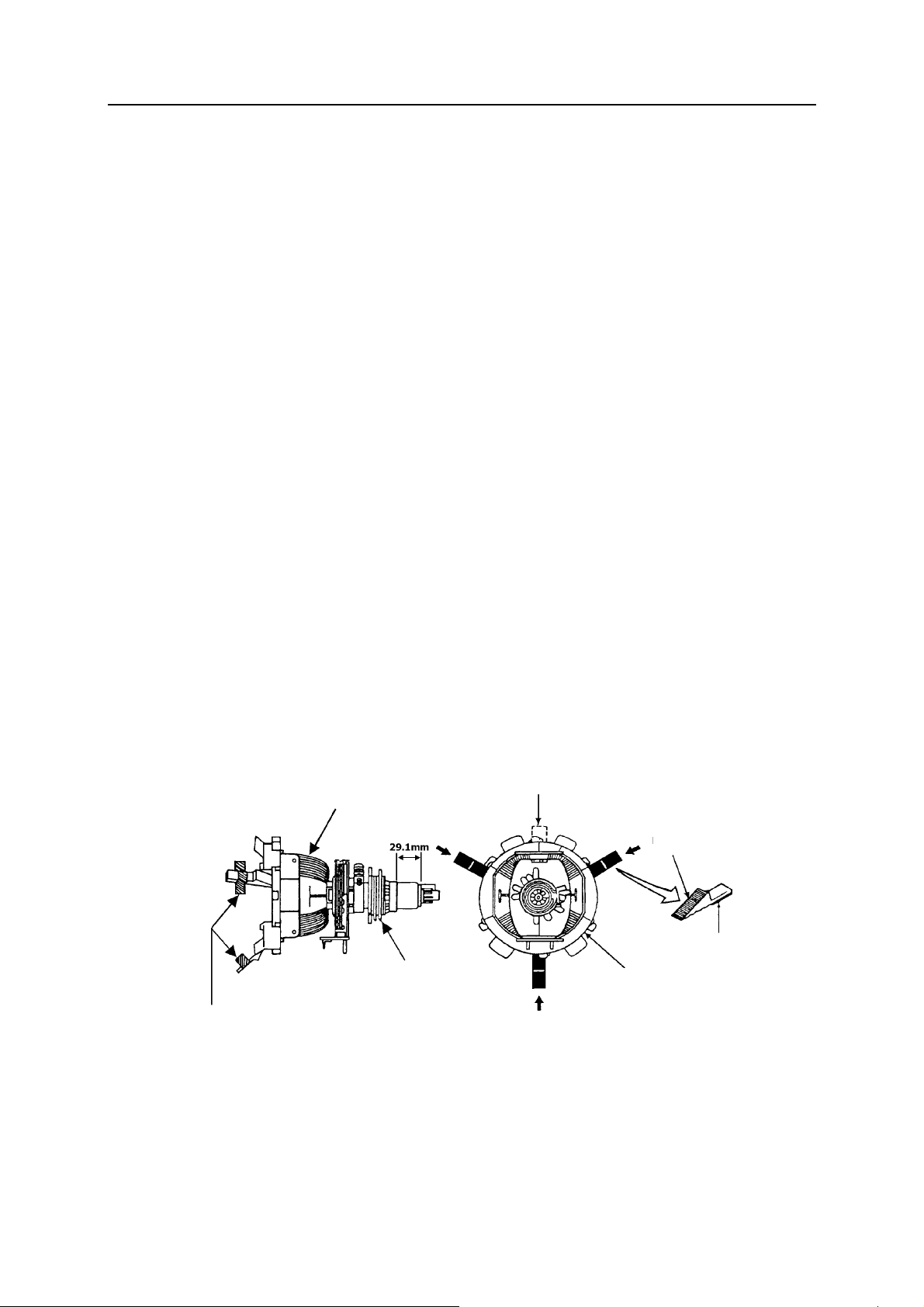
SET-UP ADJUSTMENTS
● The following adjustments should be made when a complete realignment is required or a new CRT is
installed. Perform the adjustments in order as follows.
1. Colour purity
2. Convergence
3. White Balance
Note:
The purity/convergence magnet assembly and rubber wedges need mechanical positioning. Refer to
Fig. 26.
1. Colour Purity Adjustment
Note:
Before attempting any purity adjustment, the TV should be operated for at least 15 minutes.
1) Demagnetize the CRT and cabinet using a degaussing coil.
2) Set the brightness and contrast to maximum.
3) Receive the green raster test signals.
4) Loosen the clamp screw holding the deflection yoke and slide it backward or forward to display
vertical green belt (zone) on the screen.
5) Remove the rubber wedge.
6) Rotate and spread the tabs of the purity magnet around the neck of the CRT until the green belt is on
the centre of the screen.
7) Slowly move the deflection yoke forward or backward until a uniform green screen is obtained.
Tighten the clamp screw of the yoke temporarily.
8) Check purity of the red and blue raster.
Glass Cloth Tapes
Deflection Coil
Purity/Convergence
Ma
net Module
Dummy Wedge
Fig. 26
Rubber Wedge
Adhesive
Deflection Yoke
33
Page 36

SERVICE MANUAL
Adj
(
g
y
SET-UP ADJUSTMENTS (continued) SET-UP ADJUSTMENTS (continued)
6-pole Magnet
4-pole Magnet
Purity Magnet
Conver
2. Convergence Adjustment 2. Convergence Adjustment
Note: Note:
Before attempting any convergence adjustment, the TV should be operated for at least 15 minutes. Before attempting any convergence adjustment, the TV should be operated for at least 15 minutes.
● Center convergence adjustment ● Center convergence adjustment
1) Receive the grille test pattern signals. 1) Receive the grille test pattern signals.
2) Set the brightness and contrast properly. 2) Set the brightness and contrast properly.
3) Adjust two tabs of the 4-pole magnet to change the angle between them and red and blue vertical
3) Adjust two tabs of the 4-pole magnet to change the angle between them and red and blue vertical
lines are superimposed on the center area of the screen.
lines are superimposed on the center area of the screen.
4) Turn both tabs at the same time keeping the angle constant to superimpose red and blue horizontal
4) Turn both tabs at the same time keeping the angle constant to superimpose red and blue horizontal
lines on the center of the screen.
lines on the center of the screen.
5) Adjust two tabs of 6-pole magnet to superimpose red/blue line and green line. Adjusting the angle
5) Adjust two tabs of 6-pole magnet to superimpose red/blue line and green line. Adjusting the angle
affects the vertical lines and rotating both magnets affects the horizontal lines.
affects the vertical lines and rotating both magnets affects the horizontal lines.
6) Repeat steps 3)6) Repeat steps 3)
magnet interact each other, resulting in complicating and dot movement.
● Circumference convergence adjustment
1) Loosen the clamping screw of the defection yoke slightly to allow it to tilt.
2) Temporarily put a wedge as shown in Fig.26. (Do not remove cover paper on adhesive part of the
wedge.)
3) Tilt front of the deflection yoke up or down to obtain better convergence in circumference.
Push the mounted wedge into the space between the CRT and yoke to fix the yoke temporarily.
4) Put other wedge into bottom space and remove the cover paper to stick.
5) Tilt front of the deflection yoke right or left to obtain better convergence in circumference.
6) Keep the deflection yoke position and put another wedge in either upper space. Remove cover
paper and stick the wedge on the CRT to fix the yoke.
7) Detach the temporarily mounted wedge and put it in another upper space. Stick it on the CRT to fix
the yoke.
8) After fixing three wedges, recheck overall convergence.
Tighten the screw firmly to fix the yoke and check if the yoke is fixed.
ence Magnet Assembl
5) keeping in mind red, green and blue movement. 4-pole magnet and 6-pole
ust the Angle (Vertical Lines)
Adjustment of Magnets
Fig. 27
Fig. 27
Rotate Two Tabs At the
Same Time
Fixed
Horizontal Lines)
34
Page 37

SERVICE MANUAL
SET-UP ADJUSTMENTS (continued)
9) Stick three adhesive tapes on wedges as shown in Fig. 26.
BLU
Red
4-pole Magnet Movement 6-pole Magnet Movement
Incline the Yoke up (or down) Incline the Yoke Right(or left)
BLU Red Red/BLU GRN
Red/BLU
GRN
Center Convergence by Convergence Magnets
Circumference Convergence by DEF Yoke
Fig. 28
SERVICE MODE AND BUS DATA
Decrease the volume to 00. Press the MUTE button on the remote control and “Mute”appears on the
TV screen. Then press and hold the MUTE button on the remote control and MENU on the TV at the
same time for 3 seconds and the TV enters the S mode.
Description Data Description Data Description Data Description Data Description Data
AFW:240KHz 1 De interta 0 S CORRECT 20 AUTO ADJUST 0 OPT SPKON 0
IF-PLL 1 H shift 40 V SHIFT 32 SUB BRIGHT 27 OPT SPATAL 1
AGC over f 9 H shift-50 32 V SHIFT-50 32 LOUDNESS 18 OPT COLOR 0
IFS 0 E/W WIDE 45 V 200M 25 CNTRST MAX 63 OPT V-CHIP 1
MOD 0 PARABOLA 32 V SCROLL 31 CNTRST MID 31 OPT CCD 1
Fixed Avd 1 E/WCORNER 63 V HALF 0 CNTRST MIN 0 OPT PWR-ON 1
Sound Mute 0 TRAPZIUM 23 SPK PRESCL 55 COLOR CORE 31 SRCH SPEED 0
35
Page 38

SERVICE MANUAL
Auto Limit 0 OSDH·POS 13 AV PRESCAL 66 SPATIAL 32
VOLUME 0 V CENTER 31 ST SPECTRL 31 SUB TINT 31 MSP/TDA 0
Blank HOB 0 V AMP 30 ST TIM CVR 7 OPT STEREO 0
ROM CORREC
0
Press the or button to select data in turn and or button to decrease or increase
data. Press the button on the remote control or MAIN POWER SWITCH button on the TV to exit
from the mode.
DS01 DS02 Door Turnover Control
DS01 DS02
9 10 11 9 11
TV H H L H
AV1 H H L H
AV2 L L L L
AV3 L L H L
S-VIDEO L L H L
CH04T1009 BUS DATA
Item Symbol Description Bus Data
MENU.00
V.POS /50H VERTICAL POSITION /50Hz 34
H.PHSH /50H HORIZONTAL PHASE /50Hz 8
V.SIZE /50H VERTICAL SIZE /50Hz 84
V.POS /60H VERTICAL POSITION /60Hz 37
V.PH /60H HORIZONTAL PHASE /60Hz 13
V.SIZE /60H VERTICAL SIZE /60Hz 55
V.SC VERTICAL S-CORRECTION 4
V,LINE VERTICAL LINE 18
V.SIZE CMP VERTICAL SIZE COMPENSATION 7
MENU.01
SUB.BIGHT SUB-BRIGHT 59
SUB.CONT SUB-CONTRAST 63
V.KILL VERTICAL KILL 0
RF.AGC RF AGC 15
R.BIAS RED BIAS 32
G.BIAS GREEN BIAS 60
B.BIAS BLUE BIAS 16
R.DRIVE RED DRIVE 72
36
Page 39

SERVICE MANUAL
G.DRIVE GREEN DRIVE 15
B.DRIVE BLUE DRIVE 93
MENU.02
H.AFC HORIZONTAL APC GIAN 0
H.BLK.L HORIZONTAL BLANKING LEFT 4
H.BLK.R HORIZONTAL BLANKING RIGHT 4
CROS.B/W CROSSHATCH BLACK/WHITE 0
VIDEO.LVL VIDEO LEVEL 4
FM.LEVEL FM LEVEL 1
MENU.03
FM.MUTE FM MUTE 0
AUDIO.MUTE AUDIO MUIE 0
VIDEO.MUTE VIDEO MUTE 0
SND.TRAP SOUND TRAP 0
MENU.04
SUB.COLOR SUB COLOR 31
SUB.TINT SUB TINT 24
S.SHARP SUB SHARP 31
CORING. CORING GAIN 1
C.EXT EXTERNAL CHROMA 0
C.BYPASS CHROMA BAND-PASS BYPASS 0
C.KILL ON COLOR KILL ON 0
MENU.05
BLANK.DEF BLANK DEFEAT 0
BLK.ST.DEF 1
FBP.BLK.SW FLYBACK PULSES HORIZONTAL BLANKING SWITCH 0
FILT.SYS FILTER SYSTEM SELECT Y/C FILTER MODE 0
VOL.FIL VOLUME FILTER 0
VIF.SYS.SW VIF SYSTEM SWITCH 0
VIDEO.SW VIDEO SWITCH 0
MENU.06
R/B ANGLE R-Y/B-Y ANGLE 9
GREY MODE GREY MODE 0
V.SETUP VERTICAL SETUP 1
B.GAM.SEL 3
37
Page 40

SERVICE MANUAL
RG.GAM.DEF 1
MENU.07
BRT.ABL.TH BRIGHT ABL THRESHOLD 7
EM.ABL.DEF 0
BRT.ABL.DF BRIGHT ABL DEFEAT 1
MID.STP.DF BRIGHT MID STOP DEFEAT 1
MENU.08
DIGITAL.OSD DIGITAL OSD MODE 0
OSD.CONT OSD CONTRAST CONTROL 1
OSD.H.POS OSD HORIZONTAL POSITION 22
MENU.09
H.FREQ HORIZONTAL FREQUENCY 27
C.KILL.OFF COLOR KILL OFF 0
AUDIO.SW AUDEO SWITCH 0
T.DISBLE TEST MODE SWITCH DISABLE 1
OPT.LOGO OPTION LOGO 0
OPT.VID SW OPTION VIDEO SWITCH 0
MENU.10
OPT.TV.AV OPTION TV/AV 1
OPT.AV1/2 OPTION AV1/2
OPT.AV3 OPTION AV3
OPT.COLOR OPTION COLOR 0
OPT.V-CHIP OPTION V-CHIP 1
OPT.CCD OPTION CCD 1
OPT.CLOCK OPTION CLOCK 1
OPT.P-ON OPTION P-ON 0
SRCH.SPEED SEARCH SPEED 0
ROM.CORREC ROM CORRECTION 0
38
Page 41

SERVICE MANUAL
TROUBLESHOOTING FLOW CHARTS
1. Power
1.1 The power indicator lights but with no raster and sound.
1.2 The SMPS has no voltage output.
39
Page 42
SERVICE MANUAL
TROUBLESHOOTING FLOW CHARTS (continued)
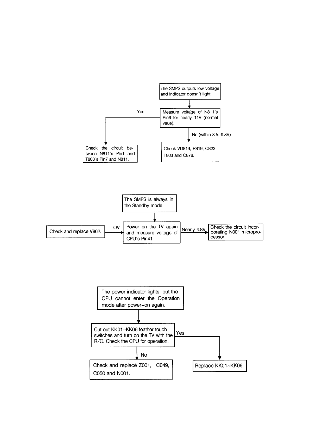
1.3 The SMPS outputs low voltage and indicator doesn’t light.
1.4 The power indicator lights but the SMPS is still in the Standby mode.
2. Control System
2.1 The power indicator lights, but the CPU cannot enter the Operation mode after power-on again.
40
Page 43

SERVICE MANUAL
TROUBLESHOOTING FLOW CHARTS (continued)
2.2 No character appears on the screen.
2.3 Channel number remains unchanged during auto program.
3. Video Signal Processor
3.1 No color
41
Page 44

SERVICE MANUAL
TROUBLESHOOTING FLOW CHARTS (continued)
3.2 The color is abnormal.
4. Horizontal/Vertical Scan Circuit
4.1 No raster
42
Page 45
SERVICE MANUAL
TROUBLESHOOTING FLOW CHARTS (continued)
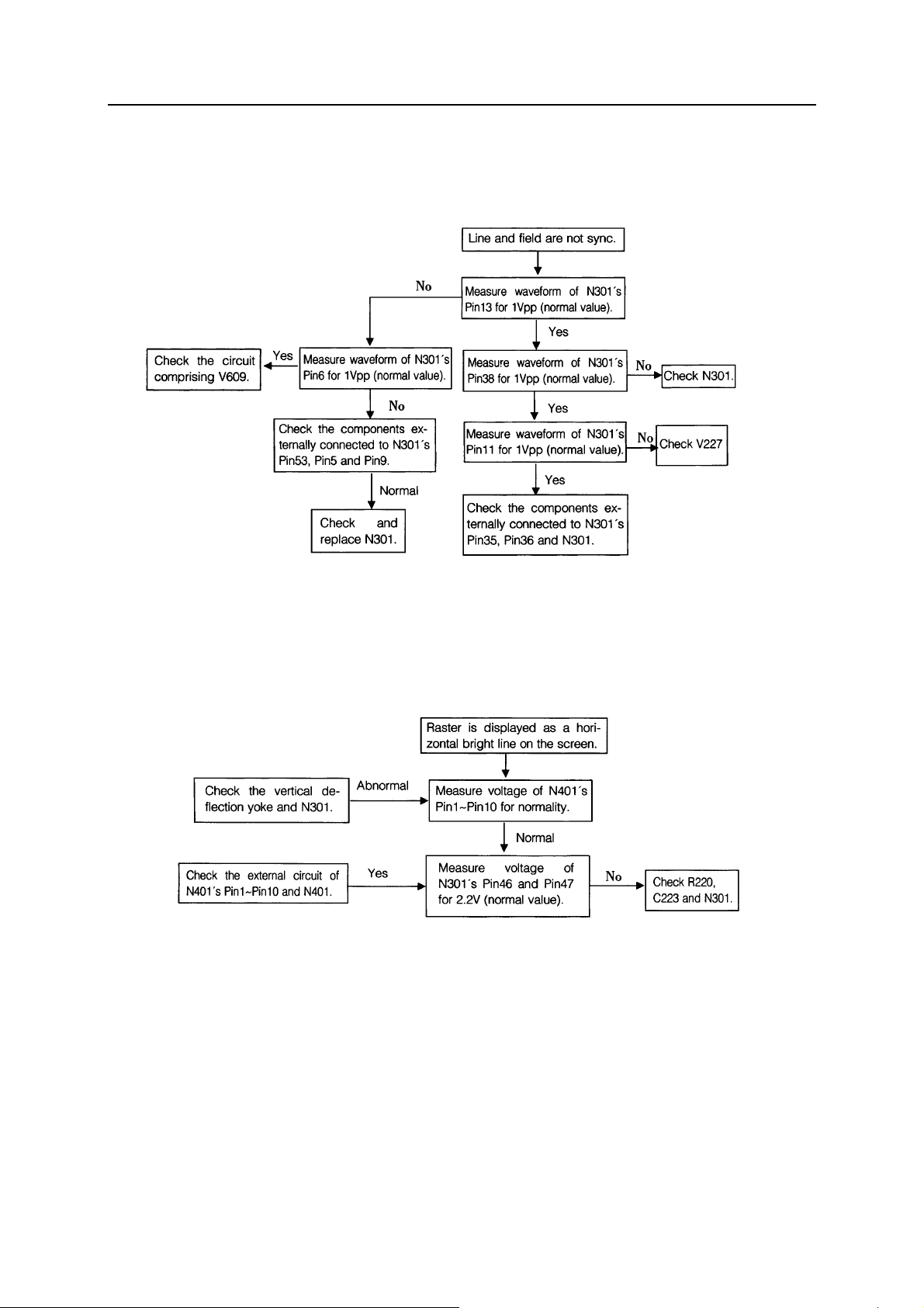
4.2 Line and field are not sync.
4.3 Raster is displayed as a horizontal bright line on the screen.
43
Page 46
SERVICE MANUAL
TROUBLESHOOTING FLOW CHARTS (continued)
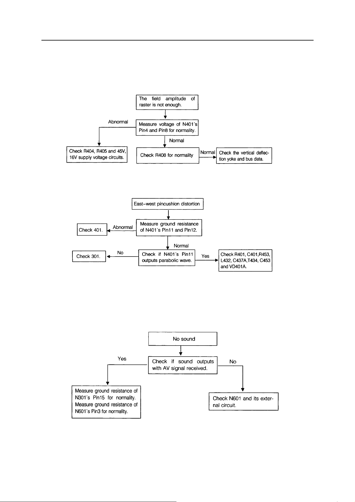
4.4 The field amplitude of raster is not enough.
4.5 East-west pincushion distortion
5. Audio System
5.1 No sound
44
Page 47

SERVICE MANUAL
SERVICE SPARE PARTS LIST
APPENDIX
1. CIRCUIT DIAGRAM
2. FINAL WIRING DIAGRAM
3. FINAL ASSEMBLY DIAGRAM
4. PRINTED CIRCUIT BOARD DIAGRAMS
45
Page 48

APPENDIX 1: CIRCUIT DIAGRAM OF AT2408 (1)
Page 49

APPENDIX 1: CIRCUIT DIAGRAM OF AT2408 (2)
Page 50

APPENDIX 1: CIRCUIT DIAGRAM OF AT2408S (1)
Page 51

APPENDIX 1: CIRCUIT DIAGRAM OF AT2408S (2)
Page 52

APPENDIX 2: MAIN PCB OF At2408
Page 53

APPENDIX 2: MAIN PCB OF AT2408S
Page 54

APPENDIX 2: PCB OF AT2408
CRT RGB PCB
AV P CB
POWER PCB
Page 55

APPENDIX 2: PCB OF AT2408S
CRT RGB PCB
AV P CB
POWER PCB
Page 56

APPENDIX 3: FINAL WIRING DIAGRAM OF AT2408
From Right Speak
Cord Plug
A
XP205
Cord Plug
Red
Black
To Degaussing Coil
DY PCB Assembly
XS802
XS804
XS805
XS804
Cord Plug
XS803
XP804
XS803
XSY03
XP804
Cord Plug
XP803
Cord Plug
XPK01
Cord Plug
XSK01XSK02
Main PCB Assembly
From Deflection Yoke
XS402
XPS06
XPK02
XPA04B
XSY01
XPA04A
From Left Speaker
B
Cord Plug
XP205
Cord Plug
Cord Plug
XPA04A
To CRT's Ground Wire
XPY01
CRT RGB PCB Assembly
GND2
GND1
XPY03
XPY03
Cord Plug
XPY01
Cord Plug
Page 57

APPENDIX 4: FINAL ASSEMBLY OF AT2408
Page 58

APPENDIX 4: FINAL ASSEMBLY OF AT2408S
Page 59

y
y
y
y
y
y
y
Group component lists of AT2408&AT2408S
Part name CRT Type
Remote control
Remote control
Remote control
Remote control
CRT assembly
CRT assembl
Front cover assembl
Back cover
Main PCB assembly
Main PCB assembly
Power PCB assembl
AV PCB assembl
AV PCB assembl
CRT RGB PCB assembl
Control PCB assembl
Old Part number
TYPE:K12C-C1; When using CH04T1002 CPU (for AT2408S only) K12C-C1
TYPE:K12K-C2; When using CH04T1009 CPU (for AT2408S only) K12K-C2
TYPE:K12B-C2; When using CH04T1002 CPU (for AT2408 only) K12B-C2
TYPE:K12L-C1; When using CH04T1009 CPU (for AT2408 only) K12L-C1
For IRICO or Shanghai Novel CRT 64SX505Y22-DC02
For LG CRT A59KYL220X08
For AT2408 only for AT2408 ONLY, JUC7.820.425-2,
JUC7.820.775
For AT2408S only for AT2408S ONLY, JUC7.820.425-2,
JUC7.820.775
For AT2408/2408S and KT2406 JUC7.820.427-1, JUC7.820.774
For AT2402S/AT2408S only JUC.820.426-3
For AT2408 only JUC.820.426-3
JUC7.820.428
JUC7.820.429
Page 60

New Part number List
8201800271L
8201801682L $15.00
8201800032L
8201800271L
8537000370C01
8537000370C02
8611604570C
8807400230C
8667206130C04
8667206130C05
8667206140C02
8667206160C01
8667206160C02
8667206150C01
8667206120C
$15.00
$15.00
$15.00
$98.00
$98.00
$43.26
$11.88
$102.00
$102.00
$23.82
$11.88
$11.88
$11.88
$28.80
Page 61
6/24/2003
APEX DIGITAL TELEVISION In-Warranty Schedule by Model
3
Carry-In
Service
In Home
LIMITED WARRANTY
1
Product Model No.
Remote
Control
2
13 inch
AT1302 90 90 90 90 N N N N/A N/A N/A N/A N/A
Labor
CRT
Stock
Repair
Yes/NoYes/No Yes/NoParts
REIMBURSEMENT RATES
Carry-In
Minor Major Minor Major Repair
Home Service
Stock
AT1308 90 90 90 90 N N N N/A N/A N/A N/A N/A
2
20 inch
AT2002 / AT2002S 365 90 90 365 N N N N/A N/A N/A N/A N/A
AT2008 / AT2008S 365 90 90 365 N N N N/A N/A N/A N/A N/A
GT2011J 365 90 90 N N N N/A N/A N/A N/A N/A
GT2011S 365 90 90 365 N N N N/A N/A N/A N/A N/A
GT2015 365 90 90 365 N N N N/A N/A N/A N/A N/A
GT2015DV 365 90 90 365 N N N N/A N/A N/A N/A N/A
KT2006
24 inch
2&3
1 YEAR STORE REPLACEMENT
AT2402 365 90 90 365 N N N N/A N/A N/A N/A N/A
AT2408 / AT2408S 365 90 90 365 N N N N/A N/A N/A N/A N/A
GT2411S 365 90 90 365
GT2415 365 90 90 365 N N N
PF2425 365 90 90 730 N N N N/A N/A N/A N/A N/A
KT2406 365 90 90 365 Y N N
2
25 inch
N/A N/A N/A N/A N/A
4444 4
AT2502 365 90 90 365 N N N N/A N/A N/A N/A N/A
AT2502S 365 90 90 365 N N N N/A N/A N/A N/A N/A
3
27 inch
AT2702 365 90 90 365 Y Y Y
AT2702S 365 90 90 365 Y Y Y
AT2708 / AT2708S 365 90 90 365 Y Y Y
GT2711S 365 90 90 365 Y Y Y
GT2715 365 90 90 365 Y Y Y
PF2725 365 90 90 730 Y Y Y
GT2715DV 365 90 90 365 Y Y Y
3
32 inch
AT3208S 365 90 90 365 Y Y Y
GT3215 365 90 90 365 Y Y Y
PF3225 365 90 90 730 Y Y Y
KT3226 365 90 90 730 Y Y Y
4444 4
4444 4
4444 4
4444 4
4444 4
4444 4
4444 4
4444 4
4444 4
4444 4
4444 4
PROJECTION
GB4308 365 90 365 730 Y Y Y
GB43HD09 365 90 365 365 Y Y Y
GB5108 365 90 365 730 Y Y Y
GB51HD09 365 90 365 365 Y Y Y
GB55HD09W
GB65HD09W 365 90 365 365 Y Y Y
1
Limited Warranty is printed on the last page of the owner's manual
365 90 365 365 Y Y Y
4444 4
4444 4
4444 4
4444 4
4444 4
4444 4
2 All defective units 13" - 25 "during the first 90 days of ownership will be exchanged at the original place of purchase. Dealer
may contact APEX to receive a Return Authorization from Apex for credit or exchange.
3 Should the picture tube fail during the In-Warranty period the product will be exchanged. The customer is responsible for the
Service Center diagnostic fee after the initial labor warranty period and for all packing, transportation and insurance charges.
4 See Master Dealer File for Rates for each Dealer
NOTE: All handling, packing, shipping or freight charges are the responsibility of the customer. 1
 Loading...