

Page 1
SERVICE MA NUAL
CM—313
COLOR VIDEO MON ITOR
■
M600
ADC
Page 2
O w e
QQQ
V ... Ρ 0 2ΠΓ
_______
ΓCRPC-14
715A299-
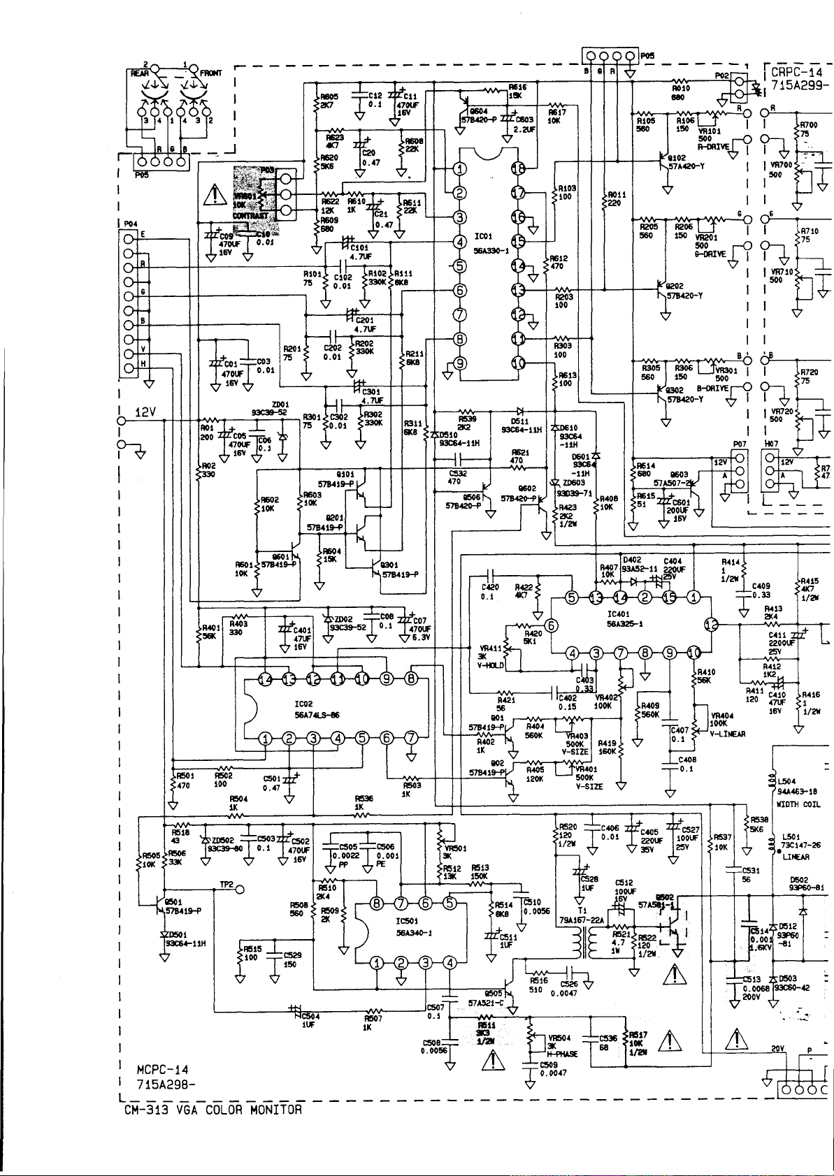
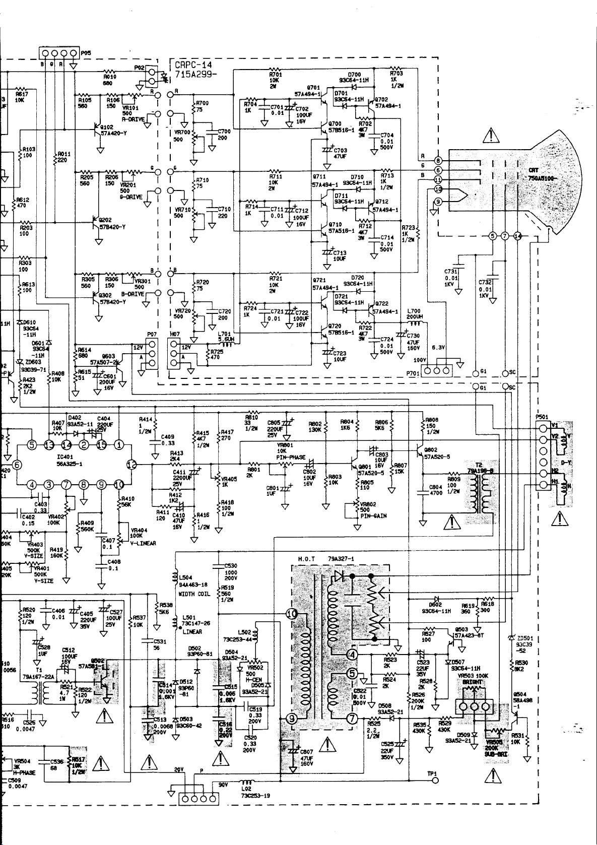
CM-313 VGA COLOR MONITOR
Page 3
ό ό ό ό 73C2S3 ·1 9 ____________________________________ 1
Page 4
4. ADJUSTMENT
4-1 ADJUSTMENT CONDITIONS AND PRECAUTIONS
1. Approximat ely 30 minu t e s sh ould be all o w e d f or warm up b efo re proceeding.
2. Adj u s t ments should be und e r ta k e n only on those necessary elements since mo st o f them have
been carefu l ly preset a t the f a ctory .
4-2 MAIN ADJUSTMENTS
NO.
1.
2.
3.
4.
5.
6.
7.
8.
9.
10.
11.
12.
13. HOR. CENTER
14.
15.
16.
17.
18.
FU N CTIO N LOCA TIO N DESIGNATION
B+ AD J PCB-POWER
R.G.B. D RIV E PCB - M A IN VR101, 201, 301
VERT . SI Z E FOR
ALL M O D E
VERT . SIZ E FOR
MODE 2
VERT . SIZ E FOR
MOD E 1
VERT . HO LD
VERT . LI NEAR PCB - M A I N
VERT. CEN TER
HOR. P INCUS HION GAI N
HOR. P I NCUS H I ON PHASE PCB - M A IN
HOR. H OLD
HOR. PHASE
HOR. WI DTH PCB - M A IN
SUB-BRI G HTNE S S
R.G.B. CUT - O FF CRT-B OARD VR700, 710, 720,
BRI GHTNESS
CONTRAS T
VR9 01
PCB - M A IN
PCB - M A IN
PCB-MAIN
PCB - M A IN VR4 1 1
PCB-MAIN
PCB-MAIN
PCB - M A IN
PCB -M A I N VR504
PCB - M A IN
PCB-MAIN
PCB - M A IN
PCB -M A I N
VR40 2
VR403
VR40 1
VR404
VR40 5
V R80 2
VR80 1
VR5 01
VR502
L501
VR50 5
VR508
VR6 0 1
4-3 ADJUSTMENT METHOD
1. Swit c hing regu la t o r un i t
(a) Conn e ct a DC v o ltag e mete r between TP1 and groun d , tha n adju s t VR90 1 to be 8 5Vdc.
Note : Do n ot opera te Switc hing re g u la t o r un it without a n y load.
2. Sub-Brightness: VR50 5
Measure CR T s o ck e t pin # 5 , adj us t VR505 t o be —3 2 V d c.
3. Hor. ho l d: VR-50 1
(a) Con n e ct TP2 t o gro und .
(b) Adj ust VR5 0 1 until th e bars (moving bars) are v ertica l and no t s la n tin g to l eft or right.
(c) D is co n n ec t TP 2 from groun d , th e n VR501 is a djusted p r o p erly.
-7 -
Page 5
4. Hor. ce nt e r: VR502
Adjust VR502 until the raster is ju st located at ce n t e r of the panel.
(If raster is t oo dim, Adjust the screen VR of F LY-b ack transformer u ntil raster can be seen)
5. Hor. phase: V R504
Adjust VR 504 until the disp la y p i c t ure is located at t h e center of raster.
6. Hor. width: L501
Adjust h orizo ntal w idt h c oil L501 so that th e size of p i cture is 240m m
7. Vert ic a l linear : VR4 04
(a) Select a cross-hatch pattern .
(b) Adjust VR404 so that ve rt ic a l l inea r i t y is optim um.
8. Ver t ic a l size: VR401, 402, 40 3
Ver t i cal has thr ee modes, (m od e 1, 2, 3,)
(a) At F ir s t, use mode 3, signal that has vertic a l freq u e ncy 6 0 Hz a dj u s t VR402 so that v ert ica l
vertical size is 1 80 m m .
(b) Change t o mo d e 2, ad ju s t VR403 so that v e r t ic a l size is 180 mm
(c) Change to m o de 1, a d j u st VR 4 0 1 so that ver t ic al size is 1 80 m m .
9. Pincush ion adju s t m ent:
(a) Using crosshatch pa tt e r n , adju s t VR8 0 1 fo r symmetry between up-do w n side.
(b) A djus t VR802 for straight v e r tical lines on b o t h sides.
10. V e r t ical Center: V R40 5
Adjust VR 405 to c e n te r th e p icture verti c ally.
11. V e r t ic al Ho l d : VR 4 0 1
Using any p a t te r n gen era to r that has ve rt ic a l fre quen c y 50 H z and a p p l y to this monit o r. I f a
displa y quivers u p w a r d or downw a r d, t urn VR40 1 on the main PCB t o st ab iliz e it.
12. White balance:
A. In i t ial set up.
(a) Disable th e v id e o i nput signal.
(b) V R10 1, 201, 301, 700 , 71 0, 720 , set to mid dle p ositio n .
(c) Warm up more than 15 m in ut es .
- 8 -
Page 6
B. Bias adjustment.
(a) Adj ust G2 potentiome ter, check which color is first to appear, then turn c ut- off VR of that color
(VR700, 710, 720,) to min imu m, Again, turn G2 to more light An ot he r color appears, use this
cu t:o ff VR tor base.
(b) Using a Oscilloscope, adjust the base cu t- of f VR, so that the black level is 85Vdc.
(c) Ad just another tw o c u t-o ff VR until a faint neutral w hi te raster is produced.
C. Gain adjustment
(a) Enable all three channels (R. G. B.) to give a cross-hatch pattern on the screen.
(b) Using a oscilloscope, adjust the base drive VR (the same channel as B-(a) ), so that the
amplitude is 50Vp-p.
(c) Change the pattern to paper w hite video, turn contrast control to minim um, adjust the
luminance is 4 f t / l (fostlambert).
(d) Using a T V colo r analyzer, adjust the othe r tw o c u t-o f f VR (except the base c ut- of f V R) fo r a
white video corresponding t o a colo r temperature o f 930 0° K
(e) Tu rn contrast cont rol so that the luminance is 20 f t/ l , adjust the other two drive VR fo r the
same c olo r temperature.
(f) A few reiterations may be required to set the c olo r temperature the same at 4 f t /L and 20 f t / L
luminance level.
(g) Tu rn G2 contro l fo r raster to just appear (1 ft/l ).
13. Focus adjustment
Turn the contrast co ntro l to maximu m and set the brightness contro l to a suitable position, adjust
the focus control to the op tim um position.
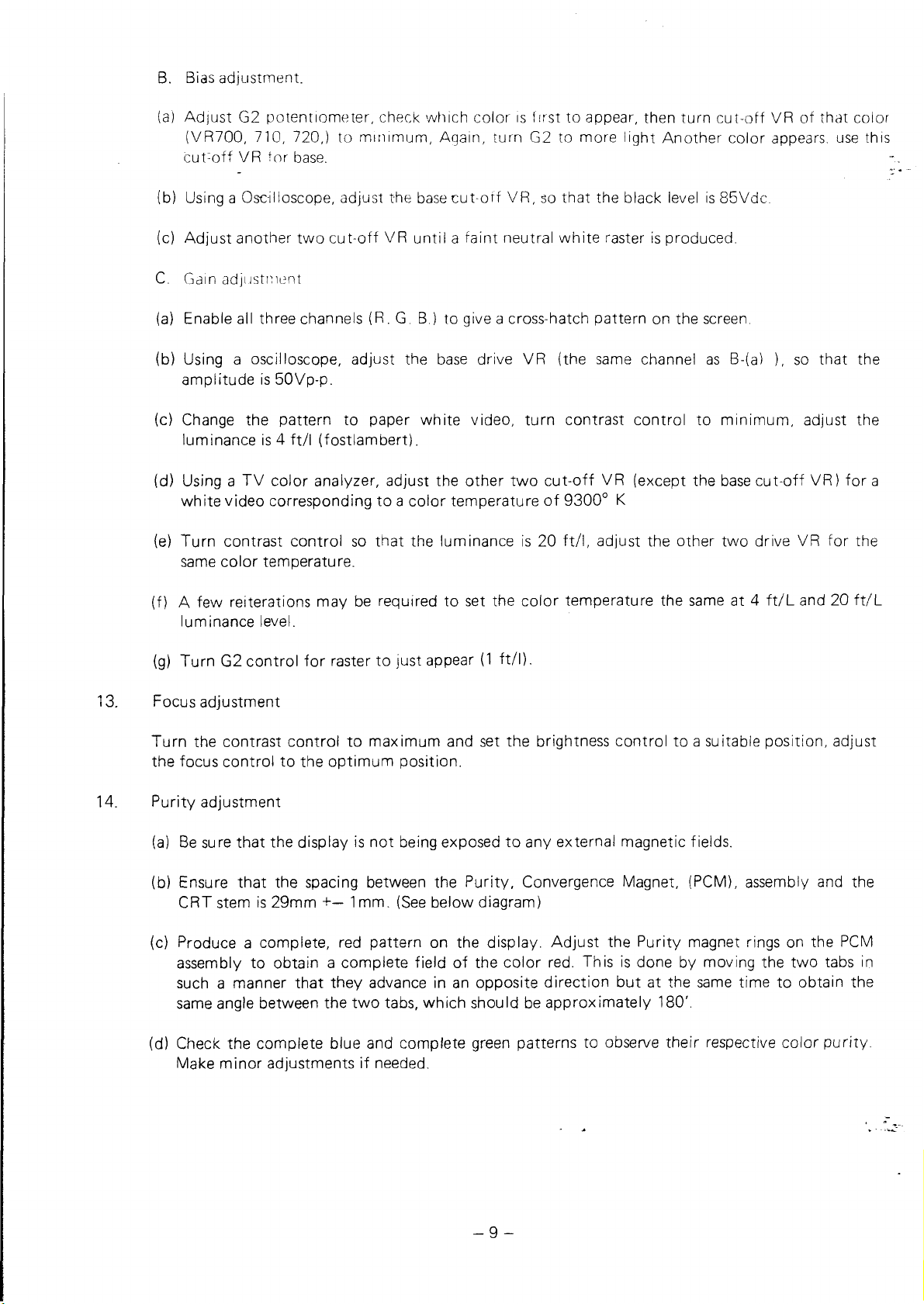
14. Purity adjustment
(a) Be sure th at the display is no t being exposed to any external magnetic fields.
(b) Ensure tha t the spacing between the Purity, Convergence Magnet, (PCM), assembly and the
CRT stem is 29mm +— 1 mm. (See below diagram)
(c) Produce a complete, red pattern on the display. A dju st the Purity magnet rings on the PCM
assembly to obtain a complete field of the colo r red. This is done by moving the two tabs in
such a manner t hat they advance in an opposite d irect ion but at the same time to obtain the
same angle between the tw o tabs, which should be approx ima tely 180'.
(d) Check the complete blue and complete green patterns to observe their respective colo r pur ity.
Make min or adjustments if needed.
- 9 -
Page 7
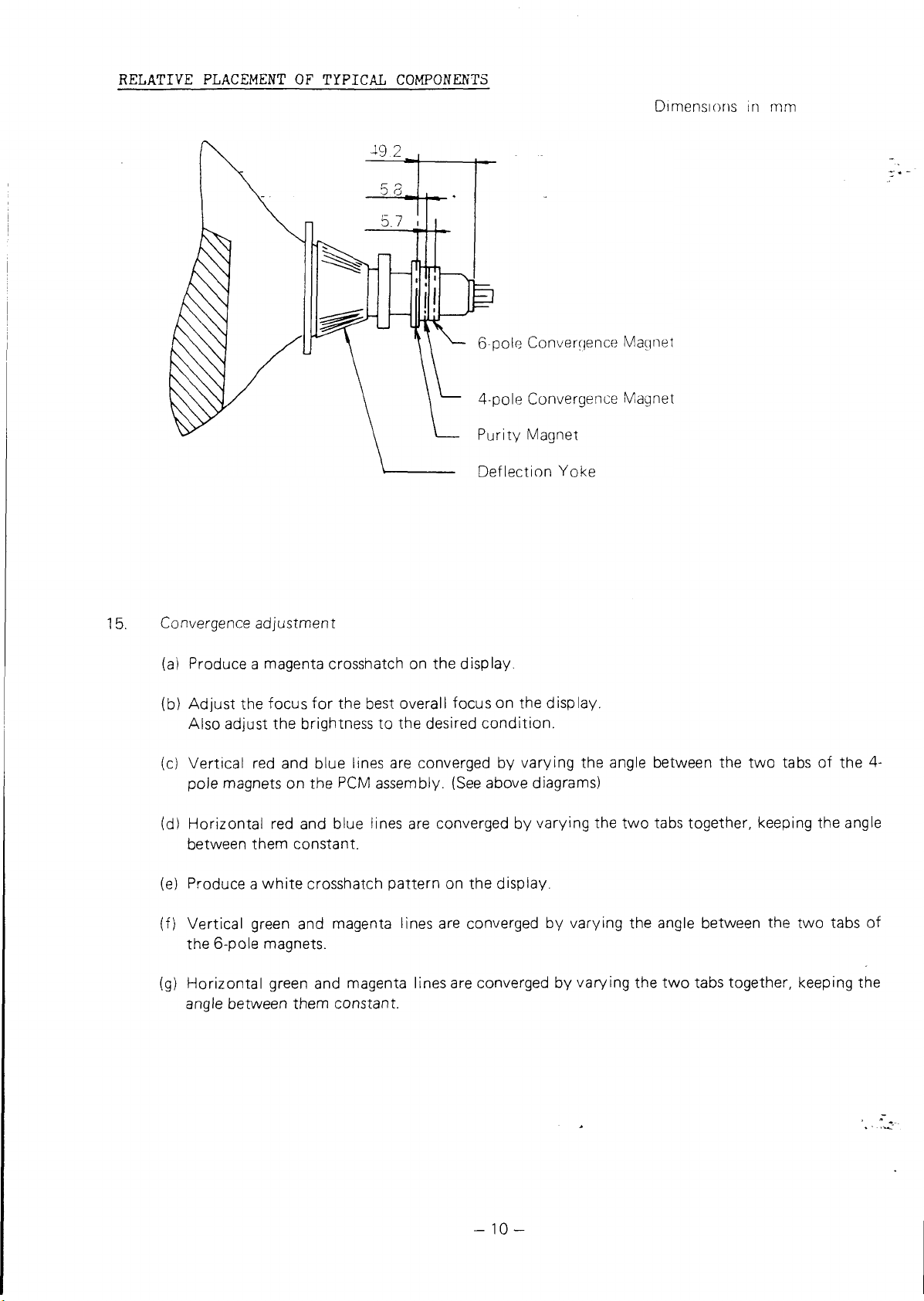
RELATIVE PLAC EMENT OF T YP ICAL COMPO N ENTS
Dimensions in mm
15. Convergence adjustment
(a) Produce a magenta crosshatch on the display.
(b) Adjust the focus for the best overall focus on the display.
Also adjust the brightness to the desired c ondit ion .
(c) Vertical red and blue lines are converged by varying the angle between the tw o tabs of the 4-
pole magnets on the PCM assembly. (See above diagrams)
(d) Horizontal red and blue lines are converged by varying the two tabs together, keeping the angle
between them constant.
(e) Produce a w hi te crosshatch pattern on the display.
(f) Vertical green and magenta lines are converged by varying the angle between the two tabs of
the 6-pole magnets.
(g) Horizontal green and magenta lines are converged by varying the t wo tabs together, keeping the
angle between them constant.
- 10 -
Page 8
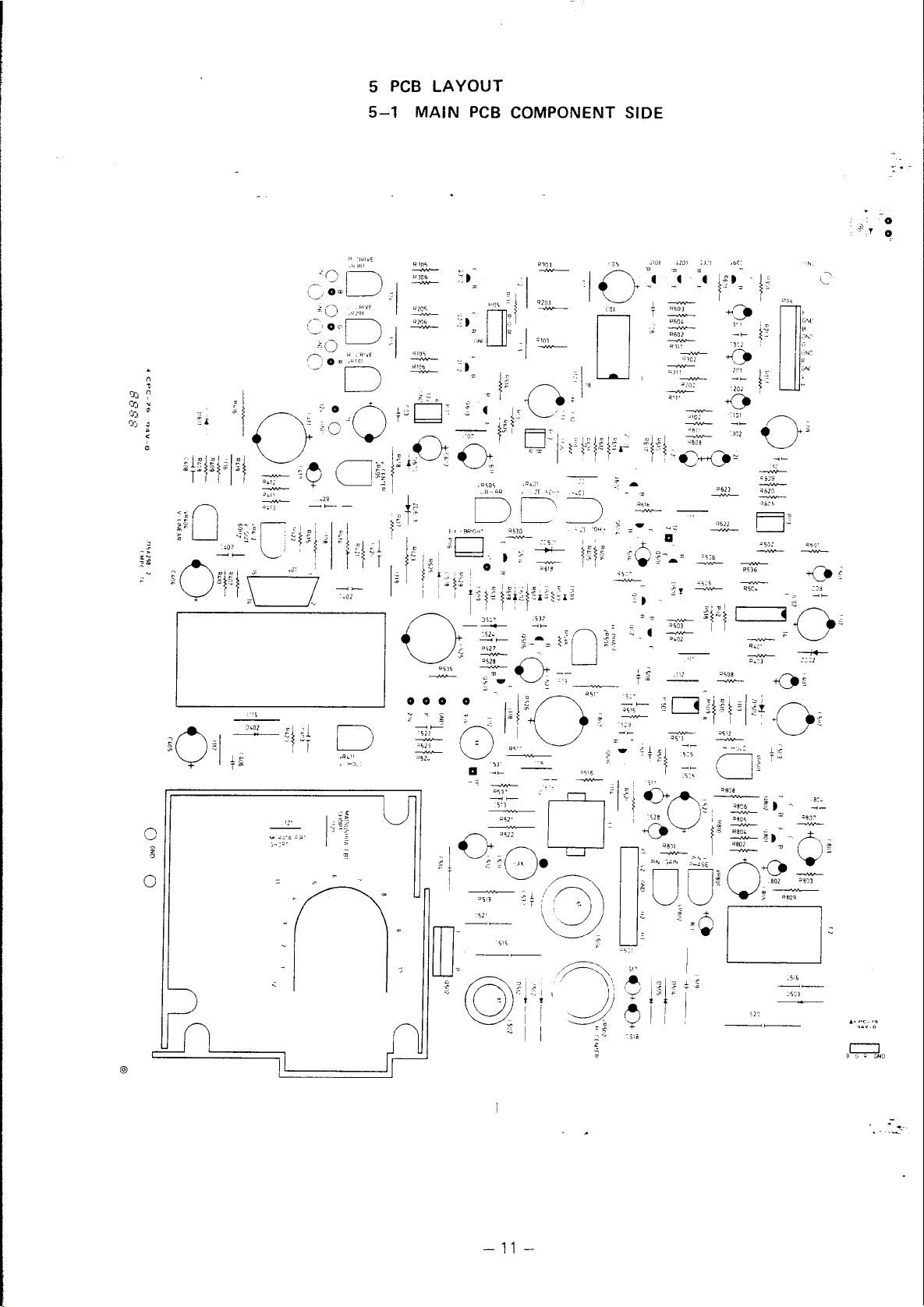
5 PCB LAYO U T
5-1 MA I N PCB COMPO NENT SIDE
ί'ΟΙ
»e>a l |
R 6 0 2 —I - ^2
" l'"2 :
-7ο Γ I ' -
- 11 -
Page 9
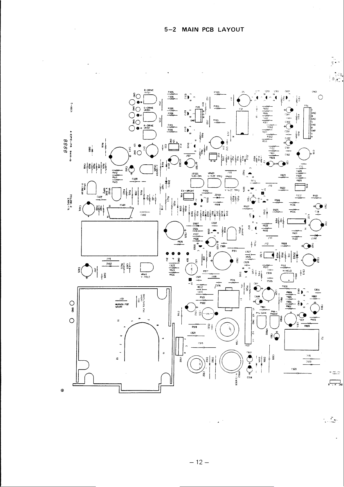
5- 2 MAIN PCB
LA Y O U T
35 V " ·:?ηι 'n ot op(v
'
20
:
9205
P206
310S
R106
• j Q . · μ> :
rot
.. A „
ϊ o
? --DO 2 - th - £2
"3^ C3°2 ]
"‘Of)?*
i?2t i C?0> I u
- v H T ~ « Γ r
c i r I „
3S88
O
GNO
Θ
GNO
GNO
R
GNO
- 12 -
Page 10

5- 3 SMPS CO M PO NE NT SIDE
- 13 -
Page 11

5- 4 SMPS LAY O U T
Page 12

S
o
—v o £
-*
C904 f
C903 t
' .*— 11— -
, · a s , -
• ί I s .
-m -
αίοί
B
—
-------------
'■” c 'l" Q 90t '
. . . . J .· ··-■>.. ,8 « ^ ε · ; v . 1 · . .
Si r e' s Γ Τ ‘i — · ' fe *mi't ‘ is
w- " X - Λ25 \ ..-> K > . m.§mgU)' „’ t „ " r | S
-if , \ ' Jttt*. £* v,· si a - '.a Ms, . ^ιλ l
* ■ \ f—^ —c if- S? 3 | ^ k g j ϊέ ' *
----------------------
c_«
' ' ’ ’ 8 Λ * '■: g l i VR901 I
i W i ; .
n u n m ' : n .« * \
Q ,
■'
o ,
η
C901
f
[ > % || I
in
I
Page 13

5- 5 C RT BOAR D PCB L A Y O U T & COMPONENT SIDE
- 16 -
Page 14

6. BLACK D IAGRAM
Page 15

CM-313
BLOCK DIAG RAM
Page 16

1 NO RASTER
CHECK 8 5 V LINE
ON M A IN PCB
7. T R OUB L E-SH OO TING
NG
------------>
OK
V
CHECK 100V LINE
ON M A IN PCB
NG
-----------------^
OK
V
CHECK 24 V LINE
ON M A IN PCB
NG
OK
LOA D SHORT
CIR C U IT
_____\k_
REPLACE SW.
REG. UN I T
LOA D S HORT
CIR C U IT
_____ψ____
REPLACE SW.
REG. UN IT
->
LOA D SHO RT
CIR C U IT
NO
____
NO
YES ^
-----------^
YES CHECK Q702, Q712
T CO
----------
CHECK Q502, D512
D502, C521, C515
Q722, Q701, Q7 1 1
721, Q700, 07 1 0
Q720,
- >
CHECK 05 05 , Q802
IC401
--
CHECK 12V LINE
ON M A I N PCB
OK
V
CHECK 6.3 V LINE
ON CRT PCB
OK
_______
CRT OR FBT
FA I LU RE
y/_ ___
NG
NG
_ _ _ _ _ _ V -
REPLACE SW.
REG. UN IT
LOA D SHORT
CIR C U IT
_____±____
REPLACE SW.
REG. UN IT
LOA D SHO RT
— >
CIR C U IT
. . J l .
REPLACE SW.
REG. UN I T
NO
____ _
NO
YES CHECK IC501, IC01
Q101, 0 2 0 1 , 0 3 01
YES
CRT H EATER
>
FA IL U R E
Page 17

7 -2 PICTURE OR SOME COLOR MISSING
CHECK SIG N AL CABLE
-CONNECTOR
OK
CHECK Q602 NG
OK
V
CHECK IC02,
PIN ip 3
OK
CHECK IC01
NG
-------------------->
NG
----------
NG
REPLACE S IG N A L
CABLE
REPLACE Q602
REPLACE IC02
»
REPLACE IC01
OK
CHECK Q102, Q202, Q302, 06 03 , Q7 01 , 071 1 , 0 721 ,
R700, R710, R720, R702, R712, R722,
- 19 -
Page 18

7-3 NO V E R T . SCAN (ONE HOR. L IN E RAST ER)
CHECK IC401
OK
t
\
CHECK IC02
OK
\
/
CHECK
Q01 , Q02
- 20 -
Page 19
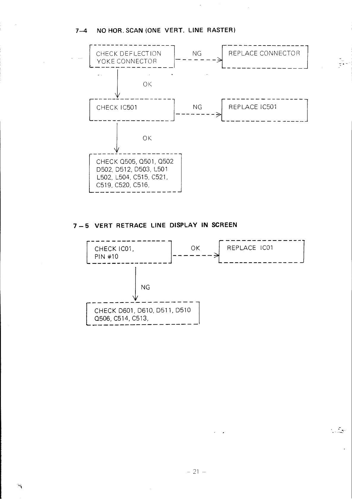
7-4 NO HOR. SCAN (ONE V E RT. LINE RASTE R)
CHECK
YOKE
CHECK IC501
DEFLEC TION
CONNECTOR
OK
\
/
OK
NG
V
CHECK 0 5 05 , Q501, Q502
D502, D512, D503, L501
L502, L504, C515, C521,
C519, C520, C516,
7 - 5 VERT RETRACE LINE DISPLAY IN SCREEN
CHECK IC01,
PIN #10
--- - --- - --
NG
____________
y_____________________
CHECK D6 01 , D610, D511, D510
Q506, C514, C513,
OK
REPLACE IC01
>
- 21 -
Page 20
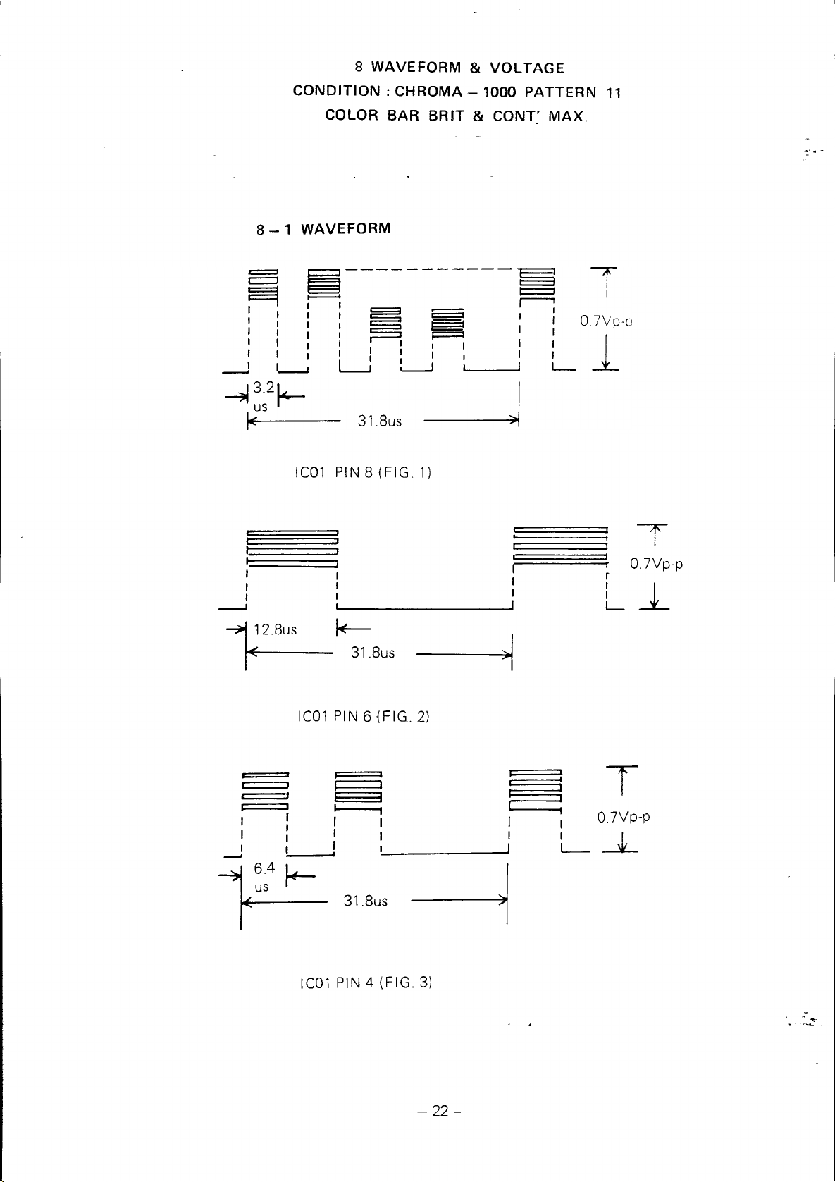
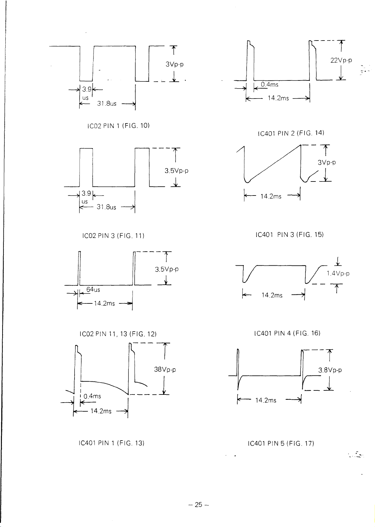
8 WA VE FO RM & V O LT AG E
CO N DIT IO N : C HR OM A - 1000 PAT TER N 11
COLOR BAR BRIT & C ON T' MAX .
8 - 1 WAVEF OR M
IC01 PIN 8 (FI G.1)
12.8us k
<
--------------- 31.8us
IC01 PIN 6 (F IG. 2)
6.4
k -
us
<
----------------
-----
I
31.8us
T
0.7Vp-p
J L
IC01 PIN 4 (FIG. 3)
- 22 -
Page 21
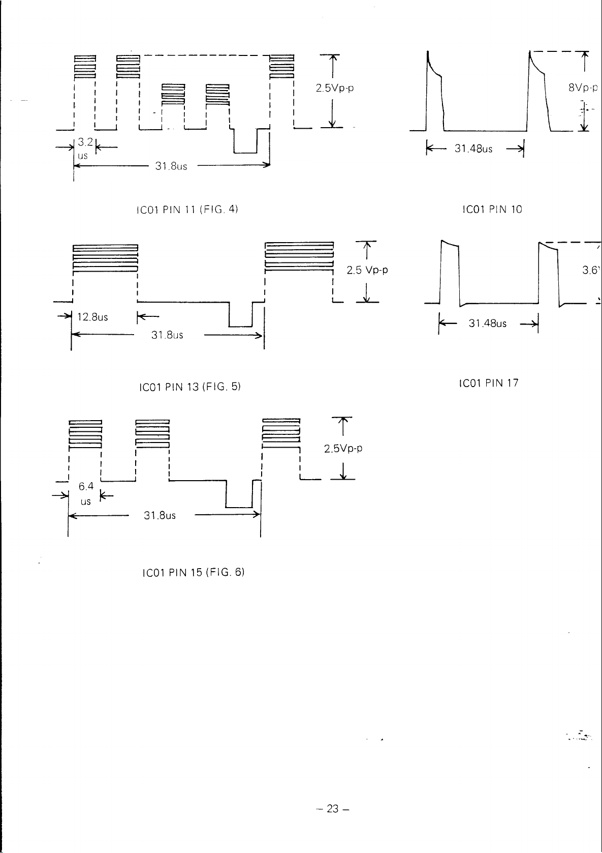
2.5Vp-p
I * - 31.48us Η
12.8us
"£
---------
6.4
us
I*-
IC01 PIN 11 (FIG. 4)
h —
31.8us
IC01 PIN 13 (FIG. 5)
31.8us
T
1 2.5 Vp-p
L
JL J
T
2.5Vp-p
A .
IC01 PIN 10
3.6'·
✓
j*— 31.48us — >|
IC01 PIN 17
IC01 PIN 15 (FIG. 6)
- 23 -
Page 22
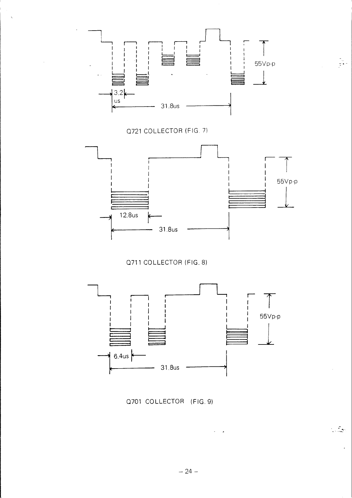
Q721 CO LLE CT OR (FIG. 7)
1
12.8us
t
----------------
0711 COLLEC TOR (FIG. 8)
— 31.8us
/ \
55Vp-p
/
~ P T
55Vp-p
6.4us [*
it-
---------------------
------
31.8us
Q701 COLLE CTOR (FIG. 9)
- 24 -
Page 23
' T
3Vp-p
Ps
I V " " “ T
22Vp-p
3.9
us
IC02 PIN 1 ( FIG. 10)
3.9 L _
US
IC02 PIN 3 (FIG. 11)
64us
. 1 .
3.5Vp-p
. A .
'"T
3.5Vp-p
j .
0.4ms
IC401 PIN 2 (FIG. 14)
IC401 PIN 3 (FIG. 15)
μ
1
1,4Vp-p
T
IC02 PIN 11, 1 3( FI G . 12)
IC401 PIN 1 (FIG. 13)
IC401 PIN 4 ( FI G . 16)
“T
3.8Vp-p
C Il
\f— 14.2ms ------
IC401 PIN 5 (FIG. 17)
- 2 5 -
Page 24
h - 14,2ms -A
“ T
3.2Vp-p
_ 1
23Vp-p
IC401 PIN 6 (FIG. 18)
|*— 14.2ms - ^ |
IC401 PIN 9, 10 (FIG. 19)
Ji:— 14.2ms —
IC401 PIN 15( FI G. 22)
0.8Vp-p
______
31.8us -*|
IC501 PIN 1 (FIG. 23)
4.1 Vp-p
6u s h~
IC401 PIN 12 (FIG. 20)
" T
13 Vp-p
. 1
IC 401 PIN 13 (FIG. 21)
IC501 PIN 3 (FIG. 24)
IC501 PIN 4 (FIG. 25)
- 26 -
Page 25
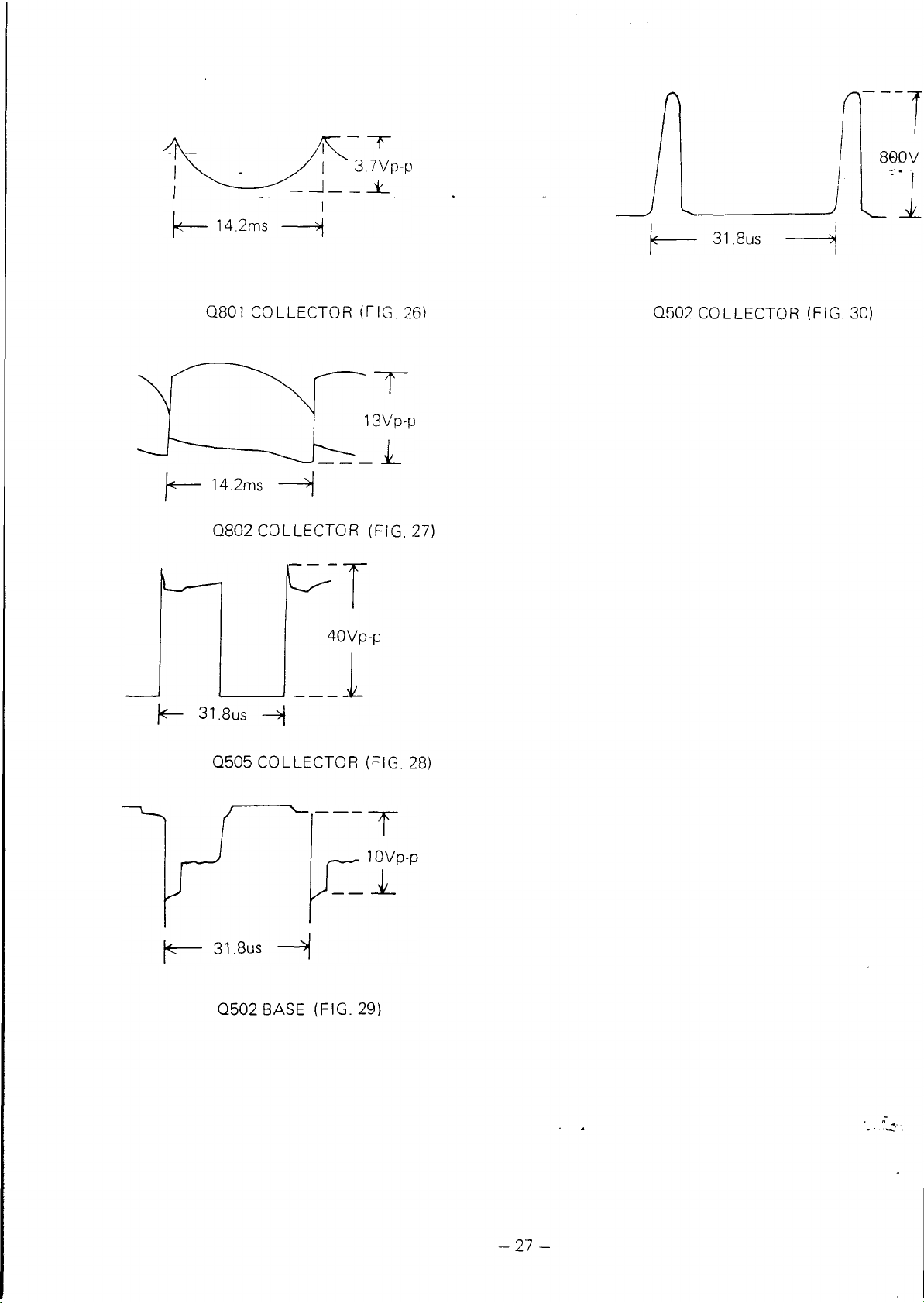
Q801 CO LL ECT OR (FIG. 26) 05 0 2 C OL LEC TO R (FIG. 30)
j*
-----
14.2ms
08 0 2 C OL LE CTO R (FIG. 27)
-----
05 0 5 COL LEC TO R (FIG. 28)
05 0 2 BASE (FIG. 29)
- 27 -
Page 26

8 - 2 DC VO LT AG E
1. IC01 2. IC02
#
1
: 12V
PIN #
1
: 3.6V
#
2
: 4.3 V
#
3
: 6V
4
#
: 2 .3V
#
: 0V #
5
#
: 2.3V
6
# 7 : OV
# 8 : 2.3V
#
#
# 11 :
# 12 :
# 13 :
OV
9 :
10 : 1.96V
1.4V
OV
1.5V
+ r
2 : 3.6V
■U·
ΤΓ
3
: 0.6V
# 4
: 5.1 V
: 3.67V
5
• u.
Tt
: 0.2V
6
£
7 : OV
8 :; 3.6V
#
# 9 : 5.1V
10 :
#
0.28V
# 11 : 0.15V
# 12 : 0.2 8V
13 : OV
#
14 :
#
#
15 :
# 16 :
17 : 1.25V
#
18 :
#
OV
1.5V
OV
12V
14 :
#
5.1V
- 2 8 -
Page 27

IC501
4. IC401
PIN # 1
# 2
# 3
# 4 : 2.3V
# 5
# 6 : 9.4V
# 7 : 4.2V
# 8 : 3.8V
: 0.5V
: OV
: 2.7V
: 5.4V
PIN # 1
# 2
# 3
# 4: : 0.4V
# 5
# 6
# 7
# 8 :
# 9 :: 5.5V
# 10
# 11 :
# 12 :
: 11.5V
: 20 V
: 2.6 V
: OV
: OV
: 6 .6V
: OV
: 6.0 V
4.3V
4.0V
# 13 :
# 14 :
# 15 :
0.3V
20V
0.8V
- 29 -
Page 28

TRANSISTOR
Q601 B : OV
- C
Q506 :
E
E
B
C
: OV
: OV
: 1.1V
: 1.3 V
: OV
Q602
Q603
: B
C
E
: 1.28 V
: 0 .6V
C : OV
E
: 1.5V
B
: 0.8 8V
: OV
E : 0.7V
Q801 : B : 1.3V
C : 16V
E
: 18.4V
Q505 :
B
: 0.46 V
C : OV
E
: 2.7V
Q504 :
Q701 :
B : 2.1V
: 2.7V
C
E
11.5V
12V
B
C 70V
E
11.5V
Q711 :
12V
B
70V
C
E 11.5V
Q721 :
12V
B
70V
C
Q802
Q503
Q501 :
Q702 :
Q712 :
Q722 :
E
: 15.1V
B
: 14.5V
C : 4 .5V
E
: OV
B : OV
C
: 7.0V
E
: 0.3 V
B
: 0 .4V
C : 4 .8V
E
69.3V
B
70V
C 9 7V
E
69.3V
B
70V
C 97V
E 6 9.3 V
B
70V
C
97V
E : 2.1V
C :
1.4V
OV
Q102 : B :
E : 2.1V
Q202 :
B :
C :
1.4 V
OV
E : 2.1V
C :
E :
B :
C :
E :
B :
C :
1.4V
OV
2.3V
OV
5.1V
2.3V
OV
5.1V
Q302 : B :
Q1Q1 :
Q301 :
D 5 08anod e : - 230V
ZD01 cathode : 5.1 V
ZD502 cathode : 9.4V
- 3 0 -
E :
1.5V
Q700 :
B :
C :
2.2V
11.5V
E : 1.5V
Q710 : B : 2.2V
C :
11.5V
E : 1.5V
Q720 : B : 2.2 V
C :
11.5V
E : 2.3V
Q201 :
B :
OV
C : 5.1 V
E : 2 .3V
Q201 :
B : OV
5.1V
C :
Page 29

1 1 -1 SW ITCHING POWER D IA GR AM
Page 30

NOTE:
C901
L901
C902
C903
C904
CSSO
CS32
J902
TUV/Z2F
1UF
73C150-5A
4700
4700
4700
4700
CONNECTED
UL/FCC
0.1UF
73C150-5A
O.lUF
4700
4700
4700
CONNECTED
SWITCHING POWER D IAG R AM
 Loading...