

Page 1
LM-729 Service Manual Rev: A
SERVICE MANUAL
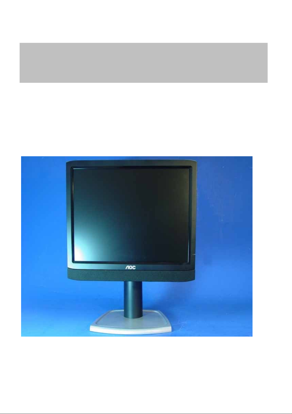
17” LCD Monitor
LM-729
THESE DOCUMENTS ARE FOR REPAIR SERVICE INFORMATION ONLY. EVERY REASONABLE
EFFORT HAS BEEN MADE TO ENSURE THE ACCURACY OF THIS MANUAL; WE CANNOT
GUARANTEE THE ACCURACY OF THIS INFORMATION AFTER THE DATE OF PUBLICATION
AND DISCLAIMS RE LIABILITY FOR CHANGES, ERRORS OR OMISSIONS.
Page 1 of 61
Page 2

LM-729 Service Manual Rev: A
Prepared: Shiwei
Date: Jul-30-03
Page 2 of 61
Page 3
LM-729 Service Manual Rev: A
Revision History
Revision Date Page Items Modification
A Date:Jul-30-03 All First version release;
Page 3 of 61
Page 4

LM-729 Service Manual Rev: A
Table of Contents
Table of Contents ---------------------------------------------------------------------------------------------------3
1. MONITOR SPECIFICATIONS ---------------------------------------------------------------------------5
2. LCD MONITOR DESCRIPTION ---------------------------------------------------------------------------6
3. OPERATING INSTRUCTIONS ---------------------------------------------------------------------------7
3.1 GENERAL INSTRUCTIONS -------------------------------------------------------------------------7
3.2 CONTROL BUTTONS ------------------------------------------------------------------------------------7
3.3 ADJUSTING THE PICTURE--------------------------------------------------------------------------------7
4. Input/Output Specification - -------------------------------------------------------------------------------10
4.1 Input Signal Connector --------------------------------------------------------------------------------10
4.2 Factory Preset Display Modes -------------------------------------------------------------------------- 11
4.3 Power Supply Requirements ------------------------------------------------------------------------ 12
4.3.1 Input Requirements -------------------------------------------------------------------------------------12
4.3.2 Output Requirements ------------------------------ ------------------------------------------------12
4.4 PANEL SPECIFICATION -------------------------------------------------------------------------------14
4.4.1 Panel Feature ------------------------------------------------------------------------------------------14
4.4.2 Display Characteristics --------------------------------------------------------------------------------14
4.4.3 Optical Characteristics -------------------------------------------------------------------------------14
4.4.4 Parameter guide line for CCFL Inverter ------------------------------------------------------14
5. Block Diagram ------------------------------------------------------------- -----------------------------15
5.1 Monitor Exploded View ------------------------------------------------------------------------------------15
5.2 Software Flow Chart -------------------------------------------------------------------------------------16
5.3 Electrical Block Diagram ------------------------------------------------------------------------------18
5.3.1 Main Board -------------------------------------------------------------------------------------------------18
Page 4 of 61
Page 5

LM-729 Service Manual Rev: A
5.3.2 Inverter/Power Board -------------------------------------------------------------------------------------19
6. Schematic -------------------------------------------------------------------------------------------------------21
6.1 Main Board -----------------------------------------------------------------------------------------------21
6.2 AUDIO Board -----------------------------------------------------------------------------------------25
6.3 Key Board ------------------------------------------------------- ---------------------------------------26
6.4 Inverter/Power Board -----------------------------------------------------------------------------------27
7. PCB Layout -------------------------------------------------------------------------------------------------29
7.1 Main Board -----------------------------------------------------------------------------------------------29
7.2 Inverter/Power Board -----------------------------------------------------------------------------------31
7.3 Keypad Board And Audio board-------------------------------------------------------------------------34
8. Maintainability --------------------------------------------------------------------------------------------------34
8.1 Equipments and Tools Requirements ----------------------------------------------------------------35
8.2 Trouble Shooting ---------------------------------------------------------------------------------------------33
8.2.1 Main Board --------------------------------------------------------------------------------------------------35
8.2.2 Power/Inverter Board -------------------------------------------------------------------------- ----------38
8.2.3 Key Pad Board ---------------------------------------------------------------------------------------------40
9. White-Balance, Luminance adjustment ----------------------------------------------------------------41
10. EDIT Content -------------------------------------------------------------------------------------------42
11. BOM List -------------------------------------- -----------------------------------------------------------------43
Page 5 of 61
Page 6
LM-729 Service Manual Rev: A
1.MONITOR SPECIFICATIONS
Driving system TFT Color LCD
LCD Panel Size 43.2cm(17.0")
Pixel pitch 0.264mm( H )x 0.264mm( V )
Viewable angle 90˚ (H) 90˚ (V)
Response time (typ.) 25 ms
Video Analog /Digital
Input Sync. Type H/V TTL
H-Frequency 30kHz – 80kHz
V-Frequency 55-75Hz
Display Colors Over 16 million Colors
Dot Clock 135MHz
Max. Resolution 1280 x 1024
Plug & Play VESA DDC2BTM
Power Consumption ON Mode
OFF Mode
Maximum Screen Size
Power Source
Environmental
Considerations
Weight (N. W.) Packaged 7.0Kg Unit
Unpackaged 6.0Kg Unit
Operating Temp: 0°C to 40°C
<45W
<2W
Horizontal : 13.3”(337.92mm)
Vertical : 10.6”(270.336mm)
100~240VAC,47~63Hz
Storage Temp.: -20°C to 60°C
Operating Humidity : 15% to 90%
Page 6 of 61
Page 7
LM-729 Service Manual Rev: A
(
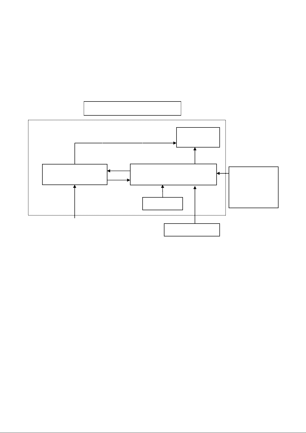
2. LCD MONITOR DESCRIPTION
The LCD MONITOR will contain a main board, an inverter/power board, keypad board , Audio board and
external power adapter which house the flat panel control logic, brightness control logic and DDC.
The Inverter board will drive the backlight of panel and the DC-DC conversion.
The Adapter will provide the 12V DC-power to inverter/power board.
Monitor Block Diagram
CCFT Drive.
Flat Panel and
CCFL backlight
Power board
include:adapter,inverter)
Keyboard
Main Board
RS232 Connector
For white balance
adjustment in
factory mode
AC-IN
100V-240V
HOST Computer
Video signal, DDC
Page 7 of 61
Page 8
LM-729 Service Manual Rev: A
3. OPERATING INSTRUCTIONS
3.1 GENERAL INSTRUCTIONS
Press the power button to turn the monitor on or off. The other control buttons are located at front panel of the monitor. By
changing these settings, the picture can be adjusted to your personal preferences.
The power cord should be connected.
-
Connect the video cable from the monitor to the video card.
-
Press the power button to turn on the monitor, the power indicator will light up.
-
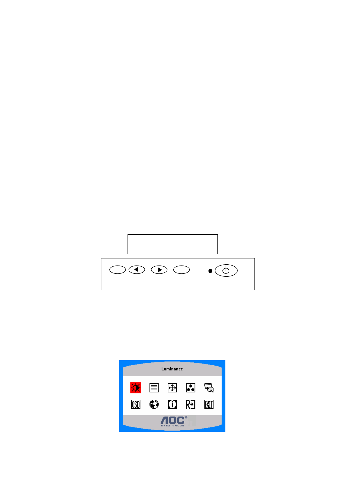
3.2 CONTROL BUTTONS
Power Button:
-
When pressed, the monitor enters the off mode, and the LED turns blank. Press again to restore normal status.
- Left / Right Button:
When the OSD show on screen, Left/Right Button are used to control the monitor functions. Press to switch functions or adjust
settings. And if the OSD off, Left/Right buttons are used to control the audio volume;
- Auto Adjust Key:
The Auto Adjust Key is used to automatically set the H Position, V Position, Clock and Phase.
- Power Indicator:
Green — Power On mode.
Orange — Power Saving mode.
Blank —Power Off Mode.
CONTROL Buttons
A B C D E F
Auto Volume Menu LED Power
A. Menu button
B. Left button/Volume down
C. Right button/Volume up
D. Auto button/Exit
E. Indicator light
F. Power button
3.3 ADJUSTING THE PICTURE
Page 8 of 61
Page 9
LM-729 Service Manual Rev: A
OSD Table:
Main
Menu Item
Luminance
Setup
Position
Color
Main
Menu Icon
Sub Menu
Item
Contrast
Brightness
Focus
Clock
H. Position
V. Position
Warm N/A Recall Warm Color
Sub
Menu
Icon
Description
Contrast from Digital-register. 0-100 Recall Cool
Backlight Adjustment 0-100 Recall Cool
Adjust Picture Phase to reduce
Horizontal-Line noise
Adjust picture Clock to reduce
Vertical-Line noise.
Adjust the horizontal position
of the picture.
Adjust the verticalposition of
the picture.
Adjust
Range
0-100 Do Auto Config Image
0-100 Do Auto Config
0-100 Do Auto Config Image
0-100 Do Auto Config
N/A
Reset Value
Contrast Value
Brightness Value
The Color
Temp.
Config
(Analog-On
ly Model)
(Dual-Input
Model)
Cool N/A Recall Cool Color
User / Red
User / Green
User / Blue
Yes
No N/A Do not execute Auto Config,
Analog
Digital N/A Select input signal from digital
N/A Auto Adjust the H/V Position,
N/A Select input signal from analog
Temperature from EEPROM.
Temperature from EEPROM.
Red Gain from
Digital-register.
Green Gain Digital-register. 0-100
Blue Gain from
Digital-register.
Focus and Clock of picture.
return to main menu.
(D-Sub)
N/A
0-100
0-100
N/A N/A Auto
N/A N/A
N/A N/A Input Select
N/A N/A
Temperature will
be set to Cool.
The User R/G/B
value(default is
100) will not be
Modified by Reset
function.
OSD Setup
H. Position
V. Position
OSD Timeout
(DVI)
Adjust the horizontal position
of the OSD.
Adjust the verticalposition of
the OSD.
Adjust the OSD timeout. 10-120 10
Page 9 of 61
0-100 50
0-100 50
Page 10
LM-729 Service Manual Rev: A
Language
English N/A Set OSD display language to
N/A
The Language will
Information
Deutsch N/A Set OSD display language to
Français N/A Set OSD display language to
Español N/A Set OSD display language to
Italiano N/A Set OSD display language to
简体中文
Information N/A Show the resolution, H/V
Yes N/A Clear each old status of
N/A Set OSD display language to
English.
German.
French.
Spain.
Italian.
Simplified Chinese.
frequency and input port of
current iput timing.
Auto-configuration and set the
be set to English.
N/A
N/A
N/A
N/A
N/A
N/A N/A
N/A N/A Reset
Exit
color temperature to Cool.
No N/A Do not execute reset, return to
main menu.
N/A N/A Exit OSD N/A N/A
N/A N/A
Page 10 of 61
Page 11
LM-729 Service Manual Rev: A
4. Input/Output Specification
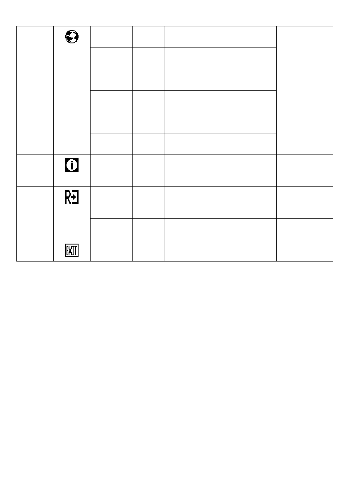
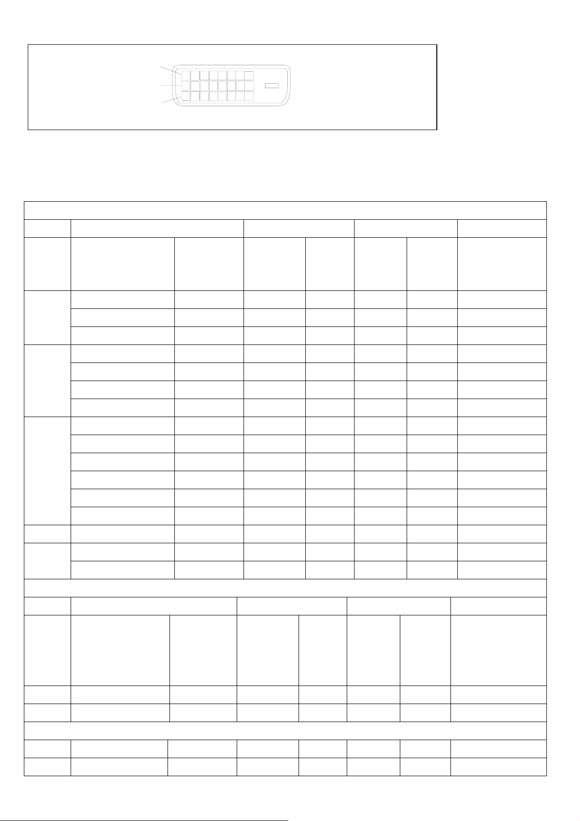
4.1 Input Signal Connector
4.1.1 Analog D-SUB Connector
PIN NO.
1. Red 9. +5V
2. Green 10. Detect Cable
3. Blue 11. NC
4. Ground 12. DDC-Serial Data
5. Ground 13. H-Sync
6. R-Ground 14. V-Sync
7. G-Ground 15. DDC-Serial Clock
8. B-Ground
DESCRIPTION
DESCRIPTION
PI N NO.
VGA connector layout
15
6
11 15
10
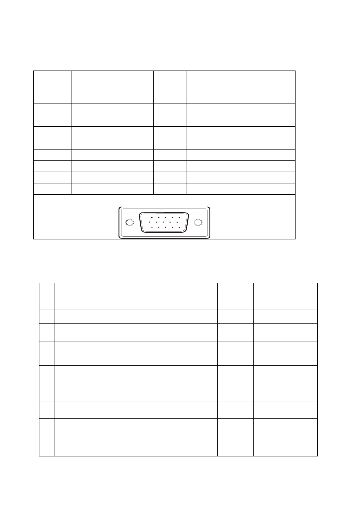
4.1.2 DVI-D Connector
DVI-D Connector to be compliant to the latest DVI-DDWG specification version available.
Pin Meaning Pin Meaning Pin Meaning
TMDS Data2-
1
2 TMDS Data2+ 10
TMDS Data 2/4
3
TMDS Data1-
9
TMDS Data1+
17
18
11 TMDS Data 1/3 Shield 19
TMDS Data0-
TMDS Data0+
TMDS Data 0/5 Shield
Shield
not connected
4
5 not connected 13
12 not connected 20 not connected
not connected
21 not connected
6 DDC Clock 14 +5V Power 22 TMDS Clock Shield
7 DDC Data 15 Ground 23 TMDS Clock-
Analogue Vertical
8
Hot Plug Detect
16
24 TMDS Clock+
Sync
Page 11 of 61
Page 12
LM-729 Service Manual Rev: A
1
9
17
4.2 Factory Preset Display Modes
VESA MODES
Horizontal Vertical
Mode Resolution Total
640x480@60Hz 800 x 525 31.469 N 59.940 N 25.175
VGA
640x480@72Hz 832 x 520 37.861 N 72.809 N 31.500
640x480@75Hz 840 x 500 37.500 N 75.00 N 31.500
800x600@56Hz 1024 x 625 35.156 N/P 56.250 N/P 36.000
800x600@60Hz 1056 x 628 37.879 P 60.317 P 40.000
SVGA
800x600@72Hz 1040 x 666 48.077 P 72.188 P 50.000
800x600@75Hz 1056x625 46.875 P 75.000 P 49.500
1024x768@60Hz 1344x806 48.363 N 60.004 N 65.000
1024x768@60Hz 1312x813 48.78 N 60.00 N 64.000
1024x768@70Hz 1328x806 56.476 N 70.069 N 75.000
XGA
1024x768@72Hz 1304x798 57.515 P 72.074 P 75.000
1024x768@75Hz 1328x804 60.200 N 74.90 N 80.000
1024x768@75Hz 1312x800 60.023 P 75.029 P 78.750
Nominal
Frequency
+/- 0.5kHz
Sync
Polarity
Nominal
Freq.
+/- 1 Hz
Sync
Polarity
Nominal Pixel
Clock
(MHz)
XGA 1152x864@75Hz 1600x900 67.50 P 75.000 P 108.000
1280x1024@60Hz 1688x1066 63.981 P 60.020 P 108.000
SXGA
1280x1024@75Hz 1688x1066 79.976 P 75.025 P 135.000
IBM MODES
Horizontal Vertical
Nominal
Mode Resolution Total
Nominal
Sync
Frequency
Polarity
+/- 0.5kHz
Nominal
Freq.
+/- 1 Hz
Sync
Polarity
Pixel
Clock
(MHz)
DOS* 720x400@70Hz 900 x 449 31.469 N 70.087 P 28.322
DOS** 640x400@70Hz 800 x 449 31.469 N 70.087 P 25.175
MAC MODES
VGA 640x480@67Hz 864x525 35.000 N 66.667 N 30.240
SVGA 832x624@75Hz 1152x667 49.725 N 74.551 N 57.2832
Page 12 of 61
Page 13
LM-729 Service Manual Rev: A
p
4.3 Power Supply Requirements
4.3.1 Input Requirements
PARAMETER RANGE CONDITION
Input AC Voltage 100 to 240VAC RMS Universal input full range
Input Frequency 60Hz @ 100VAC to 50Hz @
240VAC
Input Current Less than 2.0 Amps RMS Input voltage 100 VAC RMS ; 60 Hertz. Parameter
Less than 1.0 Amps RMS Input voltage 220 VAC RMS ; 50 Hertz. Parameter
Input Power Less than 75 Watts
Power factor > 0.5 Input voltage 120 VAC RMS ; 60
Hertz
Inrush Current Less than 30 A peak Input voltage 100 VAC RMS ; 60 Hertz at all
Less than 50 A peak Input voltage 240 VAC RMS ; 50 Hertz at all
Input Fusing Fuse should be located internal to the
adapter, easily accessible when the
cover is removed
Leakage Current Less than 3.5 mA Input voltage 240 Volts RMS ; 50 Hertz
Hi-Pot Primary to secondary 1.5KVAC for 1 Minute(leakage current 10mA)
Prima1ry to Safety Ground 1.5KVAC for 1 Minute(leakage current 10mA)
must be reached within 3 seconds of turn-on.
must be reached within 3 seconds of turn-on.
Phase(0, 90, 180, 270 degree)
Phase(0, 90, 180, 270 degree)
Fuse must be UL/CSA approved. Fuse value must no
have to change for 115 VAC or 230 VAC operation
1.8KVAC for 1 Minute(leakage current 10mA)
3.0KVAC for 1 Minute(leakage current 10mA)
without Y-cap & Coupling cap.
1.8KVAC for 1 Minute(leakage current 10mA)
4.3.2 Output Requirements
PARAMETER RANGE CONDITION
DC Out 12VDC ± 5% Min 0A Max 3.75A
Load Regulation 12.0V(12.12V) ± 5% 11.4 to 12.6VDC
Dynamic Load
Regulation
Ripple & noise 170mVpp at 12VDC Input voltage : 100VAC at 60Hz 240VAC at 50Hz
Output current
rotection
Leakage Current Less than 0.25 mA Input voltage 100 Volts RMS ; 50 Hertz
Less than 0.5 mA Input voltage 240 Volts RMS ; 50 Hertz
Any frequency up to 250Hz(duty
50%)
less than 7.0A, more than 12.0A
at 12.0VDC
±5% for 10% to 100%, 100% to 10% load change for
+12Vdc
* Ripple and noise are measured.
Current exceeds maximum rateing more than 20%
Page 13 of 61
Page 14
LM-729 Service Manual Rev: A
4.4 PANEL SPECIFICATION
4.4.1 Panel Feature
-High contrast ratio, high aperture structure
-TN(Twisted Nematic) mode
-Wide viewing angle
-High speed response
-SXGA(1280 x 1024 pixels) resolution
-Low power consumption
-2 dual CCFTs(Cold Cathode Fluorescent Tube)
-DE(Data Enable) mode
-COMPACT SIZE DESIGN
4.4.2 Display Characteristics
Items Specification Unit
Display Area 337.92(H) x 270.336(V) mm
Driver element a-Si TFT active matrix
Display color 16.2M Colors
Number of pixels 1280 x 1024 pixel
Pixel Arrangement RGB vertical stripe
Pixel pitch 0.264(H) x 0.264(W) mm
Display Mode Normally White
4.4.3 Optical Characteristics
The optical characteristics are measured under stable conditions at 25℃ (Room Temperature):
Item Symbol Conditions Min. Typ. Max. Unit Note
Contrast Ratio
(Center of screen)
Response
Time
Luminance of White
(Center of screen)
Chromaticity
Coordinates (CIE)
Brightness Uniformity [%] 75 80 -
Rising
Falling Tf - 12 20
Color
(CIE 1931)
C/R 250 450 -
Tr
YL 200 260 - Cd/m2
Rx 0.64
Ry 0.34
Gx 0.29
Gy 0.61
Bx 0.14
By 0.07
Wx 0.31
Wy
Normal
ψ=0
θ=0
Viewing
Angle
- 4 5
Typ.
-0.03
0.33
TYP.
+0.03
msec
Page 14 of 61
Page 15
LM-729 Service Manual Rev: A
4.4.4 Parameter guide line for CCFL Inverter
INVERTERMAXBRINGTHNESS(Vadj:5.0v),LOAD=120KΩX4(ROOMTEMPERATURE25℃ ±4℃)
ITEM SYMBOL MIN. TYP. MAX. UNIT REMARK
Inputvoltage Vin 10.8 12 13.2 V
Inputcurrent Iin2250 2500 mA FOR4LOAD
OutputCurrent Iout 6.0 6.5 7.0 mA FOR1LOAD
Frequency
F 50.0 55.0 60.0 KHZ
FOR1LOAD
H.Vopen Vopen 1450 1600 1750 Vrms NOLOAD
H.VLoad Vload 710 810 910 Vrms
Startvoltage Vst
Protectdelaytime PDT
INVERTERMINBRINGTHNESS(Vadj:0.0v),LOAD=120KΩX4(ROOMTEMPERATURE25℃ ±4℃)
1650 1750 1850 Vrms RL=CCFL
0.4 1 4 Sec
RL=120KΩ
ITEM SYMBOL MIN. TYP. MAX. UNIT REMARK
inputvoltage Vin 10.8 12 13.2 V
inputcurrent Iin660 750 mA FOR4LOAD
OutputCurrent Iout 3.0 3.5 4.0 mA FOR1LOAD
Frequency
F 50.0 55.0 60.0 KHZ
FOR1LOAD
H.Vopen Vopen 1450 1600 1750 Vrms NOLOAD
Startvoltage Vst
H.VLoad Vload 350 450 550 Vrms
1650 1750 1850 Vrms RL=CCFL
RL=120KΩ
Page 15 of 61
Page 16
LM-729 Service Manual Rev: A
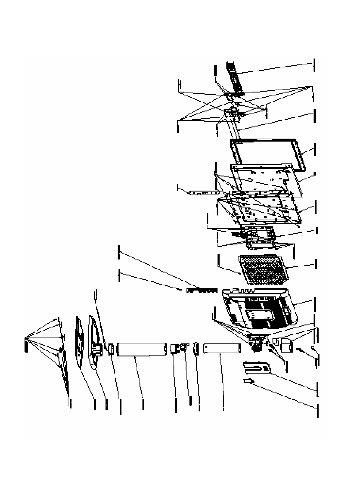
5. Block Diagram
5.1 Monitor Exploded View
Page 16 of 61
Page 17
LM-729 Service Manual Rev: A
2
10
12
643
8
9
141113
1
16
1719
18
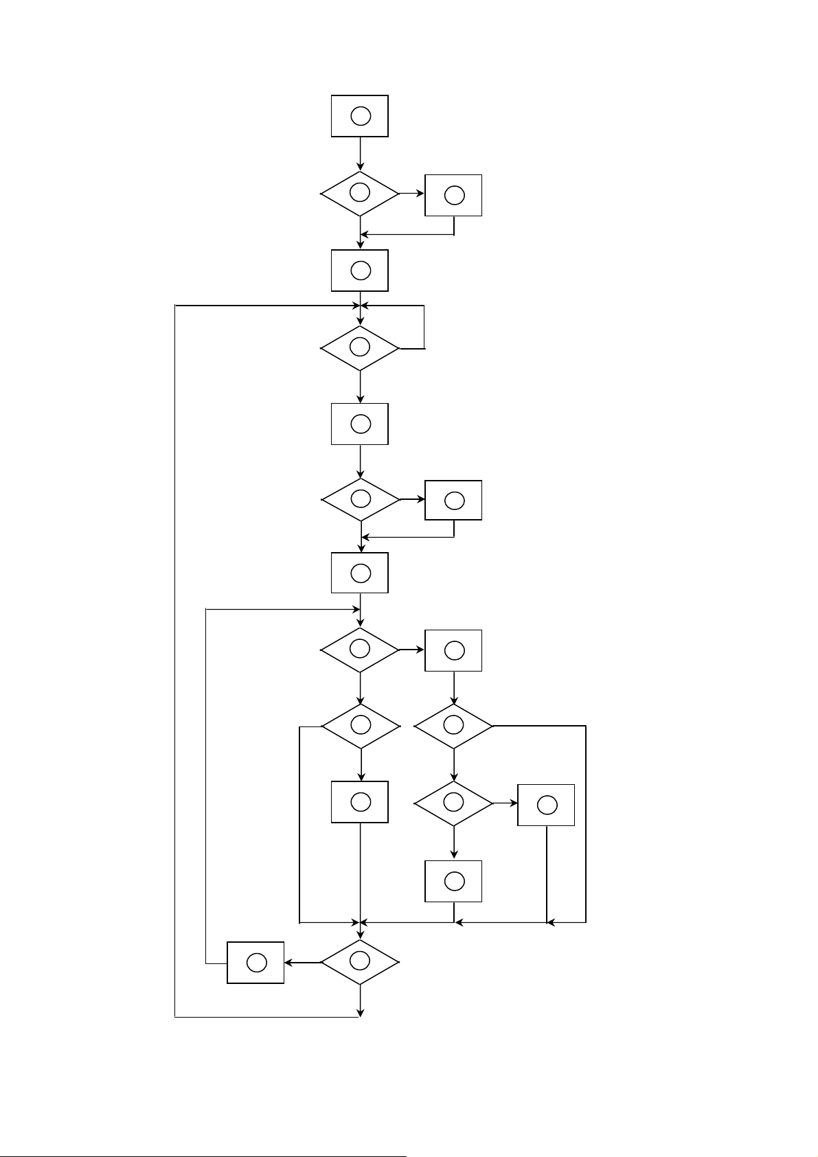
5.2 Software Flow Chart
1
Y
N
N
5
N
Y
7
N
Y
N
Y
N
Y
Y
N
5
Y
N
Y
Page 17 of 61
Page 18

LM-729 Service Manual Rev: A
Remark:
1) MCU initialize.
2) Is the EEprom blank ?
3) Program the EEprom by default values.
4) Get the PWM value of brightness from EEprom.
5) Is the power key pressed ?
6) Clear all global flags.
7) Are the AUTO and SELECT keys pressed ?
8) Enter factory mode.
9) Save the power key status into EEprom.
Turn on the LED and set it to green color.
Scalar initialize.
10) In standby mode ?
1 1 ) Update the life time of back light.
12) Check the analog port, are there any signals coming ?
13) Does the scalar send out a interrupt request ?
14) Wake up the scalar.
15) Are there any signals coming from analog port ?
16) Display "No connection Check Signal Cable" message. And go into standby mode after
the message disappear.
17) Program the scalar to be able to show the coming mode.
18) Process the OSD display.
19) Read the keyboard. Is the power key pressed ?
Page 18 of 61
Page 19
LM-729 Service Manual Rev: A
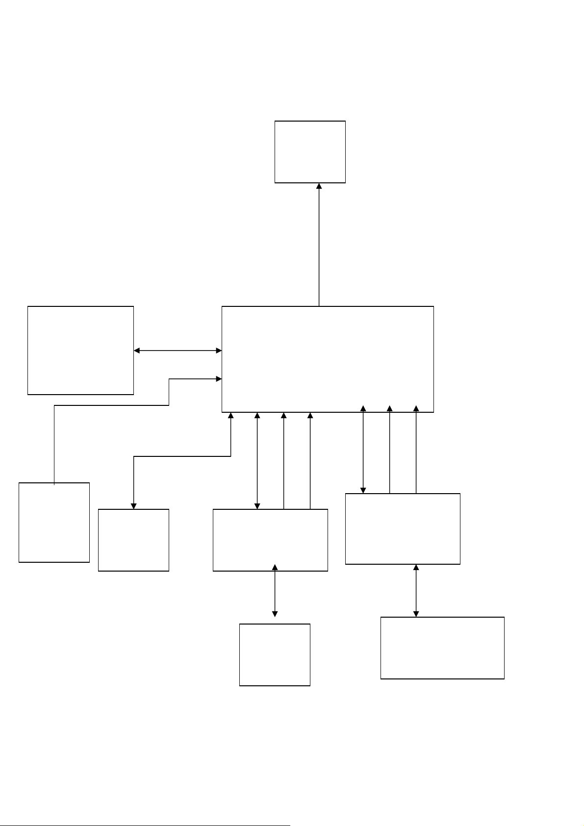
5.3 Electrical Block Diagram
5.3.1 Main Board
LCD
Interface
(CN4/CN5)
Flash Memory
W39f010P-70B
(U6)
OSD
Control
Interface
(CN9)
EPR_SDA
EPR_SCL
EEPROM
24C16
(U7)
RXD
TXD
Connector
DB15_SDA,
DB15_SCL
EEPROM
Scalar gm5126/gm2126
(Include MCU,ADC,OSD)
(U4)
RGB
Hsync,
Vsync
D-Sub
(CN2)
24C02
(U2)
DVI-I only
Connector
(CN1)
EEPROM (D-I only)
24C02
(U1)
Page 19 of 61
Page 20

LM-729 Service Manual Rev: A
5.3.2 Inverter/Power Board
Inverter Block Diagram
Vin
Vin
Buck Connector
Driver
Circuit
Driver
Circuit
Dim ming control
Pa rallet-reso na nt
inv e rter
Dimm ing control
(PW M )
(阀菠瓜)
Parallet-resonant
inverter
CCFL
PW M
Page 20 of 61
Page 21

LM-729 Service Manual Rev: A
Power Block Diagram
PWPC7425A3
Page 21 of 61
Page 22

LM-729 Service Manual Rev: A
6. Schematic
6.1 Main Board
CN1
1
26
A_GND
T2-
2
T2+
3
SGND
4
T4-
5
T4+
R1 47 1/16W
6
DDCCLK
DDCDAT
A_VSYNC
A_GREEN
A_BLUE
A_HSYNC
A_GND
25
A_GND
DVI_5V
C5
0.1uF/16V
GND
U1
81
VCCA0
2
7
A1A2WP
3
6
SCL
4
5
SDA
GND
M24C02WMN6
GND
VGA_5V
2
C12
0.1uF/16V
GND
U2
81
VCCA0
2
7
A1A2WP
3
6
SCL
4
5
SDA
GND
M24C02WMN6
GND
SOT23
3
2
1
SGND
SGND
SGND
A_RED
T1-
T1+
T3T3+
+5V
GND
HPD
T0T0+
T5T5+
TC+
TC-
2
DDC_5V
3
10K 1/16W
3
+5V
1
7
8
9
10
11
12
13
14
15
16
17
18
19
20
21
22
23
24
C1
C2
C3
C4
27
+5V
1
R11
D13
BAT54C-GS08
R20
MLL5232B 5.6V
ZD6
GND
GND
AGND
D9
BAT54C-GS08
R12
10K 1/16W
MLL5232B 5.6V
ZD4
GND
R2 47 1/16W
DVI_5V
HOT_PLUG
R21
10K 1/16W
MLL5232B 5.6V
ZD7
R3 10K 1/16W
10K 1/16W
MLL5232B 5.6V
ZD5
DDC_SDA_A1
DDC_SCL_A1
+5V
C1
0.1uF/16V
1
2
1
2
RX2-IN
RX2+IN
DDC_SCL_D1
DDC_SDA_D1
RX0-IN
RX0+IN
RX1-IN
RX1+IN
RXC+IN
RXC-IN
ZD1
MLL5232B 5.6V
GND
DIGITAL USE
DDC_SCL_D1
R13 NC GND
DDC_SDA_D1
R14 NC
UART_DI
R19 47 1/16W
HSin
VSin
R28
47 1/16W
2K 1/16W
R42
NC
DDC_SCL_D 3
DDC_SDA_D 3
VGA_5V
CN2
1617
DB15
Rin
1
11
12
13
14
15
AGND
R35
2K 1/16W
R43
NC
6
2
7
3
8
4
9
5
10
AGND
GND
Pins 6/7/8 are R/G/B
return lines resp.
R38 47 1/16W
R40 47 1/16W
Gin
Bin
UART_DO
MLL5232B 5.6V
ZD8
C18
NC
AGND
GND
GND
R34
2
2
2
1
2
D11
BAV99
3
R29
75 1/16W
75-ohm terminating resistor
very close to the VGA
conn.
(8 mil)
MLL5232B 5.6V
ZD9
C19
NC
AGND
3
1
3
1
3
1
3
1
2
3
R30
75 1/16W
AGND
GND
D1
D2
BAV99
BAV99
3
+5V
C2
0.1uF/16V
1
2
GND
D3
D4
BAV99
BAV99
3
+5V
C3
0.1uF/16V
1
2
GND
D5
D6
BAV99
BAV99
3
+5V
C4
0.1uF/16V
1
2
GND
D7
D8
BAV99
BAV99
3
+5V
C6
0.1uF/16V
1
2
D10
BAV99
R15
3
R16
R17
R18
R24
R27
R31
75 1/16W
D12
BAV99
100 1/16W
100 1/16W
100 1/16W
100 1/16W
100 1/16W
100 1/16W
1 2
ADC_AGND
U3A
147
74LCX14
FB2 0 1/16W
FB3 0 1/16W
5 6
(10 mil,
┰キ︽絬
FB1 0 1/16W
VGA_CONN
DDC_5V
U3C
147
74LCX14
RX2- 3
RX2+ 3
RX1- 3
RX1+ 3
RX0- 3
RX0+ 3
RXC+ 3
RXC- 3
ADC_AGND
)
R32
4.7K 1/16W
R33
10K 1/16W
AGND
AGND
C7
C8
C9 NC
C10
C11
C13 NC
C14
C15
C16 NC
9 8
AGND
0.01uF/50V
0.01uF/50V
0.01uF/50V
0.01uF/50V
0.01uF/50V
0.01uF/50V
VGA_PLUG
3 4
AGND
147
74LCX14
6/24
U3D
AGND
147
AGND
AGND
U3B
74LCX14
R41
RED+ 3
RED- 3
GREEN+ 3
GREEN- 3
BLUE+ 3
BLUE- 3
VGA_PG 3
R39 0 1/16W
0 1/16W
AGND
DDC_SCL_A1
DDC_SDA_A1
UART_DO
UART_DI
C20
NC
AGND
Connect two grounds at one single point only.
AGND
DVI_5V
R4 NC
R5 100 1/16W
R6 100 1/16W
R8 100 1/ 16W
R10 100 1/16W
MLL5232B 5.6V
MLL5232B 5.6V
ZD2
ZD3
GND
+5V
+3V3
R26
R25
0 1/16W
NC
C17
0.1uF/16V
AGND
U3VCC
VS 3
HS 3
C21
NC
AOC
Title
ANALOG&DIGITAL INPUT
Size Document Number Rev
gm5126 A
C
星期二, 七月
Date: Sheet of
22, 2003
DVI_PLUG 3
DDC_SCL_A 3
DDC_SDA_A 3
GND
GPIO5UART_DO
GPIO4UART_DI 3
3
28
Page 22 of 61
Page 23

LM-729 Service Manual Rev: A
3V3_DDDS
C24
0.1uF/16V
GND
RVSS
77
GND
173
AVDD_RPLL
RVSS
102
179
+3V3
169
167
164
162
VDD_SDDS
VDD_DDDS
AVDD_SDDS
AVDD_DDDS
RVSS
RVSS
EAVSS_RS
EAVSS_RS
AVSS_RS
OAVSS_RS
OAVSS_RS
199142638486085
FB18
600 OHM
C27
C28
GND
Close to respective power Pins
158
76
171
VDD_DPLL
36
160
101
198
13253747593584
115
121
127
178
RVDD
RVDD
RVDD
RVDD
VDD_RX2_2.5
VDD_RX1_2.5
VDD_RX0_2.5
EAVDD_RS_2.5
EAVDD_RS_2.5
VDD1_ADC_2.5
VDD2_ADC_2.5
GPIO10/TCON_ROE3
GPIO9/TCON_ROE2
GPIO21/TCON_FSYNC
GPIO12/NVRAM_SDA
GPIO13/NVRAM_SCL
GPIO6/TCON_SHC
GPIO7/TCON_TDIV
GPIO5/UART_DO
CVSS
CVSS
CVSS
GND1_ADC
GND2_ADC
GND_RX2
GND_RX1
CVSS
GND_RX0
111
186
157
159
116
122
128
170
AVDD_RS
OAVDD_RS_2.5
OAVDD_RS_2.5
OCH11P_RS
OCH11N_RS
OCH10P_RS
OCH10N_RS
OCH9P_RS
OCH9N_RS
OCH8P_RS
OCH8N_RS
OCH7P_RS
OCH7N_RS
OCH6P_RS
OCH6N_RS
OCH5P_RS
OCH5N_RS
OCH4P_RS
OCH4N_RS
OCLKP_RS
OCLKN_RS
OCH3P_RS
OCH3N_RS
OCH2P_RS
OCH2N_RS
OCH1P_RS
OCH1N_RS
OCH0P_RS
OCH0N_RS
ECH11P_RS
ECH11N_RS
ECH10P_RS
ECH10N_RS
ECH9P_RS
ECH9N_RS
ECH8P_RS
ECH8N_RS
ECH7P_RS
ECH7N_RS
ECH6P_RS
ECH6N_RS
ECH5P_RS
ECH5N_RS
ECH4P_RS
ECH4N_RS
ECLKP_RS
ECLKN_RS
ECH3P_RS
ECH3N_RS
ECH2P_RS
ECH2N_RS
ECH1P_RS
ECH1N_RS
ECH0P_RS
ECH0N_RS
TCON_OSP
TCON_OPOL
TCON_OINV
TCON_RSP2
TCON_RSP3
TCON_RCLK
TCON_ROE
TCON_ESP
TCON_EINV
TCON_EPOL
DHS/TCON_LP
GPIO8/IRQINn
GPIO0/PWM0
GPIO1/PWM1
GPIO2/PWM2
GPIO3/TIMER1
GPIO4/UART_DI
VSS_DPLL
VSS_DDDS
VSS_SDDS
166
161
R53
R220
NC
NC
NAME
USER_BITS(4:0)
Reserved
SCLPOL
HOST_PROTOCOL
HOST_PORT_EN
OCM_START
USER_BITS(7:5)
OSC_SEL
OCM_ROM_CFG(1)
R221
NC
10K 1/16W
BOOTSTRAP SIGNALS
ADDRESS
ROM_ADDR(4:0)
ROM_ADDR5 x
ROM_ADDR6
ROM_ADDR7
ROM_ADDR8
ROM_ADDR9
ROM_ADDR(12:10)
ROM_ADDR13
ROM_ADDR14
+3V3
+5V
+3V3
R49
R50
NC
0 1/16W
+PV
+PV
R65
R64
R61
R60
R63
R62
R67
R222
NC
NC
NC
SET
x
Available for reading from a status register
If using 6-wire host protocol, program this bit to 0
Determines polarity of HCLK signal
x
If using 6-wire host protocol, program this bit to 1
0
GPIO(22:16) is on "Host Port" pins
1
1
1 = OCM becomes active after OCM_CLK is stable
x
Available for reading from a status register
0 = XTAL and TCLK pins are connected
0
1 = All 48K of ROM is in external ROM
1
NC
NC
10K 1/16W
10K 1/16W
DESCRIPTION
R46
4.7K 1/16W
U5 TCM809SENB713/NC
VCC
1
GND
ROM_WE
BANK1
R66
BANK0
10K 1/16W
RMADDR14
RMADDR9
RMADDR8
RMADDR10
RMADDR11
RMADDR3
RMADDR4
RMADDR12
RMADDR2
RMADDR1
RMADDR0
C48
22uF/16V
+3V3
+
GND
RST
10K 1/16W
+3V3
GND
C70
22uF/16V
23
R56
+
+PV
+3V3
D14
LL4148
Reset
Circuit
DIGITAL PORT
ROMCE
FB7
600 OHM
R48
NC
R57
10K 1/16W
R59
0 1/16W
RMADDR15
RMADDR14
RMADDR13
RMADDR12
RMADDR11
RMADDR10
RMADDR9
RMADDR8
RMADDR7
RMADDR6
RMADDR5
RMADDR4
RMADDR3
RMADDR2
RMADDR1
RMADDR0
22uF/16V
FB8
600 OHM
+PV
+
C49
GND
C57
22uF/16V
CTRLP12V4
DDC_SDA_A2
DDC_SCL_A2
DDC_SDA_D2
R218
NC
R219
0 1/16W
GND
C50
C51
0.1uF/16V
0.1uF/16V
+
C58
0.1uF/16V
GND
PPWR4
PBIAS7
STDBY7
VGA_PG2
DDC_SCL_D2
RED+2
RED-2
GREEN+2
GREEN-2
BLUE+2
BLUE-2
HS2
VS2
RXC+2
RXC-2
RX2+2
RX2-2
RX1+2
RX1-2
RX0+2
RX0-2
U6
31
WE
30
NC/A17
2
A16
3
A15
29
DQ7
A14
28
DQ6
A13
4
DQ5
A12
25
DQ4
A11
23
DQ3
A10
26
DQ2
A9
27
DQ1
A8
5
DQ0
A7
6
A6
7
A5
8
A4
9
A3
10
A2
11
A1
12
A0
24
OE
VCC
22
GND
CE
W39F010P
R225
10K 1/16W
32-Pin PLCC Socket
FLASH/ Prom-Jet Socket
ROMCE
BANK1
NC
+2V5
C52
0.1uF/16V
C59
0.1uF/16V
+3V3
C69
5pF/50V
21
20
19
18
17
15
14
13
1
32
16
FB9
600 OHM
C68
5pF/50V
RMDATA1
RMDATA0
+3V3
+3V3
RMDATA7
RMDATA6
RMDATA5
RMDATA4
RMDATA3
RMDATA2
+PV
GND
FB4
600 OHM
FB6
600 OHM
3V3_RGB
C53
0.1uF/16V
3V3_DVI
C60
0.1uF/16V
C64
22uF/16V
X1
14.318MHz
12
R223 0 1/16W
R224 NC
R217 NC
RESET
FB10
600 OHM
C71
0.1uF/16V
0.1uF/16V
C61
0.1uF/16V
GND
C66
C54
+
0.1uF/16V
NC
C35
22uF/16V
AGND
C65
R47
NC
+3V3
C25
0.1uF/16V
GND
GND
C55
0.1uF/16V
C62
0.1uF/16V
GND
GND
TCLK
RMADDR15
RMADDR14
RMADDR13
RMADDR12
RMADDR11
RMADDR10
RMADDR9
RMADDR8
RMADDR7
RMADDR6
RMADDR5
RMADDR4
RMADDR3
RMADDR2
RMADDR1
RMADDR0
RMDATA6
RMDATA5
RMDATA4
RMDATA3
RMDATA2
RMDATA1
RMDATA0
ROM_OEn
C23
22uF/16V
+
0.1uF/16V
GND
AGND
C67
AGND
NC
XTAL
BANK0
ROM_WE
R51 1K 1/16W
+3V3
GND
C37
+
3V3_SDDS
153
149
145
141
156
155
152
148
144
135
132
126
120
112
136
129
123
117
114
138
172
168
163
137
78
79
175
174
90
91
92
93
89
88
108
109
107
81
150
151
146
147
142
143
176
177
154
133
134
118
119
124
125
130
131
113
180
181
182
183
184
187
188
189
190
191
192
193
194
195
196
197
200
201
202
203
204
205
206
207
208
FB5
600 OHM
U4
GM5126
AVDD_ADC
AVDD_RED
AVDD_GREEN
AVDD_BLUE
SGND_ADC
AGND_ADC
AGND_RED
AGND_GREEN
AGND_BLUE
AVDD_RXC
AVDD_RX0
AVDD_RX1
AVDD_RX2
AVDD_IMB
AGND_RXC
AGND_RX0
AGND_RX1
AGND_RX2
AGND_IMB
VDD_RXPLL_2.5
AVSS_RPLL
AVSS_DDDS
AVSS_SDDS
GND_RXPLL
PPWR
PBIAS
TCLK
XTAL
GPIO20/HDATA3
GPIO19/HDATA2
GPIO18/HDATA1
GPIO17/HDATA0
GPIO16/HFS
GPIO22/HCLK
GPIO14/DDC_SCL
GPIO15/DDC_SDA
RESETn
GPIO11/ROM_WEn
RED+
REDGREEN+
GREENBLUE+
BLUEHSYNC
VSYNC
ADC_TEST
RXC+
RXCRX2+
RX2RX1+
RX1RX0+
RX0-
REXT
ROM_ADDR15
ROM_ADDR14
ROM_ADDR13
ROM_ADDR12
ROM_ADDR11
ROM_ADDR10
ROM_ADDR9
ROM_ADDR8
ROM_ADDR7
ROM_ADDR6
ROM_ADDR5
ROM_ADDR4
ROM_ADDR3
ROM_ADDR2
ROM_ADDR1
ROM_ADDR0
ROM_DATA7
ROM_DATA6
ROM_DATA5
ROM_DATA4
ROM_DATA3
ROM_DATA2
ROM_DATA1
ROM_DATA0
ROM_OEn
C29
110
CVDD_2.5
CVDD_2.5
Reserved
Reserved
CLKOUT
+2V5
C33
C30
FB19
600 OHM
+
C47
C36
185
22uF/16V
GND
CVDD_2.5
CVDD_2.5
68
67
66
65
64
63
62
61
58
57
56
55
54
53
52
51
50
49
46
45
44
43
42
41
40
39
34
33
32
31
30
29
28
27
24
23
22
21
20
19
18
17
16
15
12
11
10
9
8
7
6
5
69
71
70
72
73
R89 33 1/16W
74
75
1
2
3
4
80
105
106
SDA
82
SCL
83
94
GPIO0/PWM0
95
96
GPIO2
97
GPIO3
98
GPIO6
103
GPIO7
104
99
100
86
87
139
N/C
165
GND
N/C
140
C31
C34
0.1uF/16V
0.1uF/16V
GND
Close to respective power Pins
C38
C39
0.1uF/16V
0.1uF/16V
ADD DEN SIGNAL PIN 4/28
OD22P
OD22N
OD21P
OD21N
OD20P
OD20N
OD12P
OD12N
OD11P
OD11N
OD10P
OD10N
OCLK_RS_P
OCLK_RS_N
OD02P
OD02N
OD01P
OD01N
OD00P
OD00N
ED22P
ED22N
ED21P
ED21N
ED20P
ED20N
ED12P
ED12N
ED11P
ED11N
ED10P
ED10N
ECLK_RS_P
ECLK_RS_N
ED02P
ED02N
ED01P
ED01N
ED00P
ED00N
R87 33 1/16W
R88 33 1/16W
R92 33 1/16W
R52 22 1/16W
R54 22 1/16W
R55 22 1/16W
DVI_PLUG
+3V3
+5V
R68
NC
R70
R71
10K 1/16W
10K 1/16W
SCL
SDA
GND
Title
Size Document Number Rev
C
Date: Sheet
C32
0.1uF/16V
0.1uF/16V
C45
A0
A1
A2
VSSSI
C42
0.1uF/16V
2
1
2
3
45
C43
0.1uF/16V
TCON_OSP 4
TCON_RSP2 4
TCON_RCLK 4
TCON_ROE 4
TCON_ESP 4
TCON_EPOL 4
TCON_LP 4
22pF/NC
GND
GND
0.1uF/16V
C79
C44
0.1uF/16V
C74
22pF/NC
GND
C40
0.1uF/16V
OD22P 4
OD22N 4
OD21P 4
OD21N 4
OD20P 4
OD20N 4
OD12P 4
OD12N 4
OD11P 4
OD11N 4
OD10P 4
OD10N 4
OCLK_RS_P 4
OCLK_RS_N 4
OD02P 4
OD02N 4
OD01P 4
OD01N 4
OD00P 4
OD00N 4
ED22P 4
ED22N 4
ED21P 4
ED21N 4
ED20P 4
ED20N 4
ED12P 4
ED12N 4
ED11P 4
ED11N 4
ED10P 4
ED10N 4
ECLK_RS_P 4
ECLK_RS_N 4
ED02P 4
ED02N 4
ED01P 4
ED01N 4
ED00P 4
ED00N 4
TCON_OSP
TCON_RSP2
TCON_RCLK
TCON_ROE
TCON_ESP
TCON_EPOL
TCON_LP
LED_ORANGE 5
LED_GRN 5
DVI_PLUG 2
GPIO8 5
PWM0 7
VOLUME 7
GPIO2 5
GPIO3 5
GPIO6 5
GPIO7 5
GPIO4UART_DI
GPIO5UART_DO 2
R69
0 1/16W
C72
0.1uF/16V
8
VCC
7
WP
6
SCK
M24C16-MN6T
C41
0.1uF/16V
U7
AOC
gm5126
gm5126 A
星期二, 七月
22, 2003
38
of
C46
0.1uF/16V
GND
C86
22pF/NC
GND
C76
22pF/NC
0.1uF/16V
Page 23 of 61
Page 24

LM-729 Service Manual Rev: A
+P5V
+
C73
100uF/16V
+P3V3
+
C75
100uF/16V
GND
TCON_ROE3
TCON_RSP23
R76
TCON_OSP3
0 1/16W
R77
NC
GND
TCON_RCLK3
TCON_EPOL3
TCON_LP3
TCON_ESP3
ED00N3
ED00P3
ED01N3
ED01P3
ED02N3
ED02P3
ECLK_RS_N3
ECLK_RS_P3
ED10N3
ED10P3
ED11N3
ED11P3
ED12N3
ED12P3
ED20N3
ED20P3
ED21N3
ED21P3
ED22N3
ED22P3
GND
R74
TCON_ROE
TCON_RSP2
TCON_RCLK
TCON_EPOL
TCON_LP
TCON_ESP
ED00N
ED00P
ED01N
ED01P
ED02N
ED02P
ECLK_RS_N
ECLK_RS_P
ED10N
ED10P
ED11N
ED11P
ED12N
ED12P
ED20N
ED20P
ED21N
ED21P
ED22N
ED22P
R72
0 1/16W
NC
GND
CONNECTOR for PANEL
R73
0 1/16W
CN4
1
2
3
4
5
6
7
8
9
10
11
12
13
14
15
16
17
18
19
20
21
22
23
24
25
26
27
28
29
30
31
32
33
34
35
36
37
38
39
40
41
42
43
44
45
46
47
48
49
50
CONNECTOR 50P
C200
22uF/16V
R202
NC
R203
100K 1/16W
R84
10K
C78
150uF/16V
C205
150uF/16V
R80
100K 1/16W
1
+
GND
GND
+12V
32
GND
GND
CN5
1
2
3
4
5
6
7
8
9
10
11
12
13
14
15
16
17
18
19
20
21
22
23
24
25
26
27
28
29
30
CONNECTOR 30P
OD00N
OD00N3
OD00P
OD00P3
OD01N
OD01N3
OD01P
OD01P3
OD02N
OD02N3
OD02P
OD02P3
OCLK_RS_N3
OCLK_RS_P3
OCLK_RS_N
OCLK_RS_P
OD10N
OD10N3
OD10P
OD10P3
OD11N
OD11N3
OD11P
OD11P3
OD12N
OD12N3
OD12P
OD12P3
OD20N
OD20N3
OD20P
OD20P3
OD21N
OD21N3
OD21P
OD21P3
OD22N
OD22N3
OD22P
OD22P3
CTRLP12V3
PPWR3
PPWR3
+
1
+
R82
100K 1/16W
Q1
PMBS3904
+12V
100K 1/16W
510K 1/16W
32
GND
C80
0.1uF/16V
R200
R201
Q5
PMBS3904
+P3V3
GND
GND
FB11
R81
C77
100pF
NC
3K 1/16W
+12V
+5V
R78
R75
NC
0 1/16W
R79
NC
R83
FB12
220 OHM
+3V3
NC
+P5V
C82
0.1uF/16V
GND
NC
123
4
Q2
S1G1S2
G2
SI9933ADY-T1
D1D1D2
D2
876
5
R86
R85
3K 1/16W
GND
GND
AOC
Title
Panel Interface(RSDS)
Size Document Number Rev
gm5126 A
B
星期二, 七月
Date: Sheet of
22, 2003
48
Page 24 of 61
Page 25

LM-729 Service Manual Rev: A
+5V
+5V
C111
100uF/16V
GND
0.1uF/16V
+
0.1uF/16V
C125
C110
GND
3
VIN
1
ADJ
AIC1084-33CE
3
VIN
1
ADJ
AIC1084-33CE
C124
0.1uF/16V
C119
0.1uF/16V
+3V3
GND
+2V5
GND
+
+
C126
100uF/16V
C120
100uF/16V
3
PBIAS
PWM0
R113
4.7K
100uF/16V
+5V
R115
4.7K
PWM0
Brightness
C117
3
VOLUME
+12V
+
0.1uF/16V
Brightness
R117
1K
+5V
C121
BackLight
On/Off
GND
GND
FB15
600 OHM
FB16
600 OHM
CN11
2
4
6
8
10
12
GND
PIN HEADER 2*6P
CONNECTOR for
POWER/INVERTER
Board
C127
+
22uF/16V
U8
2
VOUT
R116
1K 1/16W
R118
1.5K 1/16W
GND
U9
2
VOUT
R112
1K 1/16W
R114
1K 1/16W
GND
FB17
600 OHM
1
3
5
7
9
11
+12V
GND
CN601
6P PLUG R/A
12345
+5V
6
Standby
GND
Mute
+
1uF/16V
GND
+
GND
R232
10K 1/16W
C231
R230 10K 1/16W
C230
1uF/16V
D20
LL4148
R231
10K 1/16W
D21
LL4148
STDBY 3
AOC
Title
Power
Size Document Number Rev
gm5126 A
B
星期二, 七月
Date: Sheet of
22, 2003
78
Page 25 of 61
Page 26

LM-729 Service Manual Rev: A
6.2 AUDIO Board
OUT_L
OUT_R
CN204
1
2
3
33L8022-3A-H FEMALE
GND
R201
R203
100 pF
10K 1/4W
10K 1/4W
C211
+12V
14
12
10
8
6
4
2
INL
INR
VOLUME
STBY
MUTE
123
12V
MUTE
8
GND
NC
GND
16
GND
13
GND
15
VS
VS
VAROUT_R
VAROUT_L
GND
GND
GND
181920
CN202
WAFER 2*7P 2.54mm
13
11
9
7
5
3
1
C209
1.0uF
GND
C204 0.47uF
C206 0.47uF
C210
+
1.0uF
GND
STANDBY
C213
0.1uF
4
9
6
11
12
VOLUME
R211
R210
5.6K 1/4W
5.6K 1/4W
GND
220K 1/4W
C212
100 pF
R212
+
FB200
BEAD
+
C201
470uF/16V
U201 TDA7496L!
17
OUTL
14
OUTR
10
SVR
7
5
GND
C208
470uF/16V
GND
+
C202
470uF/16V
+
R207
1K 1/4W
GND
C203
0.1uF
C205
+
470uF/16V
+
C207
470uF/16V
R208
1K 1/4W
C215
1000 pF
C214
1000 pF
WAFER 4P2.0 R/A
GND
4
3
2
1
CN203
Title
Title
Size Document Number Rev
A
Audio
Size Document Number Rev
Date: Sheet of
<Doc> <RevCode>
A
Date: Sheet of
Page 26 of 61
<Title>
<Doc> <RevCode>
11
11
星期三, 五月
星期三, 五月
21, 2003
21, 2003
Page 27

LM-729 Service Manual Rev: A
4
6.3 Key Board
1
U3E
LED_ORANGE3
LED_GRN3
11 10
74LCX14
7
147
13 12
74LCX14
U3F
C83
GND
0.001uF
1
8
7
6
5
SOT-23
3
2
10K 1/16W
KEY_LEFT
KEY_AUTO
KEY_MENU
KEY_RIGHT
KEY_ONOFF
C
E
B
+3V3
123
876
4
RP2
10K 1/16W
5
AOC
Title
Keypad
Size Document Number Rev
gm5126 A
B
星期二, 七月
Date: Sheet of
22, 2003
58
R94
R90
0 1/16W
LED_GRN
KEY_AUTO
KEY_RIGHT
KEY_ONOFF
C84
C85
C88
0.001uF
0.001uF
0.001uF
CN9
2
1
4
3
6
5
8
7
WAFER 8P2.0 DUAL R/A
LED_GRN
LED_ORG
KEY_MENU
KEY_LEFT
GND
R91
LED_ORG
0 1/16W
C96
0.001uF
RP3
GPIO63
C97
C98
0.001uF
0.001uF
GPIO83
GPIO33
GPIO73
GPIO23
1
2
3
4
4.7K 1/16W
R95 4.7K 1/16W
Page 27 of 61
Page 28

LM-729 Service Manual Rev: A
6.4 Inverter/Power Board
C920
R920
0.001uF/500V
4
2KBP06M
1
-+
2
2 3
L902
1 4
C904 0.47uF/250V
2 3
L901
1 4
C903 0.1uF/250V
R901
R902
1M 1/16W
1M 1/16W
C902
C901
0.001uF/250V
0.001uF/250V
3
12
CN901
DB901
47 1/ 2W
T901
1
O
R906
+
D904
1N4148
D905
1N4148
P901A
1
2
Wire Harness
C905
120uF/400V
R909
4.7K 1/16W
ZD901
RLZ20B
R912
100 1/ 16W
R916
24K 1/ 10W
3
NR901
NTCR
t
F901
FUSE
1M 1/4W
R907
1M 1/4W
C908
0.1uF
IC901
72
8
4
SG6841
56
13
R915
10K 1/ 16W
R914
N.C/0603
Q901
2PA733P
C910
0.1uF
C911
0.001uF
0.1uF
R911
4.7K 1/16W
R913
N.C_0603
SG6841
C909
R904
1M 1/4W
R905
1M 1/4W
C907
10uF
R917
JUMPER
C912
N.C
C906
0.0015uF/2KV
+
PS102R
12
R918
20K 1/ 4W
R910
4.7K 1/16W
Q902
2PC945P
D902
R903
100K 2W
D901
UF4007
Q903
2SK2996
FB901
BEAD
R919
0.39 2W
D903
1N4148
R908
10 1/ 4W
3
5
O
4
C913
0.0022uF/250V
43
IC903
HTL431
9
O
7,8
7,8
10,11
12
PC123FY2 4P
IC902
R922
47 1/ 4W
C936
0.1uF
D910
0.001uF/500V
D912
R930
100 1/ 4W
R931
1K 1/ 16W
12
C921
ZD902
HZ12B2
JUMPER
C935
0.01uF
R929
+
+
R927
1K 1/ 4W
R928
1K 1/ 4W
L903
C922
1000uF/16V
L904
C925
1000uF/16V
ZD903
HZ5C1
R924
33K 1/ 4W
R926
2.4K 1/4W
+
C924
470uF/16V
+
C926
470uF/16V
F902
0 1/ 16W
R925
3.6K 1/4W
FB903
0 1/ 16W
C928
FB902
C927
0.1uF
0.1uF
ZD904
SML4736
<Title>
<OrgName>
Size Document Number Rev
B
PWPC7425B3
Date: Sheet
CON102
12V
12
11
GND
10
9
8
7
GND
6
GND
5
5V
4
5V
3
DIM
2
ON/OFF
1
1
of
12
Page 28 of 61
Page 29

LM-729 Service Manual Rev: A
+12V
+
+
NO/OFF
C201
150uF/25V
R201
30K
DIM
C203
1uF/25V
+
R207
C207
OPEN
10uF
C223
150uF/25V
C202
0.1uF/25V
R202
10K
C205
0.1uF
C206
0.1uF
R206
47K
C208
330pF
R203
10K
R205
47K
SCP
REF
CTRT1IN+
1234567
R204
10K
AOC (Top Victory) Electronics Co., Ltd.
Title
Size Document Number Rev
B
Friday, July 25, 2003
Date: Sheet
22
A
of
R208
4.7K 1/16W
C209
1uF/25V
2IN-
2IN+
2FBK
1IN-
1FBK
C210
1uF/25V
R209
4.7K 1/16W
R211
15K
Q202
DTA144WKA
Q201
DTC144WKA
R210
15K
10111213141516
C204
0.1uF
2OUT
2DTC
U201
1DTC
1OUT
GND Vcc
TL1451ACNSR
8 9
is power GND
is signal GND
1uF/25V
R219
470
C224
1uF/25V
R218
470
C225
R214
3.9K 1/16W
1
R215
3.9K 1/16W
1
Q205
MPS3904
Q207
MPS3906
3 2
Q206
MPS3904
Q208
MPS3906
3 2
R212
3.9K
R213
3.9K
Q203 SI4431DY-T1
1
2
3
4
R216
220 1/16W
Q204 SI4431DY-T1
1
2
3
4
R217
220 1/16W
8
7
6
5
C211
1uF/25V
8
7
6
5
C212
1uF/25V
D201
SR24
D202
SR24
L201
L202
D203
RLZ11B
R220
15K
R222
12K
D204
RLZ11B
R221
15K
R223
12K
R224
2K
Q209
2SC5706
1
R228
2K
Q211
2SC5706
1
R225
2K
C213
0.22uF/100V
23
R229
2K
C214
0.22uF/100V
23
R240
51K
C221
0.47uF/63V
C222
0.47uF/63V
R226
2K 1/16W
Q210
23
2SC5706
R230
2K
Q212
23
2SC5706
R241
51K
1
1
R238
12K
2K 1/16W
D207
1N4148
R231
2K
R227
POWER X'FMR
POWER X'FMR
D208
1N4148
R239
12K
5 9
3,4
2
6
5 9
3,4
2
6
PT201
PT202
71
C219
1uF/25V
71
C220
1uF/25V
C215
22pF/3KV
C216
22pF/3KV
R232
1K
C217
22pF/3KV
C218
22pF/3KV
R233
1K
R236
620
R237
620
D209
1N4148
R234
910 1/4W
D210
1N4148
R235
910 1/4W
D205
1N4148
D206
1N4148
1
2
3
4
CN201
1
2
3
4
CN202
Page 29 of 61
Page 30

Page 31

LM-729 Service Manual Rev: A
7. PCB Layout
7.1 Main Board
Page 31 of 61
Page 32

LM-729 Service Manual Rev: A
Page 32 of 61
Page 33

LM-729 Service Manual Rev: A
7.2 Inverter/Power Board
Page 33 of 61
Page 34

LM-729 Service Manual Rev: A
7.3 Keypad Board and Audio board
1. Keypad Board
Page 34 of 61
Page 35

LM-729 Service Manual Rev: A
2.Audio Board
Page 35 of 61
Page 36

LM-729 Service Manual Rev: A
8. Maintainability
8.1 Equipments and Tools Requirement
1.) Voltmeter .
2.) Oscilloscope.
1.) Pattern Generator.
2.) DDC Tool with a IBM Compatible Computer.
3.) Alignment Tool.
4.) LCD Color Analyzer.
5.) Service Manual.
6.) User Manual.
Page 36 of 61
Page 37

LM-729 Service Manual Rev: A
8.2 Trouble Shooting
8.2.1 Main Board
1.NO SCREEN APPEAR
Measured CN11 pin5 = 12 V?
Measured CN11 pin 9/ 1 0= 5V ?
Measured U8 pin 2= 3.3V?
Check Correspondent component.
Is there any shortage or cold solder?
Measured U9 pin 2= 2.5V?
Yes, all DC level exist
Disconnected the Signal cable( Loose the
Signal cable ),Is the screen show “Cable Not
Connected” ?
No, nothing is show
Connected the Signal cable again,
Check LED status.
Led Green
Check the Wire-Harness from CN2
Led Orange
OK,Wire tight enough
Yes. there have OSD show
Connected the Signal cable again,
Check LED status.
Check Power switch is in Power-on
status , and check if Power switch had
been stuck ?
OK, Keyboard no stuck
Measured RGB (R15,R17,R24) H,V Input at
U4 pin 176,177 ,was there have signal ?
Check digital signal from CN1
Led orange
NG
Led Green
Replace U6
Flash Rom
Check Correspondent
component short/open
( Protection Diode )
Check Panel-Power Circuit Block
OK,Panel Power OK
OK,input Normal
Check U4 Data-output Block
Replace Power board and Check
Inverter control relative circuit
OK, U4 data OK
Measured Crystal X1(14.318MHz)
OK,clock
Replace U203 (GM5126/2126)
Re-do White balance adjust
OK
Note: 1. if Replace “MAIN-BOARD” , Please re-do “DDC-content” programmed & “WHITE-Balance”.
2. if Replace “Power Board” only, Please re-do “ WHITE-Balance”
Page 37 of 61
Page 38

LM-729 Service Manual Rev: A
,
3
2.PANEL-POWER CIRCUIT
check R203 should have response from 0V to 5V
When we switch the power switch from on to off
OK, R86 have response
Measured the Q302 pin 7,8= 5 V?
OK
OK
3.INVERTER Control Relative Circuit
NG
Check the PPWR panel power relative circuit,
Q5, Q2(pin7,8)
In normal operation, when LED =green, R203
should =0 v
NG, no Voltage
Replace Q302 ( N-MOS, SI99
Measured the inverter connector CN11
pin 2 on/off control= 5 V (on)
pin4 PWM signal control dim 0V-5V
NG, still no screen
Replace Power board to new-one, and
Check the screen is normal ??
OK
NG
NG
Check the Bklt-On relative circuit, R113, R115, R117,
In normal operation, when LED =green,
R405 Bklt-On should =5 v,
If Bklt-On no-response when the power switch turn on-off,
Replace U4 GM5126/2126
Replace Power board
& Re-do white balance
Page 38 of 61
Page 39

LM-729 Service Manual Rev: A
–
4.U4-DATA OUTPUT
Measured DCLK(pin 15 or pin 16 from U4)
DVS, DHS (pin 1,4 from U4 )
Is the waveform ok?
DCLK around 48 MHZ , DVS=60.09Hz , DHS
around 80 KHz ?(refer to input
signal=640x480@60 Hz 31k, and LED is
Green)
NG , no transition
Replace GM5126 /2126 (U4) or
replace MAINBOARD.
Check U4 GM5126/2126
Signal output
(PIN17-22,27-32,39-44,51-56,61-66)
Is the waveform ok ?
OK
If MainBoard being replace , please
do the DDC
content reprogrammed
OK
OK
Page 39 of 61
Page 40

LM-729 Service Manual Rev: A
Check R919
910,D911,D912,D913
904
8.2.2 Power/Inverter Board
1.) No power
Check to CN102 Pin1 and
pin2 = 5V
Check Interface board
OK
NG
Check AC line volt 120V or
220V
Check the voltage of C905(+)
Check start voltage for the pin3 of IC901
Check the auxiliary voltage is smaller than 20V
OK
OK
Repeating the start voltage
NG
Change F901 , check BD901,Q903,IC901
NG
Check bridge rectified circuit
NG
Change IC901
NG
1) Check IC902, IC903
, D
2) Check Q901,Q902…OVP circuit
OK
, ZD
Page 40 of 61
Page 41

LM-729 Service Manual Rev: A
2.) W / LED , No Backlight
Check C201(+) =12V
NG
OK
Check ON/OFF signal
NG
OK
Check U201 pin9=12V
NG
OK
Check the pin1 of U201 have sawtooth wave
NG
OK
Change F902
Check D201/Q209/Q210 or
D202/Q211/Q212
Check Interface board
Change Q201 or Q202
Change U201
Check D201(-),D202(-) have the output of square wave at short time.
NG
OK
Check the resonant wave of pin2 & pin5 for PT201/PT202
NG
OK
Check the output of PT201/PT202
NG
OK
Check connecter & lamp
Check Q205/Q207/Q203/D201 or
Q206/Q208/Q204/D202
Check Q209/Q210/C213 or
Q211/Q212/C214
Change PT201or PT202
Page 41 of 61
Page 42

LM-729 Service Manual Rev: A
8.2.3 KeyPad Board
OSD is unstable or not working
Is KeyPad Board connecting normally ?
N
Connect KeyPad Board
Y
N
Is Button Switch normally ?
Replace Button Switch
Y
N
Is KeyPad Board Normally ?
Replace KeyPad Board
Y
Check Main Board
Page 42 of 61
Page 43

LM-729 Service Manual Rev: A
9. White-Balance, Luminance adjustment
Approximately 30 minutes should be allowed for warm up before proceeding white balance adjustment.
Before started adjust white balance ,please setting the Chroma-7120 MEM. channel 1 to 6500 color, MEM. channel 2 to
7800 color, ( our 6500 parameter is x = 313 ±10, y = 329 ±10, Y = 200 ±10 cd/m
7800 parameter is x = 296 ±10, y = 311 ±10, Y = 200 ±10 cd/m2)
How to setting MEM.channel you can reference to chroma 7120 user guide or simple use “ SC” key and “ NEXT” key to
modify xyY value and use “ID” key to modify the TEXT description
Following is the procedure to do white-balance adjust
Press MENU button during 2 seconds along with plug Power core will activate the factory mode, then MCU will do
2 ,
AUTO LEVEL automatically. Meanwhile press MENU the OSD screen will located at
I. Bias adjustment :
1. set the contrast
2. adjust the Brightness
II. Gain adjustment :
Move cursor to “-Factory-” and press MENU key
a. adjust 6500 color-temperature
1 Switch the chroma-7120 to RGB-mode (with press “MODE” button )
2 switch the MEM.channel to Channel 01 ( with up or down arrow on chroma 7120 )
3 The lcd-indicator on chroma 7120 will show x = 313 ±10, y = 329 ±10, Y = 200 ±5 cd/m
4 Adjust the RED on OSD window until chroma 7120 indicator reached the value R=100
5 adjust the GREEN on OSD, until chroma 7120 indicator reached G=100
6 adjust the BLUE on OSD, until chroma 7120 indicator reached B=100
7 repeat above procedure ( item 4,5,6) until chroma 7120 RGB value meet the tolence =100±2
to 70.
to 90.
left top of panel.
2
8 Press Exit on OSD window to save the adjustment result
b. adjust 7800 color-temperature
9 Switch the chroma-7120 to RGB-mode (with press “MODE” button )
10 switch the MEM.channel to Channel 02 ( with up or down arrow on chroma 7120 )
11 The lcd-indicator on chroma 7120 will show x = 296 ±10, y = 311 ±10, Y = 200 ±5 cd/m
12 Adjust the RED on OSD window until chroma 7120 indicator reached the value R=100
13 adjust the GREEN on OSD, until chroma 7120 indicator reached G=100
14 adjust the BLUE on OSD, until chroma 7120 indicator reached B=100
15 repeat above procedure ( item 12,13,14) until chroma 7120 RGB value meet the tolence =100±2
16 Press Exit on OSD window to save the adjustment result
Turn the POWER-button off to on to quit from factory mode.
2
Page 43 of 61
Page 44

LM-729 Service Manual Rev: A
10. EDIT Content
A. D-SUB Connector (Analog)
x0 x1 x2 x3 x4 x5 x6 x7 x8 x9 xA xB xC xD xE xF
0 00 FF FF FF FF FF FF 00 05 E3 84 A7 0B 95 0D 00
16 1D 0D 01 03 68 22 1B 78 2A C0 F5 A3 57 4A 9C 23
32 11 4F 54 BF EF 00 81 80 01 01 01 01 01 01 01 01
48 01 01 01 01 01 01 BC 34 00 98 51 00 2A 40 10 90
64 13 00 54 0E 11 00 00 1E 00 00 00 FF 00 31 32 33
80 34 35 36 37 38 39 30 31 32 33 00 00 00 FD 00 37
96 4B 1E 53 0E 00 0A 20 20 20 20 20 20 00 00 00 FC
112 00 41 4F 43 20 4C 4D 37 32 39 0A 20 20 20 00 23
Note: Byte 0C, 0D, 0E, 0F means Serial No. Byte 10, 11 means Manufacture Time. Byte 7F means checksum
B. DVI Connector (Digital)
x0 x1 x2 x3 x4 x5 x6 x7 x8 x9 xA xB xC xD xE xF
0 00 FF FF FF FF FF FF 00 05 E3 84 A7 0B 95 0D 00
16 1D 00 01 03 80 22 1B 78 2A C0 F5 A3 57 4A 9C 23
32 11 4F 54 BF EF 00 81 80 01 01 01 01 01 01 01 01
48 01 01 01 01 01 01 BC 34 00 98 51 00 2A 40 10 90
64 13 00 54 0E 11 00 00 1E 00 00 00 FF 00 31 32 33
80 34 35 36 37 38 39 30 31 32 00 00 00 00 FD 00 37
96 4B 1E 53 0E 00 0A 20 20 20 20 20 20 00 00 00 FC
112 00 41 4F 43 20 4C 4D 37 32 39 0A 20 20 20 00 08
Note: Byte 0C, 0D, 0E, 0F means Serial No. Byte 10, 11 means Manufacture Time. Byte 7F means checksum
Page 44 of 61
Page 45

LM-729 Service Manual Rev: A
11. BOM List
AUPC780A5 AUDIO BOARD 1 PCS
CBPC780KACAC CONVERSION BOARD 1 PCS
CNPC780A2 CONVERSION BOARD 1 PCS
KEPC780KB6 KEY BOARD 1 PCS
PWPC7425B3 POWER BOARD 1 PCS
12L 408 4 SR600A66 1 PCS
15L5851500 MAIN FRAME 1 PCS
15L5908 1 BRACKET 1 PCS
26L 800504 7 BARCODE 1 PCS
33L4642 GM L BUTTON FUNC 1 PCS
33L4643 1 LENS-POWER 1 PCS
33L4645 GM L COVER 2 VESA 1 PCS
34L1190BGN B BEZEL 1 PCS
34L1191 GM 1B REAR COVER 1 PCS
40L 154501 1 HI-POT GND LABEL FOR MO 1 PCS
40L 19061530A ID LABEL 1 PCS
40L 459615 1A LM729 CAUTION LABEL 1 PCS
40L 575 62 TCO99 LABEL 1 PCS
41L 68615 4B TCO'99 CARD 1 PCS
41L780061543A QSG 1 PCS
44L3231 15 EVA WASHER 2 PCS
44L3718 1 EPS(L) 1 PCS
44L3718 2 EPS(R) 1 PCS
44L3718615 2A CARTON 1 PCS
45L 76 28 RN pe bag for base/MANUAL 1 PCS
45L 88500 1 PE BAG 0 PCS
45L 88500 2 PE BAG 0 PCS
45L 88606 S PE BAG FOR BASE 1 PCS
45L 88607 PE BAG FOR MONITOR 1 PCS
45L 88609 B EPE COVER 1 PCS
45L 88621 4 PE BAY FOR LIFT 1 PCS
50L 600 2 HANDLE1 1 PCS
50L 600 3 HANDLE2 1 PCS
52L 1150 C WHITE TAPE 10 CM
52L 1207 A TAPE 1 PCS
52L 1208 A TAPE 3 PCS
52L 1210602 SILIVER 1 PCS
52L6020 1 PROTECT FILM 0 PCS
52L6025 11522 MYLAR 1 PCS
Page 45 of 61
Page 46

LM-729 Service Manual Rev: A
52L6025 11523 MYLAR 1 PCS
52L6025 11587 MYLAR 138X144 1 PCS
52L6025 11588 MYLAR 120X100 1 PCS
70L1600615 7A CD MANUAL 1 PCS
71L 100 21 CORE 1 PCS
71L 100 22 M4S SH 23*12*3 1 PCS
85L 635500 SHIELD 1 PCS
89L 173 56 8 AUDIO CABLE 1800mm BLAC 1 PCS
89L 173L15 28 SIGNAL CABLE 1 PCS
89L 176 30 12 FFC CABLE 30P 100mm 1 PCS
89L 176 50 4 FPC 1 PCS
89L1745GAA 2 SIGNAL CABLE 1 PCS
89L404A18N IS POWER CORD 1 PCS
95L8014 4 7 HARNESS 1 PCS
95L8014 16 4 HARNESS 1 PCS
95L8021 12 1 HARNESS 12P 60mm 1 PCS
M1L 130 6120 SCREW FOR PL/MF 1 PCS
M1L 140 10120 SCREW M4X10 4 PCS
M1L 330 4128 SCREW M3X4 1 PCS
M1L1130 6128 SCREW 4 PCS
M1L1130 6128 SCREW 4 PCS
M1L1130 6128 SCREW 4 PCS
M1L1140 6128 SCREW 4X6 1 PCS
M1L1430 6128 SCREW M3X6 2 PCS
Q1L 330 8120 SCREW 3X8mm 3 PCS
Q1L1030 8120 SCREW 3X8 NI 7 PCS
705L780KB34 28 CAB'T ASS'Y 1 PCS
750LLU70S05 LCD PANEL M17OES05 1 PCS
W33L4644AGM L COVER VESA 1 PCS
AUPC780A5 AUDIO BOARD
AUPC780A5AI AUDIO BOARD 1 PCS
CN203 33L3802 4H WAFER 4P RIGHT ANGLE 1 PCS
CN202 33L800914K H 2*7PIN JUAL ROW RIGHT A 1 PCS
U201 56L 616 1 TDA7496L BY ST 1 PCS
90L6059 1 HEAT SINK 1 PCS
CN204 95L8014 3 9 HARNESS 1 PCS
AUPC780A5AI AUDIO BOARD
715L1133 1 AUDIO BOARD 1 PCS
J201 95L 90 23 TIN COATED 0 PCS
J202 95L 90 23 TIN COATED 0 PCS
Page 46 of 61
Page 47

LM-729 Service Manual Rev: A
J203 95L 90 23 TIN COATED 0 PCS
J204 95L 90 23 TIN COATED 0 PCS
R207 61L 60210252T CFR 1K OHM+-5% 1/6W 1 PCS
R208 61L 60210252T CFR 1K OHM+-5% 1/6W 1 PCS
R201 61L 60210352T CFR 10K OHM+-5% 1/6W 1 PCS
R203 61L 60210352T CFR 10K OHM+-5% 1/6W 1 PCS
R212 61L 60222452T 220KOHM 5% 1/6W 1 PCS
J205 61L 60247052T CFR 47OHM +-5% 1/6W 1 PCS
J206 61L 60247052T CFR 47OHM +-5% 1/6W 1 PCS
R210 61L 60256252T 5.6KOHM 5% 1/6W 1 PCS
R211 61L 60256252T 5.6KOHM 5% 1/6W 1 PCS
FB200 71L 55 9 T CORE RF BEAD RH3.5*6*0. 1 PCS
C204 64L701J4740AT 0.47uF 50V 1 PCS
C206 64L701J4740AT 0.47uF 50V 1 PCS
C211 65L 444101 5T 100 PF 10% 50V Y5P 1 PCS
C212 65L 444101 5T 100 PF 10% 50V Y5P 1 PCS
C214 65L 444102 5T 1000PF 10% 50V CERAMIC 1 PCS
C215 65L 444102 5T 1000PF 10% 50V CERAMIC 1 PCS
C203 65L 444104 3T 0.1UF Z5U 50V 1 PCS
C213 65L 444104 3T 0.1UF Z5U 50V 1 PCS
C201 67L 305471 3T 470UF 16V 1 PCS
C202 67L 305471 3T 470UF 16V 1 PCS
C205 67L 305471 3T 470UF 16V 1 PCS
C207 67L 305471 3T 470UF 16V 1 PCS
C208 67L 305471 3T 470UF 16V 1 PCS
C209 67L 309109 7T 1.0UF +-20% 50V 1 PCS
C210 67L 309109 7T 1.0UF +-20% 50V 1 PCS
CBPC780KACAC CONVERSION BOARD
AIC780KACAC MAIN BOARD 1 PCS
U4 19L 553 6 1 PCS
CN11 33L800912L H HEADER 2*6P 1 PCS
CN601 33L8022 14 H PIN EADER 1 PCS
CN9 33L8027 16 WAFER 16PIN 2.0mm DIP 1 PCS
40L 457624 1B CPU LABEL 1 PCS
40L 45762412A CBPC LABEL 1 PCS
51L 6 4501 RTV 3 G
U6 56L1133 42AN2 A290011TL-70 1 PCS
CN2 88L 35315FHAS D-SUB 15PIN 1 PCS
CN1 88L 35424F HS DVID CONN 24P 1 PCS
90L 372 1 HEAT SINK 1 PCS
Page 47 of 61
Page 48

LM-729 Service Manual Rev: A
X1 93L 22 53 CRYSTAL 14.318MHzHC-49U 1 PCS
AIC780KACAC MAIN BOARD
CN5 33L8019 30 WAFER FH12-30S-0.5SH SM 1 PCS
CN4 33L8019 50 CONNECTOR 50P 1 PCS
U4 56L 562 37 GM5126 1 PCS
U8 56L 563 25 AIC1084-33CE T0-252 1 PCS
Q2 56L 566 12 A04801 1 PCS
U9 56L 585 7 RT9164-25CL 1 PCS
U7 56L1133 33 M24C16-MN6T 1 PCS
U1 56L1133 34 M24C02-WMN6T SMT 1 PCS
U2 56L1133 34 M24C02-WMN6T SMT 1 PCS
U3 56L4LVC 14 P 74LVC14ADT 1 PCS
Q5 57L 417 4 PMBS3904/PHILIPS-SMT(04 1 PCS
RP2 61L 125103 8 CHIP AR 8P4R 10KOHM +-5 1 PCS
FB1 61L0603000 CHIPR 0OHM +-5% 1/16W 1 PCS
FB2 61L0603000 CHIPR 0OHM +-5% 1/16W 1 PCS
FB3 61L0603000 CHIPR 0OHM +-5% 1/16W 1 PCS
R114 61L0603000 CHIPR 0OHM +-5% 1/16W 1 PCS
R118 61L0603000 CHIPR 0OHM +-5% 1/16W 1 PCS
R219 61L0603000 CHIPR 0OHM +-5% 1/16W 1 PCS
R223 61L0603000 CHIPR 0OHM +-5% 1/16W 1 PCS
R26 61L0603000 CHIPR 0OHM +-5% 1/16W 1 PCS
R39 61L0603000 CHIPR 0OHM +-5% 1/16W 1 PCS
R41 61L0603000 CHIPR 0OHM +-5% 1/16W 1 PCS
R59 61L0603000 CHIPR 0OHM +-5% 1/16W 1 PCS
R72 61L0603000 CHIPR 0OHM +-5% 1/16W 1 PCS
R73 61L0603000 CHIPR 0OHM +-5% 1/16W 1 PCS
R76 61L0603000 CHIPR 0OHM +-5% 1/16W 1 PCS
R10 61L0603101 CHIPR 100 OHM +-5% 1/16 1 PCS
R15 61L0603101 CHIPR 100 OHM +-5% 1/16 1 PCS
R16 61L0603101 CHIPR 100 OHM +-5% 1/16 1 PCS
R17 61L0603101 CHIPR 100 OHM +-5% 1/16 1 PCS
R18 61L0603101 CHIPR 100 OHM +-5% 1/16 1 PCS
R24 61L0603101 CHIPR 100 OHM +-5% 1/16 1 PCS
R27 61L0603101 CHIPR 100 OHM +-5% 1/16 1 PCS
R5 61L0603101 CHIPR 100 OHM +-5% 1/16 1 PCS
R6 61L0603101 CHIPR 100 OHM +-5% 1/16 1 PCS
R8 61L0603101 CHIPR 100 OHM +-5% 1/16 1 PCS
R117 61L0603102 CHIPR 1K OHM +-5% 1/16W 1 PCS
R233 61L0603102 CHIPR 1K OHM +-5% 1/16W 1 PCS
Page 48 of 61
Page 49

LM-729 Service Manual Rev: A
R4 61L0603102 CHIPR 1K OHM +-5% 1/16W 1 PCS
R51 61L0603102 CHIPR 1K OHM +-5% 1/16W 1 PCS
R11 61L0603103 CHIPR 10K OHM +-5% 1/16 1 PCS
R12 61L0603103 CHIPR 10K OHM +-5% 1/16 1 PCS
R20 61L0603103 CHIPR 10K OHM +-5% 1/16 1 PCS
R201 61L0603103 CHIPR 10K OHM +-5% 1/16 1 PCS
R21 61L0603103 CHIPR 10K OHM +-5% 1/16 1 PCS
R225 61L0603103 CHIPR 10K OHM +-5% 1/16 1 PCS
R230 61L0603103 CHIPR 10K OHM +-5% 1/16 1 PCS
R231 61L0603103 CHIPR 10K OHM +-5% 1/16 1 PCS
R232 61L0603103 CHIPR 10K OHM +-5% 1/16 1 PCS
R3 61L0603103 CHIPR 10K OHM +-5% 1/16 1 PCS
R33 61L0603103 CHIPR 10K OHM +-5% 1/16 1 PCS
R53 61L0603103 CHIPR 10K OHM +-5% 1/16 1 PCS
R56 61L0603103 CHIPR 10K OHM +-5% 1/16 1 PCS
R57 61L0603103 CHIPR 10K OHM +-5% 1/16 1 PCS
R64 61L0603103 CHIPR 10K OHM +-5% 1/16 1 PCS
R65 61L0603103 CHIPR 10K OHM +-5% 1/16 1 PCS
R66 61L0603103 CHIPR 10K OHM +-5% 1/16 1 PCS
R67 61L0603103 CHIPR 10K OHM +-5% 1/16 1 PCS
R70 61L0603103 CHIPR 10K OHM +-5% 1/16 1 PCS
R71 61L0603103 CHIPR 10K OHM +-5% 1/16 1 PCS
R94 61L0603103 CHIPR 10K OHM +-5% 1/16 1 PCS
R200 61L0603104 CHIPR 100K OHM +-5% 1/1 1 PCS
R203 61L0603104 CHIPR 100K OHM +-5% 1/1 1 PCS
R34 61L0603202 CHIPR 2K OHM+-5% 1/16W 1 PCS
R35 61L0603202 CHIPR 2K OHM+-5% 1/16W 1 PCS
R52 61L0603220 CHIPR 22 OHM+-5% 1/16W 1 PCS
R54 61L0603220 CHIPR 22 OHM+-5% 1/16W 1 PCS
R55 61L0603220 CHIPR 22 OHM+-5% 1/16W 1 PCS
R86 61L0603302 CHIPR 3K OHM +-5% 1/16W 1 PCS
R1 61L0603470 CHIPR 47 OHM +-5% 1/16W 1 PCS
R13 61L0603470 CHIPR 47 OHM +-5% 1/16W 1 PCS
R14 61L0603470 CHIPR 47 OHM +-5% 1/16W 1 PCS
R19 61L0603470 CHIPR 47 OHM +-5% 1/16W 1 PCS
R2 61L0603470 CHIPR 47 OHM +-5% 1/16W 1 PCS
R28 61L0603470 CHIPR 47 OHM +-5% 1/16W 1 PCS
R113 61L0603472 CHIPR 4.7K OHM +-5% 1/1 1 PCS
R115 61L0603472 CHIPR 4.7K OHM +-5% 1/1 1 PCS
R32 61L0603472 CHIPR 4.7K OHM +-5% 1/1 1 PCS
Page 49 of 61
Page 50

LM-729 Service Manual Rev: A
R46 61L0603472 CHIPR 4.7K OHM +-5% 1/1 1 PCS
R38 61L0603750 CHIPR 75 OHM+-5% 1/16W 1 PCS
R40 61L0603750 CHIPR 75 OHM+-5% 1/16W 1 PCS
R29 61L0603750 9F 75OHM 1% 1 PCS
R30 61L0603750 9F 75OHM 1% 1 PCS
R31 61L0603750 9F 75OHM 1% 1 PCS
FB15 61L0805000 CHIP O OHM 1/10W 1 PCS
FB16 61L0805000 CHIP O OHM 1/10W 1 PCS
FB17 61L0805000 CHIP O OHM 1/10W 1 PCS
C10 65L0603103 32 0.01UF+-10% 50V X7R 1 PCS
C11 65L0603103 32 0.01UF+-10% 50V X7R 1 PCS
C14 65L0603103 32 0.01UF+-10% 50V X7R 1 PCS
C15 65L0603103 32 0.01UF+-10% 50V X7R 1 PCS
C7 65L0603103 32 0.01UF+-10% 50V X7R 1 PCS
C8 65L0603103 32 0.01UF+-10% 50V X7R 1 PCS
C119 65L0603104 12 0.1UF +-10% 16V X7R 1 PCS
C12 65L0603104 12 0.1UF +-10% 16V X7R 1 PCS
C121 65L0603104 12 0.1UF +-10% 16V X7R 1 PCS
C124 65L0603104 12 0.1UF +-10% 16V X7R 1 PCS
C125 65L0603104 12 0.1UF +-10% 16V X7R 1 PCS
C17 65L0603104 12 0.1UF +-10% 16V X7R 1 PCS
C201 65L0603104 12 0.1UF +-10% 16V X7R 1 PCS
C24 65L0603104 12 0.1UF +-10% 16V X7R 1 PCS
C25 65L0603104 12 0.1UF +-10% 16V X7R 1 PCS
C27 65L0603104 12 0.1UF +-10% 16V X7R 1 PCS
C28 65L0603104 12 0.1UF +-10% 16V X7R 1 PCS
C29 65L0603104 12 0.1UF +-10% 16V X7R 1 PCS
C30 65L0603104 12 0.1UF +-10% 16V X7R 1 PCS
C31 65L0603104 12 0.1UF +-10% 16V X7R 1 PCS
C32 65L0603104 12 0.1UF +-10% 16V X7R 1 PCS
C33 65L0603104 12 0.1UF +-10% 16V X7R 1 PCS
C34 65L0603104 12 0.1UF +-10% 16V X7R 1 PCS
C37 65L0603104 12 0.1UF +-10% 16V X7R 1 PCS
C38 65L0603104 12 0.1UF +-10% 16V X7R 1 PCS
C39 65L0603104 12 0.1UF +-10% 16V X7R 1 PCS
C40 65L0603104 12 0.1UF +-10% 16V X7R 1 PCS
C41 65L0603104 12 0.1UF +-10% 16V X7R 1 PCS
C42 65L0603104 12 0.1UF +-10% 16V X7R 1 PCS
C43 65L0603104 12 0.1UF +-10% 16V X7R 1 PCS
C44 65L0603104 12 0.1UF +-10% 16V X7R 1 PCS
Page 50 of 61
Page 51

LM-729 Service Manual Rev: A
C45 65L0603104 12 0.1UF +-10% 16V X7R 1 PCS
C46 65L0603104 12 0.1UF +-10% 16V X7R 1 PCS
C47 65L0603104 12 0.1UF +-10% 16V X7R 1 PCS
C5 65L0603104 12 0.1UF +-10% 16V X7R 1 PCS
C50 65L0603104 12 0.1UF +-10% 16V X7R 1 PCS
C51 65L0603104 12 0.1UF +-10% 16V X7R 1 PCS
C52 65L0603104 12 0.1UF +-10% 16V X7R 1 PCS
C53 65L0603104 12 0.1UF +-10% 16V X7R 1 PCS
C54 65L0603104 12 0.1UF +-10% 16V X7R 1 PCS
C55 65L0603104 12 0.1UF +-10% 16V X7R 1 PCS
C58 65L0603104 12 0.1UF +-10% 16V X7R 1 PCS
C59 65L0603104 12 0.1UF +-10% 16V X7R 1 PCS
C6 65L0603104 12 0.1UF +-10% 16V X7R 1 PCS
C60 65L0603104 12 0.1UF +-10% 16V X7R 1 PCS
C61 65L0603104 12 0.1UF +-10% 16V X7R 1 PCS
C62 65L0603104 12 0.1UF +-10% 16V X7R 1 PCS
C65 65L0603104 12 0.1UF +-10% 16V X7R 1 PCS
C71 65L0603104 12 0.1UF +-10% 16V X7R 1 PCS
C72 65L0603104 12 0.1UF +-10% 16V X7R 1 PCS
C83 65L0603104 32 CHIP 0.1UF 50V X7R 1 PCS
C84 65L0603104 32 CHIP 0.1UF 50V X7R 1 PCS
C85 65L0603104 32 CHIP 0.1UF 50V X7R 1 PCS
C88 65L0603104 32 CHIP 0.1UF 50V X7R 1 PCS
C96 65L0603104 32 CHIP 0.1UF 50V X7R 1 PCS
C97 65L0603104 32 CHIP 0.1UF 50V X7R 1 PCS
C98 65L0603104 32 CHIP 0.1UF 50V X7R 1 PCS
C82 65L0603104 37 CHIP 0.1UF 50V/Y5V 1 PCS
C68 65L0603509 31 CHIP 5PF+-0.5PF 50V NPO 1 PCS
C69 65L0603509 31 CHIP 5PF+-0.5PF 50V NPO 1 PCS
C111 67L 312101 3 SMD 100UF +-20% 16V 1 PCS
C117 67L 312101 3 SMD 100UF +-20% 16V 1 PCS
C120 67L 312101 3 SMD 100UF +-20% 16V 1 PCS
C126 67L 312101 3 SMD 100UF +-20% 16V 1 PCS
C73 67L 312101 3 SMD 100UF +-20% 16V 1 PCS
C205 67L 312109 3 SMD 1.0UF+-20% 16V 1 PCS
C230 67L 312109 3 SMD 1.0UF+-20% 16V 1 PCS
C231 67L 312109 3 SMD 1.0UF+-20% 16V 1 PCS
C127 67L 312220 3 SMD 22UF +-20% 16V 1 PCS
C23 67L 312220 3 SMD 22UF +-20% 16V 1 PCS
C36 67L 312220 3 SMD 22UF +-20% 16V 1 PCS
Page 51 of 61
Page 52

LM-729 Service Manual Rev: A
C48 67L 312220 3 SMD 22UF +-20% 16V 1 PCS
C49 67L 312220 3 SMD 22UF +-20% 16V 1 PCS
C57 67L 312220 3 SMD 22UF +-20% 16V 1 PCS
C64 67L 312220 3 SMD 22UF +-20% 16V 1 PCS
C70 67L 312220 3 SMD 22UF +-20% 16V 1 PCS
RP3 71L 56A301 8K 300 BEAD 1 PCS
FB12 71L 56B221 CHIP BEAD 220 OHM TB201 1 PCS
FB10 71L 56Z601 CHIP BEAD 600 OHM 0805 1 PCS
FB18 71L 56Z601 CHIP BEAD 600 OHM 0805 1 PCS
FB19 71L 56Z601 CHIP BEAD 600 OHM 0805 1 PCS
FB4 71L 56Z601 CHIP BEAD 600 OHM 0805 1 PCS
FB5 71L 56Z601 CHIP BEAD 600 OHM 0805 1 PCS
FB6 71L 56Z601 CHIP BEAD 600 OHM 0805 1 PCS
FB7 71L 56Z601 CHIP BEAD 600 OHM 0805 1 PCS
FB8 71L 56Z601 CHIP BEAD 600 OHM 0805 1 PCS
FB9 71L 56Z601 CHIP BEAD 600 OHM 0805 1 PCS
R87 71L 59G300 30 BEAD 1 PCS
R88 71L 59G300 30 BEAD 1 PCS
R89 71L 59G300 30 BEAD 1 PCS
R92 71L 59G300 30 BEAD 1 PCS
R23 71L 59G301 CHIP BEAD 300OHM 1 PCS
R50 71L 59G301 CHIP BEAD 300OHM 1 PCS
R69 71L 59G301 CHIP BEAD 300OHM 1 PCS
R7 71L 59G301 CHIP BEAD 300OHM 1 PCS
R75 71L 59G301 CHIP BEAD 300OHM 1 PCS
R90 71L 59G301 CHIP BEAD 300OHM 1 PCS
R91 71L 59G301 CHIP BEAD 300OHM 1 PCS
R95 71L 59G301 CHIP BEAD 300OHM 1 PCS
U6 87L 202 32 PLCC CONN 32PIN 1 PCS
ZD4 93L 39147 TZMC5V6-GS08 0 PCS
ZD5 93L 39147 TZMC5V6-GS08 0 PCS
ZD1 93L 39149 MLL5232B BY FULL POWER 0 PCS
ZD2 93L 39149 MLL5232B BY FULL POWER 0 PCS
ZD3 93L 39149 MLL5232B BY FULL POWER 0 PCS
ZD6 93L 39149 MLL5232B BY FULL POWER 0 PCS
ZD7 93L 39149 MLL5232B BY FULL POWER 0 PCS
ZD8 93L 39149 MLL5232B BY FULL POWER 0 PCS
ZD9 93L 39149 MLL5232B BY FULL POWER 0 PCS
ZD1 93L 39151 MMSZ5248B-SMT 1 PCS
ZD2 93L 39151 MMSZ5248B-SMT 1 PCS
Page 52 of 61
Page 53

LM-729 Service Manual Rev: A
ZD3 93L 39151 MMSZ5248B-SMT 1 PCS
ZD4 93L 39151 MMSZ5248B-SMT 1 PCS
ZD5 93L 39151 MMSZ5248B-SMT 1 PCS
ZD6 93L 39151 MMSZ5248B-SMT 1 PCS
ZD7 93L 39151 MMSZ5248B-SMT 1 PCS
ZD8 93L 39151 MMSZ5248B-SMT 1 PCS
ZD9 93L 39151 MMSZ5248B-SMT 1 PCS
D13 93L 60230 BAT54C(L43) 1 PCS
D9 93L 60230 BAT54C(L43) 1 PCS
D14 93L 64 32 LL4148 SMD 0 PCS
D20 93L 64 32 LL4148 SMD 0 PCS
D21 93L 64 32 LL4148 SMD 0 PCS
D14 93L 6432V LL4148-GS08 1 PCS
D20 93L 6432V LL4148-GS08 1 PCS
D21 93L 6432V LL4148-GS08 1 PCS
D10 93L 6433P BAV99-SMT 1 PCS
D11 93L 6433P BAV99-SMT 1 PCS
D12 93L 6433P BAV99-SMT 1 PCS
D15 93L1004 3 SS14 1 PCS
D16 93L1020 1 S GS1D 1 PCS
715L1100 F MAIN BOARD 1 PCS
CNPC780A2 CONVERSION BOARD
CNPC780A2AI CONVERSION BOARD 1 PCS
CN302 33L3802 2H WAFER 2P RIGHT ANGLE 1 PCS
CN303 33L3802 2H WAFER 2P RIGHT ANGLE 1 PCS
CN301 33L3802 4H WAFER 4P RIGHT ANGLE 1 PCS
CNPC780A2AI CONVERSION BOARD
715L1131 1 17 PCB 1 PCS
FB301 71L 55 9 T CORE RF BEAD RH3.5*6*0. 1 PCS
FB302 71L 55 9 T CORE RF BEAD RH3.5*6*0. 1 PCS
FB303 71L 55 9 T CORE RF BEAD RH3.5*6*0. 1 PCS
FB304 71L 55 9 T CORE RF BEAD RH3.5*6*0. 1 PCS
KEPC780KB6 KEY BOARD
AIK780KB6SMT KEY BOARD FOR T780K SMT 1 pcs
AIK780KB6SMT KEY BOARD FOR T780K
CN101 33L8023 8 WAFER 8P 2.5mm SMD SMT 1 PCS
R101 61L0603101 CHIPR 100 OHM +-5% 1/16 1 pcs
R102 61L0805000 CHIP O OHM 1/10W 1 PCS
C101 65L0805102 32 CHIP 1000P 50VX7R 0805 1 PCS
C102 65L0805102 32 CHIP 1000P 50VX7R 0805 1 PCS
Page 53 of 61
Page 54

LM-729 Service Manual Rev: A
SW101 77L 604 1 TO CHIP TACT SW 1 pcs
SW102 77L 604 1 TO CHIP TACT SW 1 pcs
SW103 77L 604 1 TO CHIP TACT SW 1 pcs
SW104 77L 604 1 TO CHIP TACT SW 1 pcs
SW105 77L 604 1 TO CHIP TACT SW 1 pcs
DP101 81L 14 4 HL MAB10-1104GYC-C 1 PCS
715L1124 1 KEY BOARD 1 PCS
PWPC7425B3 POWER BOARD
PWPC7425B3AI POWER ASS'Y FOR AI 1 PCS
PWPC7425B3SMT POWER ASS'Y FOR SMT 1 PCS
CN302 33L3278 3 3P PLUG B3B-XHA/JST 1 PCS
CN102 33L800912A HEADER 2*6P 1 PCS
CN209 33L8020 4D E CONN.4P DIP BY E&T 0 PCS
CN210 33L8020 4D E CONN.4P DIP BY E&T 0 PCS
CN209 33L8020 4D AC CONN.4P DIP BY ACES 1 PCS
CN210 33L8020 4D AC CONN.4P DIP BY ACES 1 PCS
40L 45762412A CBPC LABEL 1 PCS
51L 6 4500 RTV 2 G
IC902 56L 139 3 PC123FY2 BY SHARP 0 PCS
IC902 56L 139 3B PC123 Y82 1 PCS
IC901 56L 379 32 SG6841D BY SYSTEM 1 PCS
Q209 57L 761 6 2SC5706 DIP SANYO 1 PCS
Q210 57L 761 6 2SC5706 DIP SANYO 1 PCS
Q211 57L 761 6 2SC5706 DIP SANYO 1 PCS
Q212 57L 761 6 2SC5706 DIP SANYO 1 PCS
R919 61L 2J39864B 0.39OHM 5% 2W 1 PCS
NR901 61L 58080 WT 8 OHM NCTR 1 PCS
R903 61L152M104 64 100KOHM 5% 2W 1 PCS
C904 63L 107474 5S 0.47UF +-10% 250VAC 0 PCS
C904 63L 107474 HS 0.47UF +-10% 250VAC 1 PCS
C904 63L 10747410S 0.47UF +-10% 250VAC 0 PCS
C213 63L210J2242A2 PMS 0.22UF 250V 1 PCS
C214 63L210J2242A2 PMS 0.22UF 250V 1 PCS
C213 64L180J224AAT CAP 0.22UF 160V R79 0 PCS
C214 64L180J224AAT CAP 0.22UF 160V R79 0 PCS
C906 65L 2K152 5E6052 1500 PF 10% 2KV Y5P 0 PCS
C906 65L 2K152 5E6285 1500 PF 10% 2KV Y5P 0 PCS
C906 65L 2K152 5E6921 1500 PF 10% 2KV Y5P 1 PCS
C215 65L 3J2206EM 22PF 5% 3KV MURATA 0 PCS
C218 65L 3J2206EM 22PF 5% 3KV MURATA 0 PCS
Page 54 of 61
Page 55

LM-729 Service Manual Rev: A
C227 65L 3J2206EM 22PF 5% 3KV MURATA 0 PCS
C229 65L 3J2206EM 22PF 5% 3KV MURATA 0 PCS
C215 65L 3J2206ET 22PF 5% 3KV TDK 1 PCS
C218 65L 3J2206ET 22PF 5% 3KV TDK 1 PCS
C227 65L 3J2206ET 22PF 5% 3KV TDK 1 PCS
C229 65L 3J2206ET 22PF 5% 3KV TDK 1 PCS
C901 65L305M2222B2 2200PF 400VAC/250VAC 0 PCS
C902 65L305M2222B2 2200PF 400VAC/250VAC 0 PCS
C901 65L305M2222E3 2200PF+-20%400VAC BY TD 1 PCS
C902 65L305M2222E3 2200PF+-20%400VAC BY TD 1 PCS
C901 65L305M2222EM 2200PF+-20% 250VAC/400V 0 PCS
C902 65L305M2222EM 2200PF+-20% 250VAC/400V 0 PCS
C913 65L306M472 2B 4700PF 400V 20% Y1-CAP 0 PCS
C913 65L306M4722B2 4700PF +-20% 400VAC Y1 1 PCS
C922 67L 215102 3H 1000UF +-20% 16V 1 PCS
C925 67L 215102 3H 1000UF +-20% 16V 1 PCS
C922 67L 215102 3K 1000UF +-20% 16V 0 PCS
C925 67L 215102 3K 1000UF +-20% 16V 0 PCS
C905 67L305S10114H 100UF +-20% 400V 1 PCS
FB901 71L 55 29 FERRITE BEAD 1 PCS
L902 73L 174 26 LS COMMON CHOKE 0 PCS
L902 73L 174 26 T1 LINE LILTER 0.45mm 1 PCS
L903 73L 253 91 L CHOKE BY LI TA 1 PCS
L904 73L 253 91 L CHOKE BY LI TA 1 PCS
L903 73L 253 91 LS CHOKE BY LI SHIN 0 PCS
L904 73L 253 91 LS CHOKE BY LI SHIN 0 PCS
L201 73L 253139 L CHOKE 1 PCS
L202 73L 253139 L CHOKE 1 PCS
L201 73L 253139 LS CHOKE 0 PCS
L202 73L 253139 LS CHOKE 0 PCS
L201 73L 253139 YS CHOKE 0 PCS
L202 73L 253139 YS CHOKE 0 PCS
PT201 80LL15T 7 DN X'FMR 0 PCS
PT202 80LL15T 7 DN X'FMR 0 PCS
PT201 80LL15T 7 YS X'FMR 1 PCS
PT202 80LL15T 7 YS X'FMR 1 PCS
T901 80LL17T 2 L ADAPTOR BY LITAI 0 PCS
T901 80LL17T 2 T X'FMR 1 PCS
T901 80LL17T 2 LS ADAPTOR BY LISHIN 0 PCS
F901 84L 53 1 FUSE 2A 250V LF-230002 1 PCS
Page 55 of 61
Page 56

LM-729 Service Manual Rev: A
F901 84L 7H200 NL 5.2X20 FUSE 0 PCS
F901 84L 7H200 SL 250V/2A LIHEL FUSE 0 PCS
CN301 88L 30210K E PHONE JACK 1 PCS
BD901 93L 50460 8 BRIDGE 2KBP06M 1 PCS
705L 780 57 01 Q903 ASS'Y 1 PCS
705L 780 57 02 CN901 ASS'Y 1 PCS
705L 780 57 15 D910/D912 ASS'Y 1 PCS
PWPC7425B3AI POWER ASS'Y FOR AI
PT201 6L 31502 1.5MM RIVET 2 PCS
PT202 6L 31502 1.5MM RIVET 2 PCS
715L1103 D PCB 1 PCS
FB399 95L 90 23 TIN COATED 0 PCS
FB903 95L 90 23 TIN COATED 0 PCS
J201 95L 90 23 TIN COATED 0 PCS
J202 95L 90 23 TIN COATED 0 PCS
J203 95L 90 23 TIN COATED 0 PCS
J204 95L 90 23 TIN COATED 0 PCS
J205 95L 90 23 TIN COATED 0 PCS
J206 95L 90 23 TIN COATED 0 PCS
J207 95L 90 23 TIN COATED 0 PCS
J208 95L 90 23 TIN COATED 0 PCS
J209 95L 90 23 TIN COATED 0 PCS
J210 95L 90 23 TIN COATED 0 PCS
J211 95L 90 23 TIN COATED 0 PCS
J212 95L 90 23 TIN COATED 0 PCS
J901 95L 90 23 TIN COATED 0 PCS
J902 95L 90 23 TIN COATED 0 PCS
J903 95L 90 23 TIN COATED 0 PCS
J904 95L 90 23 TIN COATED 0 PCS
J905 95L 90 23 TIN COATED 0 PCS
J906 95L 90 23 TIN COATED 0 PCS
J907 95L 90 23 TIN COATED 0 PCS
J908 95L 90 23 TIN COATED 0 PCS
J909 95L 90 23 TIN COATED 0 PCS
J910 95L 90 23 TIN COATED 0 PCS
J911 95L 90 23 TIN COATED 0 PCS
JL2031 95L 90 23 TIN COATED 0 PCS
JL2032 95L 90 23 TIN COATED 0 PCS
JL2041 95L 90 23 TIN COATED 0 PCS
JL2042 95L 90 23 TIN COATED 0 PCS
Page 56 of 61
Page 57

LM-729 Service Manual Rev: A
R917 61L 17210052T 100HM 5% 1/4W 1 PCS
R243 61L 17210252T 1K OHM 5% 1/4W 1 PCS
R244 61L 17210252T 1K OHM 5% 1/4W 1 PCS
R918 61L 17210352T CFR 10KOHM +-5% 1/4W 1 PCS
R920 61L 17247052T 47OHM 5% 1/4W 1 PCS
R922 61L 17247052T 47OHM 5% 1/4W 1 PCS
R908 61L 17268952T 6.8OHM 5% 1/4W 1 PCS
R218 61L 60210152T 100OHM +- 5% 1/6W 1 PCS
R219 61L 60210152T 100OHM +- 5% 1/6W 1 PCS
R232 61L 60210252T CFR 1K OHM+-5% 1/6W 1 PCS
R233 61L 60210252T CFR 1K OHM+-5% 1/6W 1 PCS
R202 61L 60210352T CFR 10K OHM+-5% 1/6W 1 PCS
R203 61L 60210352T CFR 10K OHM+-5% 1/6W 1 PCS
R204 61L 60210352T CFR 10K OHM+-5% 1/6W 1 PCS
R222 61L 60212352T 12KOHM 5% 1/6W 1 PCS
R223 61L 60212352T 12KOHM 5% 1/6W 1 PCS
R238 61L 60212352T 12KOHM 5% 1/6W 1 PCS
R239 61L 60212352T 12KOHM 5% 1/6W 1 PCS
R210 61L 60215352T 15KOHM 5% 1/6W 1 PCS
R211 61L 60215352T 15KOHM 5% 1/6W 1 PCS
R220 61L 60215352T 15KOHM 5% 1/6W 1 PCS
R221 61L 60215352T 15KOHM 5% 1/6W 1 PCS
R214 61L 60222252T 2.2K 5% 1/6W 1 PCS
R215 61L 60222252T 2.2K 5% 1/6W 1 PCS
R201 61L 60230352T 30KOHM 5% 1/6W 1 PCS
R205 61L 60247352T 47KOHM 5% 1/6W 1 PCS
R206 61L 60247352T 47KOHM 5% 1/6W 1 PCS
R240 61L 60251352T 51KOHM +-5% 1/6W 1 PCS
R241 61L 60251352T 51KOHM +-5% 1/6W 1 PCS
R236 61L 60262152T 620 OHM 5% 1/6W 1 PCS
R237 61L 60262152T 620 OHM 5% 1/6W 1 PCS
R234 61L 60291152T CFR 910 OHM+-5% 1/6W 1 PCS
R235 61L 60291152T CFR 910 OHM+-5% 1/6W 1 PCS
FB902 71L 55 19 T FERRITE BEAD 9X3.5X0.8 1 PCS
ZD902 93L 39 5452T ZENER HZ12B2 1 PCS
ZD903 93L 39 7752T ZENER HZ5C1 1 PCS
D901 93L 6026T52T RECTIFIER DIODE FR107 1 PCS
D902 93L 6038P52T PS102R 1 PCS
D205 93L 64 1152T 1N4148 1 PCS
D206 93L 64 1152T 1N4148 1 PCS
Page 57 of 61
Page 58

LM-729 Service Manual Rev: A
D207 93L 64 1152T 1N4148 1 PCS
D208 93L 64 1152T 1N4148 1 PCS
D209 93L 64 1152T 1N4148 1 PCS
D210 93L 64 1152T 1N4148 1 PCS
D903 93L 64 1152T 1N4148 1 PCS
IC903 56L 158 4 T A HTL431 1 PCS
Q902 57L 419 PP T 2PC945P 1 PCS
Q901 57L 420 PP T 2PA733P 1 PCS
C911 64L700J1020AT 1000PF 50V PEN 1 PCS
C204 64L700J1040AT 0.1UF 50V PEN 1 PCS
C205 64L700J1040AT 0.1UF 50V PEN 1 PCS
C206 64L700J1040AT 0.1UF 50V PEN 1 PCS
C909 64L700J1040AT 0.1UF 50V PEN 1 PCS
C936 64L700J1040AT 0.1UF 50V PEN 1 PCS
C221 64L701J4740AT 0.47uF 50V 1 PCS
C222 64L701J4740AT 0.47uF 50V 1 PCS
C208 65L 44233113T 330PJNPO 50V 1 PCS
C398 65L 444471 5T 470P/50V DIP 1 PCS
C399 65L 444471 5T 470P/50V DIP 1 PCS
C908 65L 450104 7T 0.1UF +80-20% 50V Y5V 1 PCS
C920 65L517K102 5T6052 1000PF 10% Y5P 500V 0 PCS
C921 65L517K102 5T6052 1000PF 10% Y5P 500V 0 PCS
C920 65L517K102 5T6213 1000PF 10% Y5P 500V 1 PCS
C921 65L517K102 5T6213 1000PF 10% Y5P 500V 1 PCS
C920 65L517K102 5T6285 1000PF 10% Y5P 500V 0 PCS
C921 65L517K102 5T6285 1000PF 10% Y5P 500V 0 PCS
C907 67L 309220 7T 22UF +-20% 50V 1 PCS
C207 67L 309479 7T 4.7UF +-20% 50V 1 PCS
C924 67L215B4713HT 470UF 16V LTR471M1CF11V 1 PCS
C926 67L215B4713HT 470UF 16V LTR471M1CF11V 1 PCS
C201 67L215C1514HT LOW ESR 150UF 25V 8*7MM 1 PCS
C223 67L215C1514HT LOW ESR 150UF 25V 8*7MM 1 PCS
Q203 56L 566 10 SI4431DY-T1-SMT 0 PCS
Q204 56L 566 10 SI4431DY-T1-SMT 0 PCS
U201 56L 608 1 TL1451ACD 1 PCS
U201 56L 622 1 BA9741F-SMT 0 PCS
Q203 56L 763 4 MOSFET 0 PCS
Q204 56L 763 4 MOSFET 0 PCS
Q205 57L 417 4 PMBS3904/PHILIPS-SMT(04 1 PCS
Q206 57L 417 4 PMBS3904/PHILIPS-SMT(04 1 PCS
Page 58 of 61
Page 59

LM-729 Service Manual Rev: A
Q207 57L 417 6 PMBS3906/PHILIPS-SMT(06 1 PCS
Q208 57L 417 6 PMBS3906/PHILIPS-SMT(06 1 PCS
Q202 57L 760 4 DTA144WKA BY ROHM SMT(7 1 PCS
Q201 57L 760 5 DTC144WKA BY ROHM SMT(8 1 PCS
Q203 57L 763 3 AO4411 SO-8 BY AOS SMT 1 PCS
Q204 57L 763 3 AO4411 SO-8 BY AOS SMT 1 PCS
R929 61L0603000 CHIPR 0OHM +-5% 1/16W 1 PCS
R931 61L0603102 CHIPR 1K OHM +-5% 1/16W 1 PCS
R216 61L0603221 CHIPR 220 OHM+-5% 1/16W 1 PCS
R217 61L0603221 CHIPR 220 OHM+-5% 1/16W 1 PCS
R925 61L0603362 CHIP 3.6K OHM 1/16W 1 PCS
R212 61L0603392 CHIP 3.9K OHM 1/16W 1 PCS
R213 61L0603392 CHIP 3.9K OHM 1/16W 1 PCS
R927 61L0805102 CHIPR 1K OHM +-5% 1/10W 1 PCS
R928 61L0805102 CHIPR 1K OHM +-5% 1/10W 1 PCS
R926 61L0805242 CHIP 2.4KOHM 1% 1/10W 1 PCS
R924 61L0805333 CHIP 33KOHM 1% 1/10W 1 PCS
R208 61L0805472 CHIRP 4.7K OHM +-5% 1/1 1 PCS
R209 61L0805472 CHIRP 4.7K OHM +-5% 1/1 1 PCS
R912 61L1206101 CHIP 100 OHM 5% 1/8W 1 PCS
R930 61L1206101 CHIP 100 OHM 5% 1/8W 1 PCS
R915 61L1206103 CHIP 10KOHM 5% 1/8W 1 PCS
R901 61L1206105 CHIP 1MOHM 5% 1/8W 1 PCS
R902 61L1206105 CHIP 1MOHM 5% 1/8W 1 PCS
R904 61L1206105 CHIP 1MOHM 5% 1/8W 1 PCS
R905 61L1206105 CHIP 1MOHM 5% 1/8W 1 PCS
R224 61L1206152 CHIPR 1.5K OHM+-5%1/8W 1 PCS
R225 61L1206152 CHIPR 1.5K OHM+-5%1/8W 1 PCS
R226 61L1206152 CHIPR 1.5K OHM+-5%1/8W 1 PCS
R227 61L1206152 CHIPR 1.5K OHM+-5%1/8W 1 PCS
R228 61L1206152 CHIPR 1.5K OHM+-5%1/8W 1 PCS
R229 61L1206152 CHIPR 1.5K OHM+-5%1/8W 1 PCS
R230 61L1206152 CHIPR 1.5K OHM+-5%1/8W 1 PCS
R231 61L1206152 CHIPR 1.5K OHM+-5%1/8W 1 PCS
R916 61L1206240 2F CHIP 24KOHM1% 1/8W 1 PCS
R909 61L1206472 CHIP 4.7KOHM 5% 1/8W 1 PCS
R910 61L1206472 CHIP 4.7KOHM 5% 1/8W 1 PCS
R911 61L1206472 CHIP 4.7KOHM 5% 1/8W 1 PCS
R906 61L1206754 CHIP 750KOHM 5% 1/8W 1 PCS
R907 61L1206754 CHIP 750KOHM 5% 1/8W 1 PCS
Page 59 of 61
Page 60

LM-729 Service Manual Rev: A
C910 65L0805104 32 CHIP 0.1UF 50V X7R 1 PCS
C927 65L0805104 32 CHIP 0.1UF 50V X7R 1 PCS
C203 65L0805105 27 CHIP 1UF 25V Y5V 0805 1 PCS
C209 65L0805105 27 CHIP 1UF 25V Y5V 0805 1 PCS
C210 65L0805105 27 CHIP 1UF 25V Y5V 0805 1 PCS
C211 65L0805105 27 CHIP 1UF 25V Y5V 0805 1 PCS
C212 65L0805105 27 CHIP 1UF 25V Y5V 0805 1 PCS
C219 65L0805105 27 CHIP 1UF 25V Y5V 0805 1 PCS
C220 65L0805105 27 CHIP 1UF 25V Y5V 0805 1 PCS
C224 65L0805105 27 CHIP 1UF 25V Y5V 0805 1 PCS
C225 65L0805105 27 CHIP 1UF 25V Y5V 0805 1 PCS
D203 93L 39S 3 T BZT52-C11 1 PCS
D204 93L 39S 3 T BZT52-C11 1 PCS
D203 93L 39S 8 T ZD RLZ11B ROHM 0 PCS
D204 93L 39S 8 T ZD RLZ11B ROHM 0 PCS
ZD904 93L 39S 16 T SML4737A/1 1W D0-214AC 0 PCS
ZD904 93L 39S 19 T PTZ7.5B 1 PCS
ZD901 93L 39S 20 T RLZ22B BY ROHM 1 PCS
D201 93L2004 1 SMAL240LVXRO-SMT 0 PCS
D202 93L2004 1 SMAL240LVXRO-SMT 0 PCS
D201 93L2004 2 SR24/PANJIT-SMT 1 PCS
D202 93L2004 2 SR24/PANJIT-SMT 1 PCS
D201 93L2004 3 DIOED 0 PCS
D202 93L2004 3 DIOED 0 PCS
705L 780 57 01 Q903 ASS'Y
51L 200 1 床荐猳 0 G
Q903 57L 723 3B 2SK2761-01MR 0 PCS
Q903 57L 724 4 2SK2996 1 PCS
90L 407 2 HEAT SINK 1 PCS
M1L1730 8128 SCREW M3x8 1 PCS
705L 780 57 02 CN901 ASS'Y
CN901 87L 501 12 CJ AC SOCKET 1 PCS
CN901 87L 501 12 RF AC SOCKET 0 PCS
95L205S354022 HARNESS 1 PCS
96L 29 4 SHRINK TUBE UL/CSA 1 PCS
705L 780 57 15 D910/D912 ASS'Y
90L6064 1 HEAT SINK 1 PCS
D910 93L 60217 FMB29L 10A 100V SANKEN 1 PCS
D910 93L 60224 FCH10A10 0 PCS
D912 93L 60235 FCQ10A06(F10P06Q) 1 PCS
Page 60 of 61
Page 61

LM-729 Service Manual Rev: A
D912 93L 60236 DIODE FMB26L SANKEN 0 PCS
M1L1730 8128 SCREW M3x8 2 PCS
705L780KB34 28 CAB'T ASS'Y
5L6012 1 LIFT-RUBBER 1 PCS
12L 394 3 FOOT-PORON 6 PCS
15L5925 2 BASE-BKT 1 PCS
15L6050 1 BRACKET 3 PCS
19L 573 1 SPRING 1 PCS
19L 580 1 STAND CLIP 1 PCS
33L4647 GM L COVER TILT 1 PCS
33L4648 GM L COVER STAND 1 PCS
33L4649 GM L HOLDER LIFT 1 PCS
33L4650 GM X HOLDER SPRING 1 PCS
34L1192 GM B SPKBOX-F 1 PCS
34L1193 GM B SPKBOX-B 1 PCS
34L1194 GM B UTAND 1 PCS
34L1195 GM B STAND LIFT 1 PCS
34L1196 GM B BASE 1 PCS
37L 477 1 HINGE ASSY 1 PCS
78L 311 4 L SPEAKER 1 PCS
78L 311 4 R SPEAKER 1 PCS
M1L 330 6 47 SCREW 3X6mm 2 PCS
Q1L 130 8120 SCREW 3mmX8 6 PCS
Q1L 130 12120 SCREW 3MMX12 2 PCS
Q1L 130 12120 SCREW 3MMX12 4 PCS
Q1L 330 8120 SCREW 3X8mm 3 PCS
Q1L 330 8120 SCREW 3X8mm 2 PCS
Q1L1030 8128 SCREW 4 PCS
W33L4646 GM L COVER LIFT 1 PCS
Page 61 of 61
 Loading...