

Page 1
18.5" LCD Monitor AOC F19s
Service
Service
Service
Horizontal Frequency
30- 80kHz
Table of Contents
Description Page Description Page
Table of Contents…………………..…………………..…...1
Revision List.…...................................................……......2
Important Safety Notice.….….............................……......3
1.Monitor Specification..............................………............4
2.LCD Monitor Description……….…………………….......5
3.Operation Instruction.…………...................……...........7
3.1.General Instructions....................................…...........7
3.2.Control Buttons and Connections...............................7
3.3.OSD Settings….........................................................8
4.Input/Output Specification...............……………….......11
4.1.Input Signal Connector...............………..................11
4.2.Factory Preset Display Modes……..........................11
4.3.Panel Specification…………..………………………..12
5.Block Diagram….........................................................16
5.1.Main Board…..….............................................16
5.2.Power Board…………..…………………………......17
6.Schematic…………..….........................................18
6.1.Main Board..…….…...........................................18
6.2.Power Board..……….........................................22
7.PCB Layout..………..............................................24
7.1.Main Board………..…........................................24
7.2.Power Board….…..............................................26
7.3.Key Board………..…..........................................28
8.Maintainability………............................................29
8.1.Equipments and Tools Requirement…...............29
8.2.Trouble Shooting…..………...............................30
9. FOS Testing………………………………………34
10.Firmware and DDC Instruction……………….….38
11.White-Balance,Luminance Adjustment…............49
12.Monitor Exploded View……................................51
13.BOM List…………..……………………….............52
SAFETY NOTICE
ANY PERSON ATTEMPTING TO SERVICE THIS CHASSIS MUST FAMILIARIZE HIMSELF WITH THE
CHASSIS AND BE AWARE OF THE NECESSARY SAFETY PRECAUTIONS TO BE USED WHEN SERVICING
ELECTRONIC EQUIPMENT CONTAINING HIGH VOLTAGES.
CAUTION: USE A SEPARATE ISOLATION TRANSFOMER FOR THIS UNIT WHEN SERVICING
1
Page 2

Revision List
Version Release Date Revision History TPV Model Name
T8AAR5NKX8A1NNE
A00 Nov.-10-2010 Initial release
T8AAR5NEX8A1NNE
T8AAR5NPX8A1NNE
Add new models
T8AAR5NQX8A1NNE
A01 Jan.-12-2011
Add second Panel
(CPT CLAA185WA03)
A02 Feb.-22-2011 Add new models
T8ACR5NCX8ACNNE
T8ACR5NEX8A1NNE
T8ACR5NKX8A1NNE
T8ACR5NPX8A1NNE
T8ACR5NQX8A1NNE
2
Page 3

Important Safety Notice
Proper service and repair is important to the safe, reliable operation of all AOC Company Equipment. The service
procedures recommended by AOC and described in this service manual are effective methods of performing service
operations. Some of these service operations require the use of tools specially designed for the purpose. The
special tools should be used when and as recommended.
It is important to note that this manual contains various CAUTIONS and NOTICES which should be carefully read in
order to minimize the risk of personal injury to service personnel. The possibility exists that improper service
methods may damage the equipment. It is also important to understand that these CAUTIONS and NOTICES ARE
NOT EXHAUSTIVE. AOC could not possibly know, evaluate and advise the service trade of all conceivable ways in
which service might be done or of the possible hazardous consequences of each way. Consequently, AOC has not
undertaken any such broad evaluation. Accordingly, a servicer who uses a service procedure or tool which is not
recommended by AOC must first satisfy himself thoroughly that neither his safety nor the safe operation of the
equipment will be jeopardized by the service method selected.
Hereafter throughout this manual, AOC Company will be referred to as AOC.
WARNING
Use of substitute replacement parts, which do not have the same, specified safety characteristics may create shock,
fire, or other hazards.
Under no circumstances should the original design be modified or altered without written permission from AOC.
AOC assumes no liability, express or implied, arising out of any unauthorized modification of design.
Servicer assumes all liability.
FOR PRODUCTS CONTAINING LASER:
DANGER-Invisible laser radiation when open AVOID DIRECT EXPOSURE TO BEAM.
CAUTION-Use of controls or adjustments or performance of procedures other than those specified herein may
result in hazardous radiation exposure.
CAUTION -The use of optical instruments with this product will increase eye hazard.
TO ENSURE THE CONTINUED RELIABILITY OF THIS PRODUCT, USE ONLY ORIGINAL MANUFACTURER'S
REPLACEMENT PARTS, WHICH ARE LISTED WITH THEIR PART NUMBERS IN THE PARTS LIST SECTION OF
THIS SERVICE MANUAL.
Take care during handling the LCD module with backlight unit
-Must mount the module using mounting holes arranged in four corners.
-Do not press on the panel, edge of the frame strongly or electric shock as this will result in damage to the screen.
-Do not scratch or press on the panel with any sharp objects, such as pencil or pen as this may result in damage to
the panel.
-Protect the module from the ESD as it may damage the electronic circuit (C-MOS).
-Make certain that treatment person’s body is grounded through wristband.
-Do not leave the module in high temperature and in areas of high humidity for a long time.
-Avoid contact with water as it may a short circuit within the module.
-If the surface of panel becomes dirty, please wipe it off with a soft material. (Cleaning with a dirty or rough cloth may
damage the panel.)
3
Page 4
1. Monitor Specifications
Model number F19s
Driving system TFT Color LCD
Viewable Image Size 470mm diagonal
LCD Panel
Resolution
Physical
Characteristics
Environmental
Pixel pitch 0.3mm(H) x 0.3mm(V)
Video R, G, B Analog lnterface
Separate Sync. H/V TTL
Display Color 16.7M Colors
Dot Clock 85.5 MHz
Horizontal scan range 30 kHz - 80 kHz
Horizontal scan Size(Maximum) 409.8mm
Vertical scan range 55 Hz - 75 Hz
Vertical scan Size(Maximum) 230.4mm
Optimal preset resolution 1360 x 768 (60 Hz) or 1366 x 768 (60 Hz)
Highest preset resolution 1366 x 768 (60 Hz)
Plug & Play VESA DDC2B/CI
Input Connector D-Sub 15pin
Input Video Signal Analog: 0.7Vp-p(standard), 75 OHM
Power Source 100-240VAC, 50/60Hz
Power Consumption
Connector Type 15-pin Mini D-Sub
Signal Cable Type Detachable
Dimensions & Weight:
Height (with base)
Width
Depth
Weight (monitor only)
Weight (with packaging)
Temperature:
Operating 0° to 40°
Non-Operating -20°to 60°
Humidity:
Operating 10% to 85% (non-condensing)
Non-Operating 5% to 80% (non-condensing)
Altitude:
Operating 0~ 3000m (0~ 10000 ft )
Non-Operating 0~ 5000m (0~ 15000 ft )
Active < 25 W
Standby < 1 W
334.3 mm
445.8 mm
130.1mm
3.7 kg
4.8 kg
4
Page 5
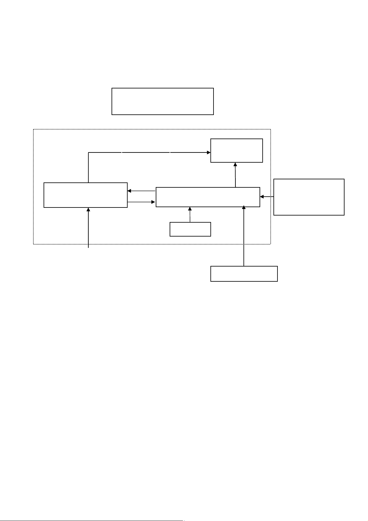
2. LCD Monitor Description
The LCD MONITOR will contain a main board, a power board, and a key board which house the flat panel control
logic, brightness control logic and DDC.
The power board will provide AC to DC Inverter voltage to drive the backlight of panel and the main board chips
each voltage.
Monitor Block Diagram
CCFL Driver
(Include: adapter, inverter)
Power board
AC-IN
100V-240V
Main Board
Key board
Flat Panel and
CCFL backlight
HOST Computer
RS232 Connector
For white balance
adjustment in factory
mode
Video signal DDC
5
Page 6
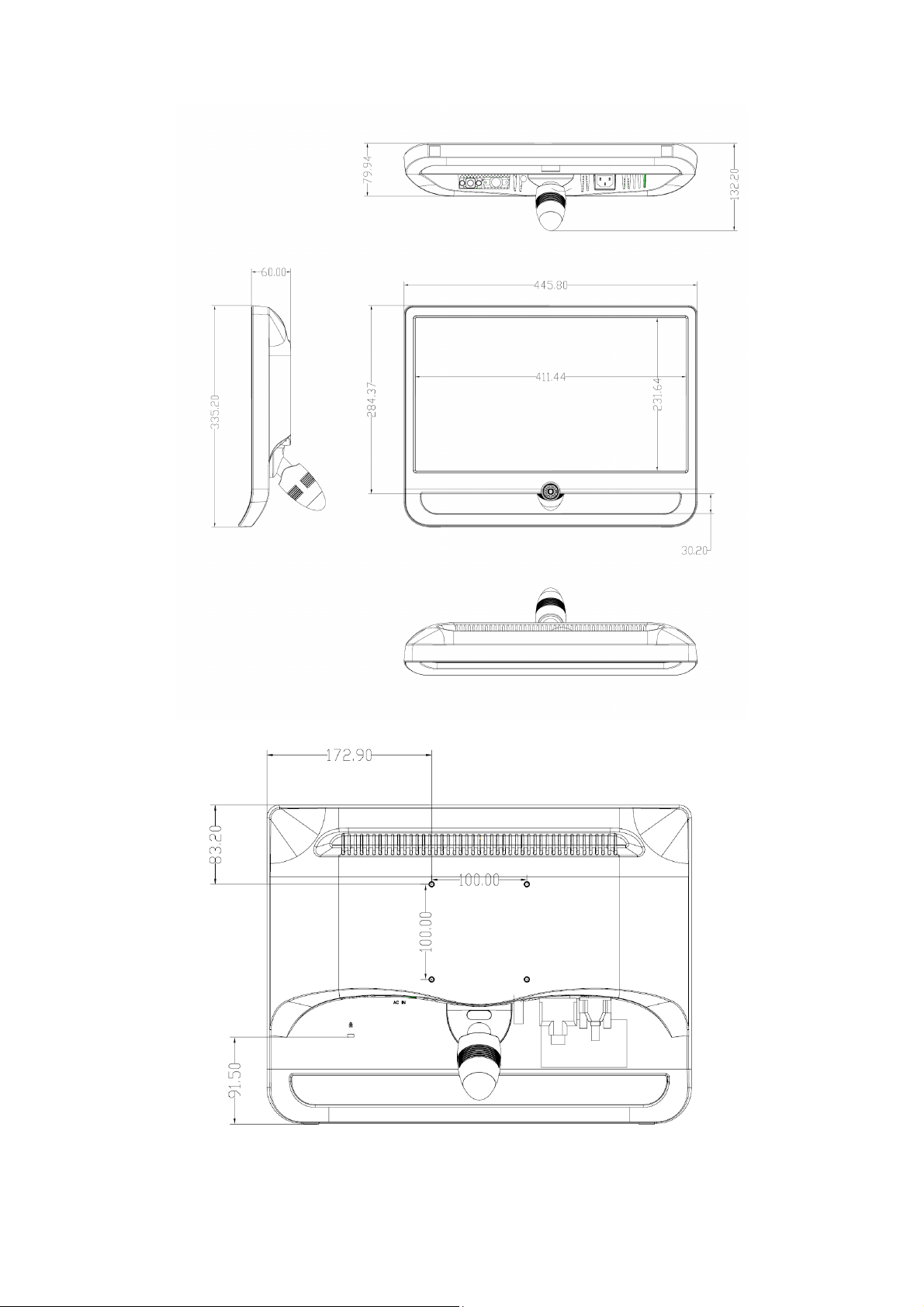
View and Dimension
6
Page 7
3. Operating Instructions
3.1 General Instructions
Press the power button to turn the monitor on or off. The other control buttons are located at front panel of the
monitor.
By changing these settings, the picture can be adjusted to your personal preferences.
- The power cord should be connected.
- Connect the video cable from the monitor to the video card.
- Press the power button to turn on the monitor, the power indicator will light up.
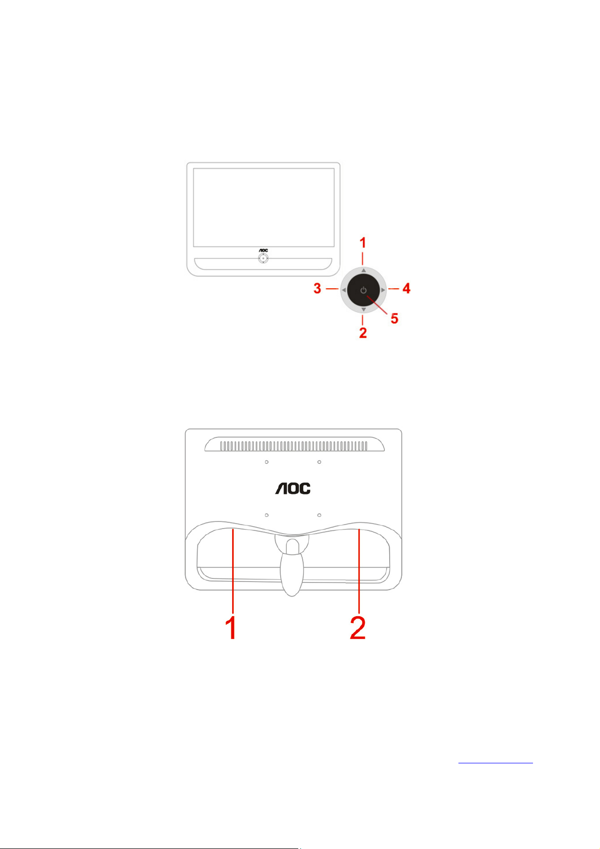
3.2 Control Buttons and Connections
1 Eco mode(DCR) / Up
2 Auto / Down
3 Contrast / Left
4 4:3 or wide / Right
5 Menu / Power
1. Power
2. Analog
Turn off your computer before performing the procedure below.
1. Connect the power cable to the AC port on the back of the monitor.
2. Connect one end of the 15-pin D-Sub cable to the back of the monitor and connect the other end to the
computer's D-Sub port.
3. Turn on your monitor and computer.
If your monitor displays an image, installation is complete. If it does not display an image, see Troubleshooting
7
.
Page 8
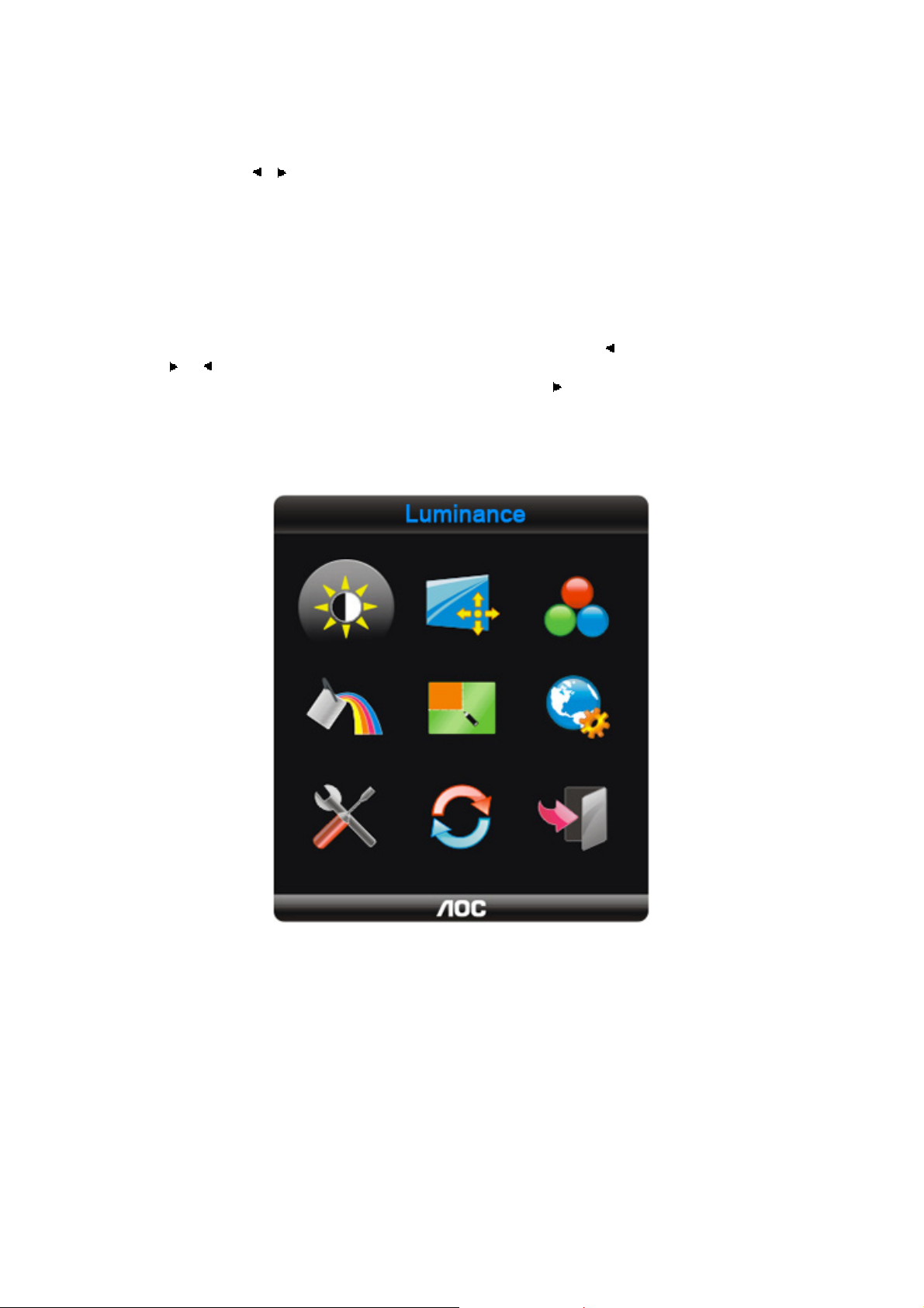
3.3 OSD Settings
• Press the Menu (Power) button to activate the OSD window. Press left, right, up, down button to navigate
through the functions. Once the desired function is highlighted, press the Menu (Power) button to activate
sub-menu .
• In sub-menu, Press up, down button to navigate through the functions. Once the desired function is
highlighted, press
superior menu.
• If you want to adjust any other function, repeat steps 1-2.
• To exit OSD windows, select “exit” icon on main OSD, then press the Menu (Power) button .
• OSD Lock Function: To lock the OSD, press and hold the Left button while the monitor is off and then press
power button to turn the monitor on. To un-lock the OSD - press and hold the Left button while the monitor is
off and then press power button to turn the monitor on.
• Eco Mode and DCR hot key : Press the Eco key continuously to select the Eco mode of brightness and DCR
on when there is no OSD ( Eco mode hot key may not be available in all models).
• Contrast adjustment hot key : When there is no OSD , press Contrast (
press or to adjust Contrast.
• 4:3 or wide image ratio hot key: When there is no OSD, press
ratio. (If the product screen size is 4:3 or input signal resolution is wide format, the hot key is disalbe to
adjust.)
• Auto configure hot key: When the OSD is closed, press Auto button will be auto configure hot key function .
• Press the Power button continuously about 2 second to turn off the monitor.
, button to button to change the setting. Press Menu (Power) button to return to
) to active Contrast adjustment bar,
continuously to change 4:3 or wide image
8
Page 9
Function Control Illustration
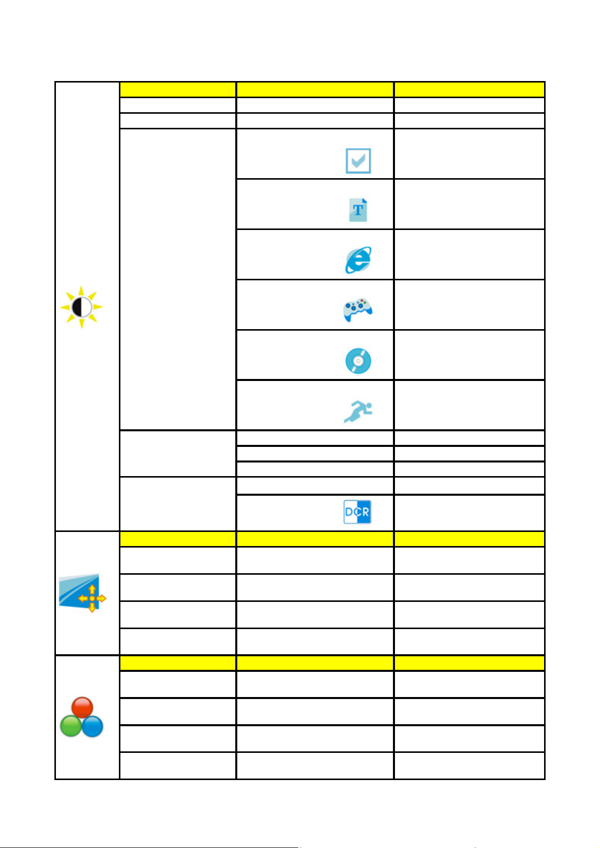
Luminance Adjust Range Description
Brightness 0-100 Backlight Adjustment
Contrast 0-100 Contrast from Digital-register.
Eco mode
Gamma1 Adjust to Gamma1
Gamma
Gamma2 Adjust to Gamma 2
Gamma3 Adjust to Gamma 3
DCR
Image Setup
Clock 0-100
Phase 0-100
H.Position 0-100
V.Position 0-100
Color Temp.
Warm
Normal
Cool
sRGB
6500K
7300K
9300K
Standard
Text
Internet
Game
Movie
Sports
Off
On
Standard Mode
Text Mode
Internet Mode
Game Mode
Movie Mode
Sports Mode
Disable dynamic contrast ratio
Enable dynamic contrast ratio
Adjust picture Clock to reduce
Vertical-Line noise.
Adjust Picture Phase to reduce
Horizontal-Line noise
Adjust the horizontal position of
the picture.
Adjust the verticalposition of the
picture.
Recall Warm Color Temperature
from EEPROM.
Recall Normal Color
Temperature from EEPROM.
Recall Cool Color Temperature
from EEPROM.
Recall SRGB Color Temperature
from EEPROM.
9
Page 10
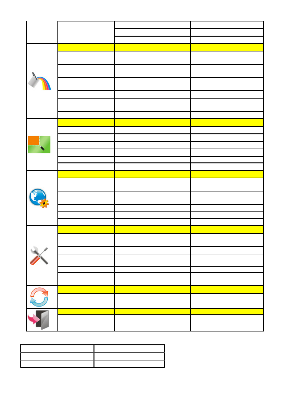
A
Red Red Gain from Digital-register
User
Green Green Gain Digital-register.
Blue Blue Gain from Digital-register
Color Boost
Full Enhance on or off
Nature Skin on or off
Green Field on or off
Sky-blue on or off Disable or Enable Sky-blue Mode
AutoDetect on or off
Disable or Enable Full Enhance
Mode
Disable or Enable Nature Skin
Mode
Disable or Enable Green Field
Mode
Disable or Enable AutoDetect
Mode
Demo on or off Disable or Enable Demo
Picture Boost
Frame Size 14-100 Adjust Frame Size
Brightness 0-100 Adjust Frame Brightness
Contrast 0-100 Adjust Frame Contrast
H. position 0-100 Adjust Frame horizontal Position
V.position 0-100 Adjust Frame vertical Position
Bright Frame on or off Disable or Enable Bright Frame
OSD Setup
H.Position 0-100
V.Position 0-100
Timeout 5-120 Adjust the OSD Timeout
Adjust the horizontal position of
OSD
Adjust the vertical position of
OSD
Transparence 0-100 Adjust the transparence of OSD
Language Select the OSD language
Extra
Input Select Analog
Auto Config yes or no
Image Ratio wide or 4:3
Select Analog Sigal Source as
Input
uto adjust the picture to default
Select wide or 4:3 format for
display
DDC-CI yes or no Turn ON/OFF DDC-CI Support
Information
Show the information of the main
image and sub-image source
Reset
Reset yes or no Reset the menu to default
Exit
Exit Exit the main OSD
LED Indicators
Status LED Color
Full Power Mode Green or Blue
Active-off Mode Orange or red
10
Page 11
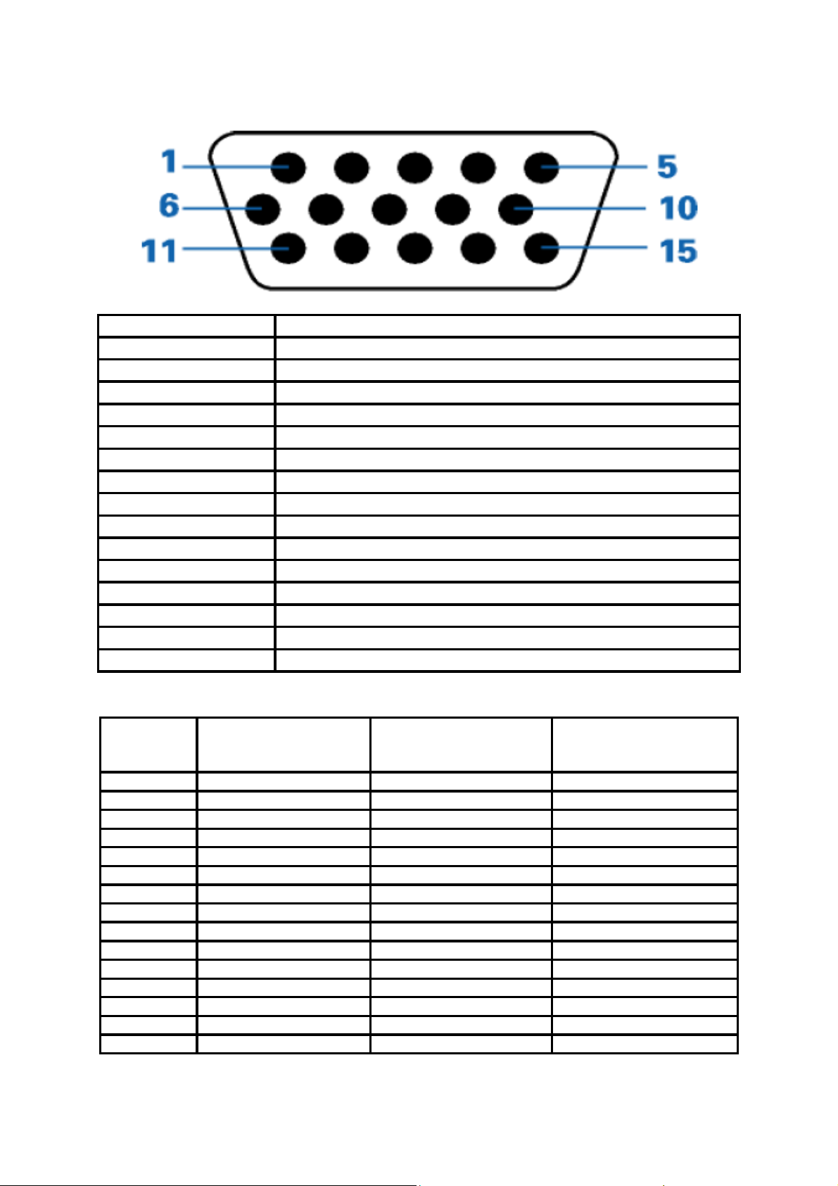
4. Input/Output Specification
4.1 Input Signal Connector
Pin Number 15-Pin Side of the Signal Cable
1 Video-Red
2 Video-Green
3 Video-Blue
4 N.C.
5 Detect Cable
6 GND-R
7 GND-G
8 GND-B
9 +5V
10 Ground
11 N.C.
12 DDC-Serial data
13 H-sync
14 V-sync
15 DDC-Serial clock
4.2 Factory Preset Display Modes
HORIZONTAL
STAND RESOLUTION
FREQUENCY(kHZ)
VGA 640 x 480 @60Hz 31.469 59.940
VGA 640 x 480 @72Hz 37.861 72.809
VGA 640 x 480 @75Hz 37.500 75.000
Dos-mode 720 x 400 @70Hz 31.469 70.087
SVGA 800 x 600 @56Hz 35.156 56.250
SVGA 800 x 600 @60Hz 37.879 60.317
SVGA 800 x 600 @72Hz 48.077 72.188
SVGA 800 x 600 @75Hz 46.875 75.000
Mac-mode 832 x 624 @75Hz 49.725 74.500
XGA 1024 x 768 @60Hz 48.363 60.004
XGA 1024 x 768 @70Hz 56.476 70.069
XGA 1024 x 768 @72Hz 57.500 72.074
XGA 1024 x 768 @75Hz 60.023 75.029
XGA 1024 x 768 @75Hz 47.712 74.927
WSXGA 1366 x 768 @60Hz 47.765 59.85
VERTICAL
FREQUENCY(Hz)
11
Page 12
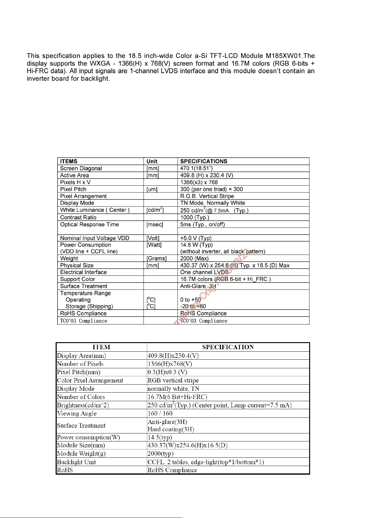
4.3 Panel Specification
4.3.1 General Features
AUO M185XW01
CPT CLAA185WA03
CLAA185WA03_V2 is 18.51” color TFT-LCD (Thin Film Transistor Liquid Crystal Display) module composed of LCD
panel, driver ICs, control circuit and backlight. By applying 6bit+Hi-FRC digital data,1366*768, 16.7M-color images
are displayed on the 18.51” diagonal screen. Input power voltage is 5.0V for LCD driving. Inverter for backlight is not
included in this module. General specification are summarized in the following table:
4.3.2 GENERAL SPECIFICATIONS
AUO M185XW01
(Ta= 25±2℃)
CPT CLAA185WA03
12
Page 13
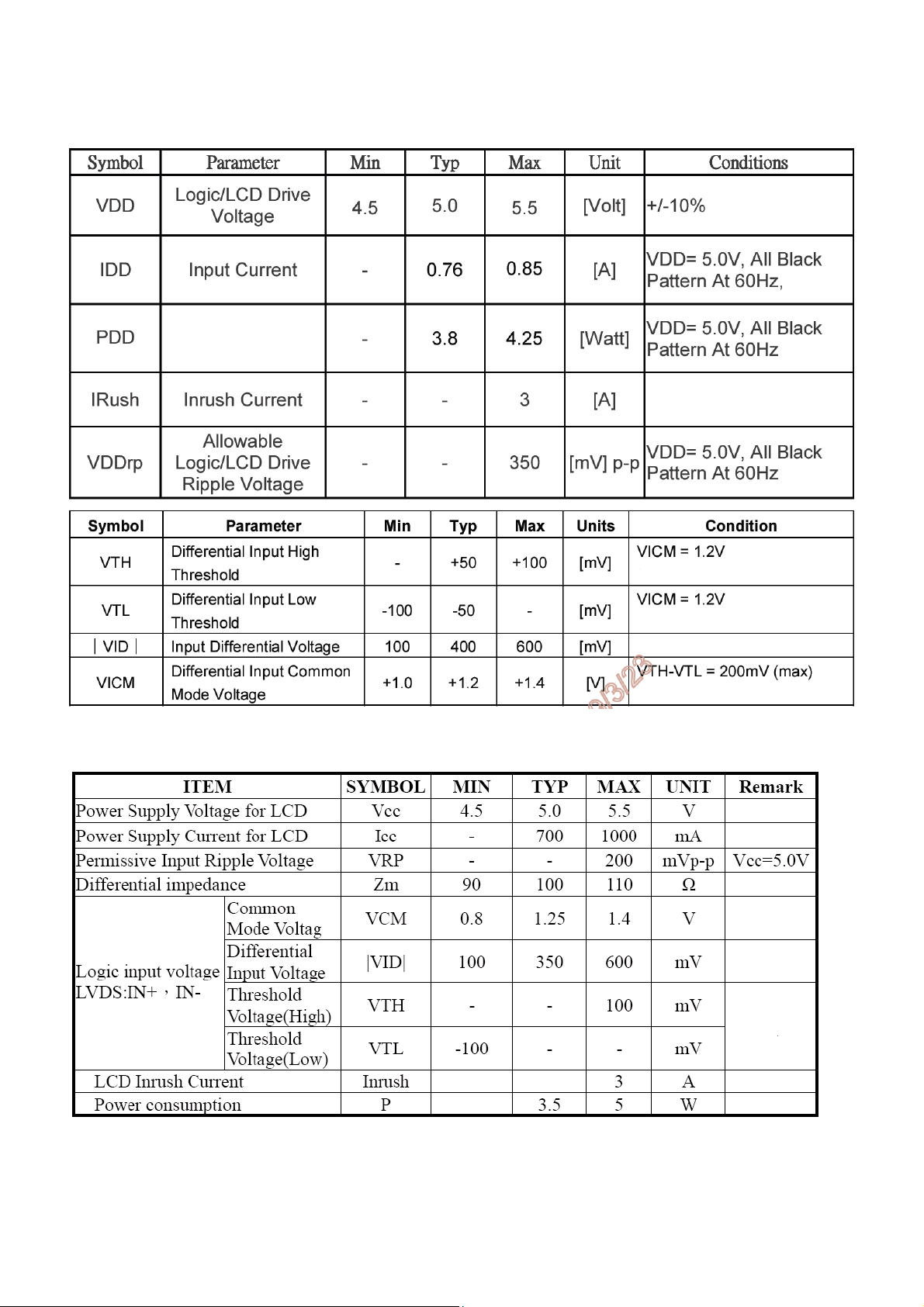
4.3.3 Electrical Characteristics
1. TFT LCD Module
AUO M185XW01
(Ta= 25±2℃)
CPT CLAA185WA03
Ta= 25±2℃,VCC=5.0V, Fh=47.28KHz, Fv=60Hz, Fclk=67.1MHz.
13
Page 14
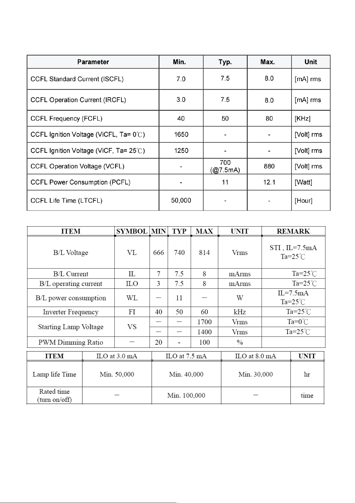
2 .BackLight Unit
AUO M185XW01
(Ta= 25±2℃)
CPT CLAA185WA03
14
Page 15
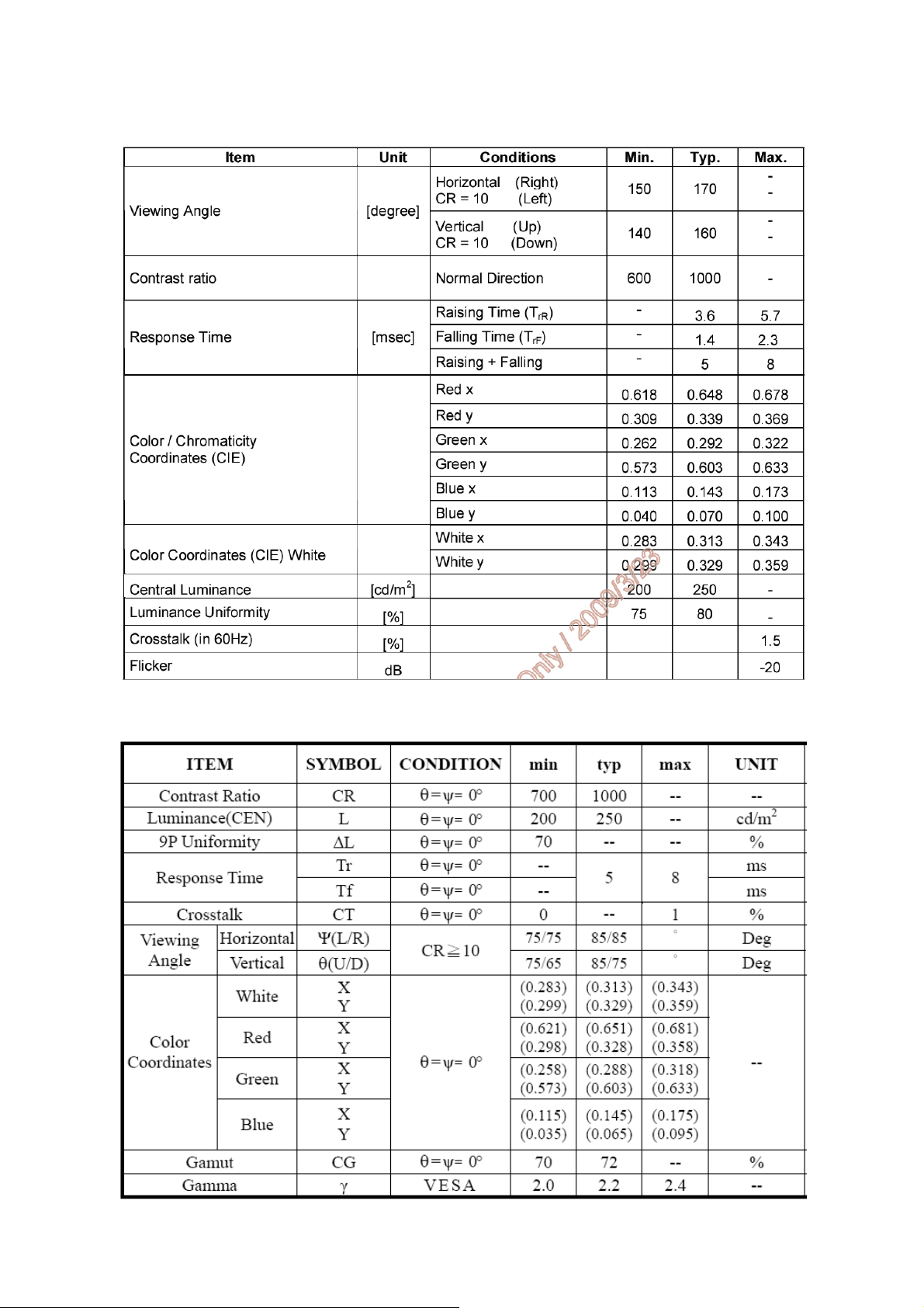
4.3.4 Optical Characteristics
AUO M185XW01
(Ta= 25±2℃)
CPT CLAA185WA03
Ta=25℃,VCC=5.0V
15
Page 16
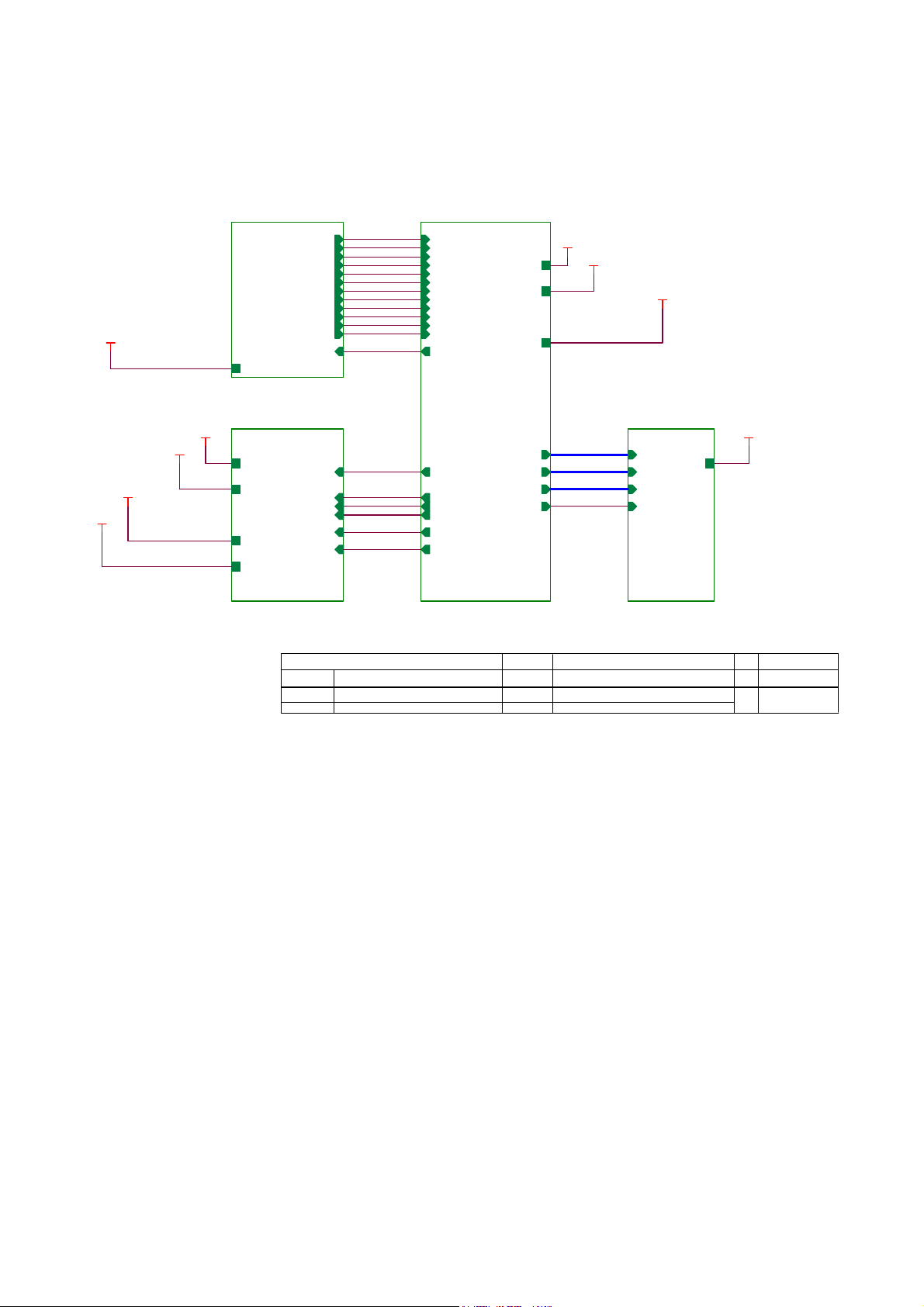
5. Block Diagram
5.1 Main Board
715G3244 2 2
TSUM1PFR SCHEMATIC
CMVCC1
CMVCC1
CMVCC
XGA/SXGA
02.Input
VCC1.8
VCC3.3
05.Power
CMVCC1
VCC1.8
VCC3.3
CMVCC
CMVCC1
DSUB_R+
DSUB_RDSUB_G+
DSUB_G-
DSUB_SOG
DSUB_B+
DSUB_B-
DSUB_H
DSUB_V
DDC1_SDA
DDC1_SCL
DET_CABLE
EDID _CTRL
on_BACKLI GHT
Mut e
Volume#
PANEL_I D#
Adj_BACKLI GHT
VCTRL
DSUB_R+
DSUB_RDSUB_G+
DSUB_GDSUB_SOG
DSUB_B+
DSUB_BDSUB_H
DSUB_V
DDC1_SDA
DDC1_SCL
DET_CABLE
EDID _CTRL
on_BACKLI GHT
Mut e
Volume#
PANEL_ID#
Adj_BACKLIGHT
VCTRL
03.Scalar
LVDS OUTPUT
VCC1.8
VCC1.8
VCC3.3
CMVCC1
PA[0. .1]
PA[4. .9]
PB[0. .9]
PPWR_O N#
VCC3. 3
PA[0.. 1]
PA[4.. 9]
PB[0.. 9]
CMVCC1
PA[0..1]
PA[4..9]
PB[0..9]
PPWR_ ON#
04.Output
CMVCC
CMVCC
T P V ( Top Victory Electronics Co . , Ltd. )
絬 隔 瓜 絪 腹
Key Component
G3244-2-2-X-8-100426
01.Top
Date
OEM MO DE L Size
TPV MO D EL
PCB NAME
A1981Wx A
T99SRD* TVN N F
G3244-2-2
Sheet
of
37Thursday , May 06, 2010
Rev
称爹
称爹
>
<
16
Page 17
t
t
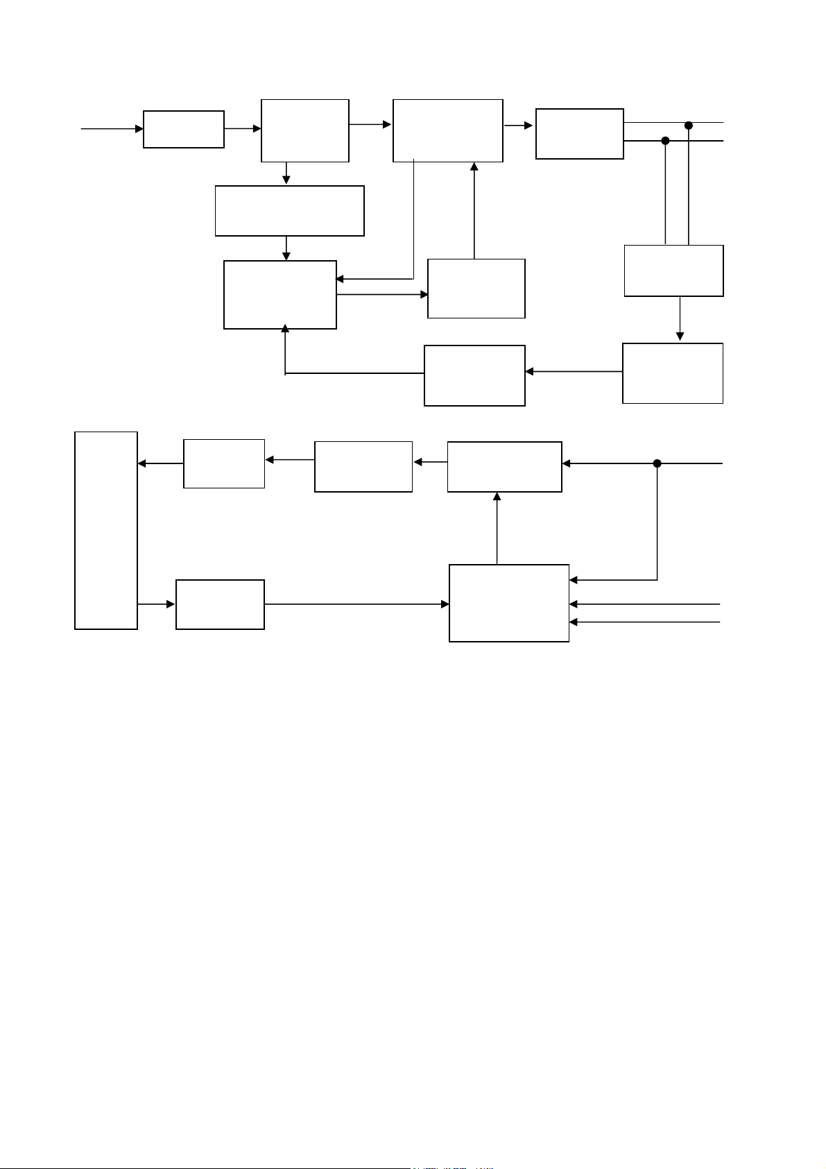
5.2 Power Board
715G2852 2 11
AC input
EMI filter
B/L
PWM Control
Output
Circui
Feedback
Circui
Bridge
Rectifier
and Filter
Start Resistor
(R904,R932)
LD7575A
(IC901)
Transformer
(T801)
Transformer
(T901)
Power Switch
(Q901)
Photo coupler
(IC902)
MOSFET
PWM Control
TL494IDR
(Q802)
(IC801)
Rectifier
diodes
12V
5V
Feedback
Circuit
Regulator
(IC903)
12V
ON/OFF
DIM
17
Page 18
6. Schematic
6.1 Main Board
715G3244 2 2
GND POWER
DSUB_SCL
DSUB_SDA
DGND
H_Sync
V_Sy nc
15
14
13
12
11
R101 0R05 1/10W 5%
R105
2K2 1/16W 5%
CN101
DB15
10
VGA_PLUG
5
9
DSUB_5V
4
8
3
7
2
6
1
17 16
VGA_G+
VGA_R+
1
2
3 4
1
2
3 4
DSUB_SDA
DSUB_SCL
R106
2K2 1/16W 5%
VGA_BVGA_B+
VGA_GVGA_G+
VGA_RVGA_R+
U103
AZC199-04S
I/O1
I/O4
GND
VDD
I/O2 I/O3
U102
AZC199-04S
I/O1
I/O4
GND
VDD
I/O2 I/O3
ZD103
RLZ5.6B
6
5
6
5
H_Sync
ESD_5V
V_Sy nc
候綼
VGA_PLUG
ESD_5V
VGA_B+
候綼
C102
22pF
U103
U102
R102 100R 1/16W 5%
R103 100R 1/16W 5%
C103
22pF
DSUB_5V
C114
NC
C115
NC
DDC1_SDA5
DDC1_SCL5
DSUB_SCL
DSUB_SDA
DDC1_SDA
DDC1_SCL
DSUB_H 5
DSUB_V 5
R475 47R 1/16W 5%
R476 47R 1/16W 5%
VGA_B+
VGA_B-
VGA_G+
VGA_G-
VGA_R+
VGA_R-
R472
4K7 1/16W 5%
CMVCC1
ESD_5V
R473
4K7 1/16W 5%
FB102
1 2
BEAD
FB103
1 2
BEAD
FB101
1 2
BEAD
DSUB_5V
2
3
R474
4K7 1/16W 5%
1
D403
BAV70
8
7
6
VCC
WP
SCL
R107
75R 1/16W 5%
R112
75R 1/16W 5%
R116
75R 1/16W 5%
U405
1
A0
2
A1
3
A2
45
GNDSDA
AT24C02BN- SH-T
R104
100R 1/16W 5%
C104
5pF/50V
R108
100R 1/16W 5%
R109
390 OHM 1/16W
R111
100R 1/16W 5%
C108
5pF/50V
R114
100R 1/16W 5%
R115
100R 1/16W 5%
C111
5pF/50V
R117
100R 1/16W 5%
C434
0.22uF16V
Q407
LMBT3904LT1G
VGA_PLUG
C101
0.047uF
C105
0.047uF
C106
C107
0.047uF
C109
0.047uF
C110
0.047uF
C113
0.047uF
CMVCC1
1000pF
R118
10K 1/16W 5%
R122
NC
DSUB_B+ 5
DSUB_B- 5
DSUB_SOG 5
DSUB_G+ 5
DSUB_G- 5
DSUB_R+ 5
DSUB_R- 5
CMVCC1 5,6,7
DET_CABLE 5
EDID_CTRL 5
T P V ( Top Victory Electronics Co . , Ltd. )
Date
G3244-2-2-X-8-100426
02.Input
絬 隔 瓜 絪 腹
Key Component
OEM MOD EL Size
A1981Wx
TPV MO DEL
T99SRD*TVNN F
G3244-2-2
PCB NAME
Sheet
47Thursday, May 06, 2010
of
Rev
称爹
B
<
称爹
>
18
Page 19

CN408
CONN
CN409
NC/CONN
SST
For user data, WB, EDID,
HDCP are saved in
Eon
Flash.
SST
Befor AOC ID2007 OSD
010A
020A
For ID2008 ID2009
Eon
For All model
020
VCC3.3
C408
0.22uF16V
R408
10K 1/16W 5%
CMVCC1
CMVCC14,6,7
NC/10uF /50V
6
5
4
3
2
1
7
6
5
4
3
2
1
10K 1/16W 5%
ZD404
NC/MLVS0603M04
C410
1 2
U402
U402
U402
+
R421
VCC3.3
R487
4.7K1/16W
1
CS#
2
DO
WP
3
WP#
4 5
VSS DI
R417
NC/10K 1/ 16W 5%
3.9K OHM 1/16W
12
C413
MLVS0402M04
CS
U402
VCC
HOLD#
CLK
MX25L2026MI-12G
VCC3.3
R427
ZD402
C414
12
1 2
NC/M LVS0603M04
Near to Connect
8
7
6
MLVS0402M04
DSUB_R+4
DSUB_R-4
DSUB_G+4
DSUB_G-4
DSUB_SOG4
DSUB_B+4
DSUB_B-4
DSUB_H4
DSUB_V4
DDC1_SDA4
DDC1_SCL4
AVDD
CS
R405 100R 1/16W 5%
C411
22pF
X401
14.31818MHz
C412
22pF
1 2
R428
3.9K OHM 1/16W
LED_GRN/BLUE
LED_ORANGE/TOU CH VCC
LED_ORANGE/TOU CH VCC
LED_ORANGE/TOU CH VCC
ZD403
C415
12
1 2
NC/M LVS0603M04
MLVS0402M04
LED_ORANGE/TOUCH VCC
R403 390 OHM 1/16W
C401
0.1uF/16V
R401
100R 1/16W 5%
0R05 1/16W
R402
KEY1
KEY2
POWER_KEY#
C416
0.1uF/16V
U401
13
RIN0P
12
RIN0M
10
GIN0P
9
GIN0M
11
SOGIN0
8
BIN0P
7
BIN0M
16
HSYNC0
17
VSYNC0
18
DDCA_SD A/RS232_TX
19
DDCA_SC L/rs232_RX
4
REXT
15
REFP
14
REFM
21
SDO
22
SCZ
23
SCK
24
SDI
28
GPIO_P27/PWM1
54
RST
1
XIN
2
XOU T
31
MODE [0]
32
MODE [1]
R404
10K 1/16W 5%
VCC3.3
R461 0R05 1/16W
R462 0R05 1/16W
R478 NC
C417
0.1uF/16V
FB404
NC
FB405
NC
NC/R LZ5.6B
R463 NC
R464 NC
ZD401
VCC3.3
AVDD
6
AVDD_ADC
GND
GND
5
29573
R407
10K 1/16W 5%
TOUCH POWER
VCC1.8
51
VDDP
LVDS
GPIO_P11/I2C_MDA
GND
RTD2270S-GR
C433
NC
30
53
VCTRL
VDDC
VDDC
LVA3P
LVA3M
LVA2P
LVA2M
LVA1P
LVA1M
LVA0P
LVA0M
LVB3P
LVB3M
LVBCKP
LVBCKM
LVB2P
LVB2M
LVB1P
LVB1M
LVB0P
LVB0M
GPIO_P15/PWM0
PWM2/GPIO_P24
GPIO_P12
PWM1/GPIO_P25
RSTN
GPIO_P00/SAR1
GPIO_P01/SAR2
GPIO_P06
GPIO_P07
PWM0/GPIO_P26
GPIO_P13
GPIO_P14
GPIO_P10/I2C _MCL
CN406
1
2
3
4
5
6
7
8
NC/CONN
CN402
1
2
3
4
5
6
NC/CONN
CN407
1
2
3
4
5
6
7
NC/CONN
52
PA0
33
34
PA1
PA4
35
36
PA5
37
PA6
38
PA7
39
PA8
PA9
40
PB0
41
42
PB1
43
PB2
PB3
44
45
PB4
46
PB5
PB6
47
PB7
48
49
PB8
50
PB9
20
R424 NC
27
55
56
R411 100R 1/16W 5% KEY2
58
R412 100R 1/16W 5%
59
60
R414 10K 1/16W 5%
61
R410 10K 1/16W 5%
62
R418 NC/100OHM1/16W
63
64
R419 NC/100OHM1/16W
Max condition for LED:
1. Vcc = 3.3 V
2. Current = 12 mA
FW need to be modified.
26
25
R413 100R 1/16W 5%
R466
2K2 1/16W 5%
LED_G/B
R469
2K2 1/16W 5%
LED_O
When use touch
Key,GPIO_P07 as
to control touch
key VCC
PA[0..1]
PA[4..9]
PB[0..9]
KEY1
CMVCC1
Q403
LMBT3906LT1G
PA[0..1] 6
PA[4..9] 6
PB[0..9] 6
R425
NC
LED_G/B
LED_O
R468 200R 1/10W 5%
R481
0R05 1/16W
R482 NC
Q402
LMBT3906LT1G
R471 330R 1/10W 5%
VCTRL 7
EE_WP
C418
NC
on_BACKLIGHT 7
adj_BACKLIGHT 7
Volume# 7
Mute 7
PPWR_ON# 6
DET_CABLE 4
LED_GRN/BLUE
CMVCC1
VCC3.3
LED_ORANGE/ TOUCH VCC
R485 4K7 1/16W 5%
R426 NC
R452 NC
R420 100R 1/16W 5%
R451 NC
MSCL
MSDA
For NVRAM
M24C04-WMN6TP
U403
0.22uF16V
C419
R424
100R 1/16W 5%
100R 1/16W 5%
R451
100R 1/16W 5%
R452
R453
10K 1/16W 5%
10K 1/16W 5%
R454
R455
10K 1/16W 5%
R426
R420
絬 隔 瓜 絪 腹
Key Component
VCC3.3
VCC3.37
VCC1.87
EDID_CTRL 4
PANEL_ID# 7
MSDA
POWER_KEY#
MSCL
R453
NC
FB401
30OHM
C403
0.1uF/16V
VCC1.8
C406
0.1uF/16V
R454
R455
NC
NC
EE_WP
Without NVRAM
NC
NC
T P V ( Top Victory Electronics Co . , Ltd. )
Date
NC or 100R 1/16W 5%
NC or 100R 1/16W 5%
G3244-2-2-X-8-100426
03.Scalar
AVDD
C404
1UF 10V
C407
0.1uF/16V
VCC3.3
C429
NC
1
NC
2
E1
3
E2
45
VSSSDA
When NVRAM is used,
POWER_KEY# and PANEL_ID#
will not be used at same
time.
R425, C418 depend on
case.
PANEL_ID# and POWER_KEY#
could be optional.
NC
NC
NC
NC
NC
NC
U403
8
VCC
7
WC
6
SCL
NC/M24C04-WMN6TP
NC
NC
OEM MOD EL Size
A1981Wx
TPV MOD EL
T99SRD*TVNN F
G3244-2-2
PCB NAME
of
57Thursday, May 06, 2010
Sheet
C
Rev
<
称爹
>
称爹
19
Page 20

PA[0..1]5
PA[4..9]5
PB[0.. 9]5
PA[0..1]
PA[4..9]
PB[0. .9]
PA0
PA1
PA4
PA5
PA6
PA7
PA8
PA9
PB0
PB1
PB2
PB3
PB4
PB5
PB6
PB7
PB8
PB9
NC/R477
150R 1/4W 5%
PANEL_VCC
R434
330OHM1/4W
3
1
G
AO3401L
CN403
1
2
C420
0.1uF/16V
PA0
PA1
PB2
PB3
PA4
PA5
PA6
PA7
PA8
D
2
S
PA9
PB0
PB1
PB2
PB3
PB4
PB5
PB6
PB7
PB8
PB9
3
4
5
6
7
8
9
10
11
12
13
14
15
16
17
18
19
20
21
22
23
24
25
26
27
28
29
30
PA1
PB3
PA5
PA7
PA9
PB3
PB5
PB7
PB9
PANEL_VCC
CN405
1
3
5
7
9
11
13
15
17
19
21
23
25
27
29
NC/CONN
2
4
6
PA0
8
PB2
10
12
PA4
14
PA6
16
PA8
PB0PB1
18
20
PB2
PB4
22
24
PB6
26
PB8
28
30
2006-11-7 Add pull up 4K7 to MVCC
R435
4K7 1/16W 5%
PPWR _ON#5
PPWR _ON#
R433
10K 1/16W 5%
R436
100K 1/16W 5%
Q404
LMBT3906LT1G
絬 隔 瓜 絪 腹
Key Component
CMVCC
C419
0.1uF/16V
123
4
Q411
SSS
Q405
AO3401
T P V ( Top Vic tory Electronic s Co . , Ltd. )
G3244-2-2-X-8-100426
04.Output
Date
G
D
5
DDD
876
120OHM
NC/ AO4411
FB402
20
CONN
CMVCC 4,5,7
PANEL_VCC
C421
+
100uF/25V
OEM MOD EL Size
TPV MOD E L
PCB NAME
Sheet
A1981Wx
T99SRD*TVNN F
G3244-2-2
67Thursday , May 06, 2010
of
Rev
称爹
<
A
称爹
>
Page 21

CN404
CONN
9
8
7
6
5
4
3
2
1
CMVCC4,5,6
CMVCC
CMVCC
BKLT-VBRI
BKLT-EN
C_PANEL_INDEX
Volume
Mute
CMVCC
R450 NC
NC(R 0402)
PANEL_ID# 5
CMVCC1
R449
NC
CMVCC1 4,5,6
Mute 5
BKLT-EN
C425
NC
CMVCC1
R465
NC
VCC3.3
R437
10K 1/16W 5%
Q406
2N3904S-RTK/PS
VCC3.3
R440
4K7 1/16W 5%
R439
10K 1/16W 5%
on_BACKLIGH T 5
VCC3.3
R480
2.2 OHM 2W
R479
NC
VCTRL5
2 3
1
Q410
MMBT2907AK
2 3
1
Q409
MMBT2907AK
C432
0.1uF/ 16V
VCC1. 8
+
C423
100uF/25V
VCC1. 8 5
BKLT-VBRI
VCC3.3
R441
1K 1/16W 5%
R442
100R 1/16W 5%
adj_BACKLIGH T 5
Volume
VCC3. 3
R446
NC/ 10K 1/16W 5%
Q408
NC/ 2N3904S-RTK/PS
R486
NC
R448
NC/ 4.7K1/16W
VCC3. 3
R447
NC/ 10K1/16W
Volume# 5
CMVCC1
+
MVC C
C426
NC/ 100uF/25V
C428
0.1uF/ 16V
FB403 NC
VIN
VOUT
ADJ(GN D)
U404
3
2
1
C422
0.1uF/ 16V
U404 can use package 223 or 252.
T P V ( Top Victory Electronics Co . , Lt d. )
Date
G3244-2-2-X-8-100426
05.Power
絬 隔 瓜 絪 腹
Key Component
VCC3.3
VCC3.3 5
C427
+
100uF/25V
OEM MODEL Si ze
A1981Wx
TPV MODEL
T99SRD*TVNN F
G3244-2-2
PCB NAME
Sheet
77Thursday , May 06, 2010
of
Rev
称爹
B
<
称爹
>
21
Page 22

6.2 Power Board
715G2852 2 11
1
!
+
2
BD901
-
KBP208G
4
C904
0.22UF
!
R900
680K OHM 1/4W
!
t
C902
1000pF
!
NR901
NTCR
2
3
1
4
!
C908
0.22UF
R902
680K OHM 1/4W
!
VAR901
Varistor
N.C
3
CN901
SOCKET
87G 501 32 S
C901
1000pF
L901
30mH
12
!
3
!
!
!
!
R901
680K OHM 1/4W
!
!
100K OHM 1% 1/8W
!
F901
FUSE
C907
+
82uF 450V
C938
NC
C911
0.1uF
IC901
1
RT
2
COMP
3
CS
4 5
GNDOUT
R915
C928
0.01uF
HEAT SINK(Q901_Q90G6263-6)
LD7575A PS
GND1
GND
1
2
HS2
HEAT SINK(D906_Q90G6263-6)
1
2
HS3
1
2
R904
10K OHM 1/4W
R932
10K OHM 1/4W
HV
NC
VCC
R918
100 OHM 1/4W
R919
100 OHM 1/4W
R920
100 OHM 1/4W
!
T901
!
9
10
7
8
11
12
POWER X'FMR
12
43
R961 100 OHM 1/4W
R962 100 OHM 1/4W
R935 100 OHM 1/4W
IC902
PC123X2YFZOF
C924
0.1uF
IC903
AZ431AZ -AE1
R921
R922
R923NC
4
5
6
2
1
C900
3300pF 250V
R905
NC
R906
NC
D901
FR103
C903
+
22uF/50V
R907
NC
D903
LL4148
8
7
6
R910
10R 1/4W
ZD905
RLZ18B
R912
220 OHM 1/4W
C909
470pF/25 V
HS5
SHIELD(H85G0002-1)
1
2
1 2
C906
1500pF2KV
R938
10K 1/8W
R908
100KOHM +-5% 2WS
D900
FR107
R909
5.1 OHM 1/4W
!
Q901
2SK2645-54MR
R914
0.47 OHM +-5% 2WS
C912
0.001uF
2
1
3
D906
FCH10U 10
D907 NC
NC
NC
D905 31DQ06FC3
C929
0.001uF
R925
1K 1/8W
R926
1K 1/10W 1%
C925
NC
T P V ( Top Victory Electronics Co . , Ltd. )
絬 隔 瓜 絪 腹
Key Component
Date
C917
680uF/25V
C910
NC
+
2.POWER
L904
1.0uH
+
+
C918
680uF/25V
L905
NC
C921
NC
C939
+
NC
C940
1000uF16V
R924
150R 1/8W
2.43K OHM 1% 1/10W
G2852-3-4-X-6-090818
+
NC
L903
1.0uH
RLZ5.1B
LL4148
1K 1/10W 1%
C922
+
470PF50V
ZD923
NC
R948
NC
Q904
ZD922
D916
R942
R930
1 2
R947
NC
R952
NC
ZD921
1 2
OEM MODEL Size
TPV MOD EL
PCB NAME
Sheet
RLZ13B
1 2
R940
R927
3.6K OHM 1% 1/10W
PWPC9821G HD1 A
715G2852-3-4
24Tuesday, Augus t 18, 2009
33K 1/10W
D915
LL4148
VOL
MUTE
+5V
DIM
ON/OF F
F19S
of
R946
150 OHM 2W
Q903
PMBS3904
C932
C915
470uF/16V
C931
0.1uF
0.001uF
+
1 2
R943
470R 1/8W
R939
1K 1/8W
NC
Rev
称爹
ZD902
RLZ13B
F902
NC
F904
F903
NC
F905
0 OHM 1/4W
C930
0.1uF
CN902
1
2
3
4
5
6
7
8
9
10
CONN
Custom
OD M MODEL
+12V
+5V1
+5V
22
Page 23

1
2
D801
BAV99
D802
BAV99
CONN
CN801
2
1
1
2
CONN
CN802
2
1
ON/OFF
C839
1500PF/50V
R855
+12V
DIM
F801
0 OHM 1/4W
Q805
PDTC144WK
C807
0.1uF/25V
R804
100R 1/8W
Q808
PDTA144WK
C825
0.1uF/25V
PMBS3904
PMBS3906
Q801
Q804
23
1
Q811
PMBS3904
D810
NC
R839
22R 1/8W
D811
NC
470PF50V
C802
C824
+
0.1uF
Q802
AM9945N-T1-PF
1
S
2
G
3
S
4
G
15R 1/4W
R856
15R 1/4W
8
D
7
C838
D
1500PF/50V
6
D
5
D
6
3
4
T801
POWER X'FMR
R821
1K 1/8W
3
R801
1K5 1/10W 1%
R822
1K 1/8W
3
R814
1K5 1/10W 1%
7
C801
30pF/3KV
81
C803
30pF/3KV
D807
LL4148
D805
LL4148
C819
0.0022uF
C823
0.0022uF
R817
10K 1/10W 1%
R828
10K 1/10W 1%
1
R861
NC
Q807
N.C
23
R853
68K 1/10W
R850
22R 1/8W
1
2
3
4
5
6
7
8 9
R864
NC
穝糤
C817
NC
R841
68K OHM 1% 1/10W
R829
22R 1/8W
R825
22R 1/8W
TL494IDR
IC801
1IN+
1INFEEDBACK
DTC
OUTPUT CTRL
CT
RT
GND
C1 E1
R854
NC
R837
47K 1/8W
R807
R824
1K 1/10W 1%
10K 1/10W 1%
R808
10K 1/10W 1%
C845
2.2uF/16V
R862
1M 1/10W 5%
R803
680K 1/10W
D814
LL4148
R818
1K 1/10W 1%
Q809
RK7002
C846
NC
T P V ( Top Victory Electronics Co . , Lt d. )
絬 隔 瓜 絪 腹
Key Component
Date
C834
0.1uF/25V
G2852-3-4-X-6-090818
3.INVER TER
D806
LL4148
R835
1M 1/10W 5%
OEM MODEL Size
F19S
TPV MODEL
PWPC9821GHD 1 A
715G2852-3-4
PCB NAME
Sheet
34Tuesday, August 18, 2009
of
Custom
Rev
ODM MOD EL
称爹
16
2IN+
15
2IN-
14
REF
13
12
VCC
11
C2
10
E2
R826
1K 1/8W
D817
LL4148
6K8 1/10W
10K 1/10W 1%
R827
1K 1/10W 1%
R851
R830
NC
R820
R802
8.2K 1/10W 1%
C822
1uF/25V
D812
LL4148
10K 1/10W 1%
Q806
PMBS3904
C842
0.01uF
R863
C835
NC
R832
10K 1/10W 1%
R831
1K 1/8W
R823
0R05 1/10W 5%
C821
0.1uF/25V
51K OHM 1% 1/8W
R810
C820
220pF50V
R865
NC
新增
Q812
PMBS3906
23
Page 24

7. PCB Layout
7.1 Main Board
715G3244 2 2
24
Page 25

25
Page 26

7.2 Power Board
715G2852 2 11
26
Page 27

27
Page 28

7.3 Key Board
715G3010 1
28
Page 29

8. Maintainability
8.1 Equipments and Tools Requirement
1. Voltmeter.
2. Oscilloscope.
3. Pattern Generator.
4. DDC Tool with an IBM Compatible Computer.
5. Alignment Tool.
6. LCD Color Analyzer.
7. Service Manual.
8. User Manual.
29
Page 30

8.2 Trouble Shooting
1. No Power
No power
Check power cable is
tightened?
OK
Check Power “On/Off”
is “On”?
OK
Check the LED
indicate is OK?
NG
Re-plug the power cable
NG
Turn on the Power “On/Off” switch
NG
Check the AC power
OK
Replace the converter board
NG
Replace main board and check connections
NG
Replace key board and check connections
30
Page 31

2. No Video (Power LED Blue)
No Video (Power LED Blue)
Press the power
button is OK?
OK
Replace the converter
board
NG
Replace the main
board and connection
NG
Replace the main board
OK
The end
OK
The end
NG
Check the LVDS/FFC
cable or panel
NG
Replace the key board
OK
Replace the LVDS/FFC
cable or panel
31
Page 32

3. DIM
DIM (image overlap, focus or flicker)
Reset in factory mode
NG
OK
The end
Set to the optimal
frequency, select the
recommended frequency
NG
Readjust the phase and pixel
clock in the user mode
NG
Pull out signal cable and
check “Self Test Feature
Check” is ok?
OK
The end
OK
The end
OK
Check the signal cable
and the PC
NG
Replace the main board
NG
Replace the panel
OK
NG
OK
The end
32
Page 33

4. Color is not optimal
Miss color
Replace the signal cable
NG
Pull out the signal cable
and check the screen
color display is normal?
NG
Replace the main board
Replace the signal cable or PC
Color is not optimal
OK
The end
OK
Color shift
Reset the factory mode
NG
In the user mode, set the” color
settings” until customer satisfy
NG
33
Page 34

9. FOS Testing
9.1 Brightness Measurement
Max. Brightness >250 cd/㎡(typ).
Test conditions:
- Center of display
- Video input (RGB) = 0,700V for Analog Input
- Brightness control is set to max
- Contrast control is set to max.
Min. brightness measurement:
< 45% of Max luminance (max luminance = max contrast + max brightness)
Test conditions: - Center of display
- Video input (RGB) = 0.700V for Analog Input
- Brightness control is set to min.
- Contrast control is set to min.
9.2 Patterns Testing
Condition
Item
(Resolution, Commended
test paten)
Normal picture Abnormal Picture
Waterwave
noise
Mura
LCD
bubble
1. 1366 x 768 (60 Hz)
2. White pattern
1. 1366 x 768 (60 Hz)
Black pattern or White
2.
pattern.
1. 1366 x 768 (60 Hz),
2.
Black pattern or White
pattern
Cross line
1. 1366 x 768 (60 Hz),
2. Black pattern
34
Page 35

Half line
1. 1366 x 768 (60 Hz),
Black pattern or White
2.
pattern
H-Line
V-Line
1. 1366 x 768 (60 Hz),
2. Black pattern, Red
pattern, Green pattern or
Blue pattern.
1. 1366 x 768 (60 Hz),
2.
Black pattern or White
pattern
H-Strip
V-St rip
1. 1366 x 768 (60 Hz),
2. Black pattern, Gray scale
pattern, Red pattern, Green
pattern or blue pattern .
1. 1366 x 768 (60 Hz),
2. Black pattern, Gray scale
pattern, Red pattern, Green
pattern or blue pattern .
35
Page 36

Abnormal
display
Gray defect
Video noise
1.1366 x 768 (60 Hz),
2. Gray scale pattern
1.1366 x 768 (60 Hz),
2. Gray scale pattern
1.1366 x 768 (60 Hz),
2. Gray scale pattern
Color tint
Gray scale
failure
1.1366 x 768 (60 Hz),
2. Gray scale pattern
1.1366 x 768 (60 Hz),
2. Gray scale pattern
36
Page 37

Light
leakage
1.1366 x 768 (60 Hz),
2.
Black pattern or White
pattern
Fuzzy
video
1.1366 x 768 (60 Hz),
2.
Pane picture
37
Page 38

10. Firmware and DDC Instruction
10.1 Firmware Instruction (Reatek 2Bank RTD2120 ISP SOP)
Step 1:Connect
1. LPT cable connect PC and ISP board
2. VGA cable connect monitor and ISP board
3.Reference picture as below
ISP board 715GT039-A
Step 2:Software list:
1.LPT driver
2.Driver ,Realtek 2blank ISP TOOL
, Double click on the icon to install the Port95nt LPT
38
Page 39

Step 3: Below description use BENQ G900W model for example:
1.Open Realtek_ ISP_ Tool ver4.8 program tool,show it as below:
old Version interface new Version interface
2.Select the “RTD 2120 ISP or NEW VER ISP” ,interface show as below:
3.If you program the 07 year model,there will only one F/W for it,Please Select the BANK 1.
4.If you use program two F/W model,Please Select the BOTH.
39
Page 40

5.Click on the 0~64K botoun to load
BenQ_G900W_RTD2525LH_AUOM190P-W01_EU_DCR5_V003.hex file,show as below:
6.Click on the 64K~96K to load EXTEND file or OSD file .IF load
BenQ_G900W_RTD2525LH_AUOM190P-W01_EU_DCR5_V003_EXTEND.hex file,show as below:
40
Page 41

7.Click on the
to start program ,if show“CheckSum OK”, you program it successfully .
8.At the same time, make sure the content “Checksum”in the red frame is in accordance with the frame at right
corner loaded by software; if different, using the newest TOOL loading once more, if still no useful, maybe it’s a
F/W bug; Please try another F/W version, or ask for another compressed format F/W from Factory for retrial;
as illustration below:
Step4:CHECK F/W version:
Different mode, different customer, has different type of method accessing to default mode. As below, take
FG981 mode for example:
1.Take off the 3-port connector on ISP loading card witch used for VGA cable, connect it to PC, then press MENU
and AC ON/OFF monitor, when display normally, loose MENU, then press MENU again, there will be Default
Menu showed on screen, as illustration below:
41
Page 42

2.Check “Model name” in FACTORY Service page, “panel”,
& “F/W Version”:Version, data, whether the information is OK?
3. If all OK, set it to be “Gray Scale” or “---”pattern, select AUTO COLOR and running itself, the value of Gain &
Offset will be gained automatism;
4. DC/ON, press MENU again, access into Customer model, select return to default model, press ENTER. Then out
of “DFM” model, return to default set;
5. If for F/W upgrade or replacing Main Board, VGA won’t meet to suitable resolution.
42
Page 43

10.2 DDC Instruction
(With DELL E178FP Model for example:)
Configure and procedure
System and equipment requirements
(1). A Pentium (or above) personal computer or compatible with the print port (LPT Port).
(2). Microsoft windows 98 and above. Recommend under windows XP.
(3). Install the print port driver “PORT95NT” as the diagram below, and then restart the computer.
(4). Tool require: ISP board (Part number: 715GT034-B)/printer cable/VGA cable/signal generator/DC 12V Adaptor.
(5). Software require as below.
43
Page 44

(a) Open “ EDID” Folder, Double-click
(b) Choose methods: Loadfile/ldddc/ The first letter of the brand/ size/ Customer mode
Such as: choose “Analog” and then click “Loadfile/ldddc/D/DELL/17DEL/DELL E178FP”
44
Page 45

(c) Input the MFD as shown
PS: revise the time data (year/week) in PC system to make sure the time data is in accordance with that S/N
shows.
(d) Key/Scan in the SN and Verify SN, then click “Program”, when the analog DDC Write complete
45
Page 46

(e) When appear “D-SUB: PASS!” writer finished.
If it is writer digital EDID, appear
If it is writer HDMI EDID, appear “HDMI: PASS!” writer finished.
writer finished.
(f) Click “read A(nolog) ” to Verify program is successful or not., digital EDID& HDMI EDID similarly.
Click “read D” to Verify program is successful or not.
46
Page 47

Note:If the warning massages “Data compare ERROR” appears, Please refer to following check points.
1. You may forget to Pull out the cable to the signal generator, when start writing.
If PIN 5 of the VGA cable port to the monitor is grounding, appear can read cannot write phenomenon, cut it(PIN 5).
When write DVI EDID, appear can read cannot write phenomenon, please cut pin14 (the shortest pin) DVI cable port
to the When write HDMI EDID, appear can read cannot write phenomenon, please cut pin 14(the shortest pin) HDMI
cable port to the PC and after trying write.
Also please pay special attention: When write HDMI&VGA&DVI EDID and display “Data compare ERROR please
check the TOOL power supply and PC LPT whether OK?
When write EDID appear the below picture, and it can be read but can’t written, please do as the following steps and
the problem will be solved.
47
Page 48

Click “READ” and it can be read, but can’t be written, please do as the below steps:
1. If analog EDID can’t be written, please cut pin9 which connect to the monitor.
2. If digital EDID can’t be written, please cut pin14 which connect to the monitor.
3. If HDMI EDID can’t be written, please cut pin14 which connect to the tool.
48
Page 49

11. White- Balance, Luminance Adjustment
Approximately 30 minutes should be allowed for warm up before proceeding white balance adjustment.
How to setting MEM channel you can reference to chroma 7120 user guide or simple use “SC” key and
“NEXT” Key to modify xyY value and use “ID” key to modify the TEXT description Following is the procedure to do
white-balance adjust .
1. Setting the color temp.
A. MEM.CHANNEL 3 (Warm color):
Warm color temp. parameter is x = 313 ±30, y = 329 ±30
B. MEM.CHANNEL 4 (Normal color):
Normal color temp. parameter is x = 302 ±30, y = 318 ±30
C. MEM.CHANNEL 9(Cool color):
Cool color temp. parameter is x = 283 ±30, y = 297 ±30
D. MEM.CHANNEL 10 (sRGB color):
sRGB color temp. parameter is x = 313 ±30, y = 329 ±30
2. Enter into the factory mode:
Press the right button, pull out the power cord, then plug the power cord. You will enter into the factory mode.
3. Bias adjustment:
Set the Contrast
4. Gain adjustment:
Move cursor to “-F-” and press MENU key
A. Adjust Warm (6500K) color-temperature
1. Switch the chroma-7120 to RGB-Mode (with press “MODE” button)
2. Switch the MEM.channel to Channel 3 (with up or down arrow on chroma 7120)
3. The LCD-indicator on chroma 7120 will show x = 313 ±30, y = 329 ±30
4. Adjust the RED on factory window until chroma 7120 indicator reached the value R=100
5. Adjust the GREEN on factory window until chroma 7120 indicator reachedthe value G=100
6. Adjust the BLUE on factory window until chroma 7120 indicator reached the value B=100
7. Repeat above procedure (item4, 5, 6) until chroma 7120 RGB value meet the tolerance =100±2
to 50; Adjust the Brightness to 90.
B. Adjust Normal (7300K) color-temperature
1. Switch the chroma-7120 to RGB-Mode (with press “MODE” button)
2. Switch the MEM.channel to Channel 4(with up or down arrow on chroma 7120)
3. The LCD-indicator on chroma 7120 will show x = 302 ±30, y = 318 ±30,
4. Adjust the RED on factory window until chroma 7120 indicator reached the value R=100
5. Adjust the GREEN on factory window until chroma 7120 indicator reachedthe value G=100
6. Adjust the BLUE on factory window until chroma 7120 indicator reached the value B=100
7. Repeat above procedure (item 4, 5, 6) until chroma 7120 RGB value meet the tolerance =100±2
49
Page 50

C. Adjust Cool (9300K) color-temperature
1. Switch the Chroma-7120 to RGB-Mode (with press “MODE” button)
2. Switch the MEM. Channel to Channel 9 (with up or down arrow on chroma 7120)
3. The LCD-indicator on chroma 7120 will show x = 283 ±30, y = 297 ±30,
4. Adjust the RED on factory window until chroma 7120 indicator reached the value R=100
5. Adjust the GREEN on factory window until chroma 7120 indicator reached the value G=100
6. Adjust the BLUE on factory window until chroma 7120 indicator reached the value B=100
7. Repeat above procedure (item 4, 5, 6) until chroma 7120 RGB value meet the tolerance =100±2
D. Adjust sRGB color-temperature
1. Switch the chroma-7120 to RGB-Mode (with press “MODE” button)
2. Switch the MEM.channel to Channel 10 (with up or down arrow on chroma 7120)
3. The LCD-indicator on chroma 7120 will show x = 313 ±30, y = 329 ±30,
4. Adjust the RED on factory window until chroma 7120 indicator reached the value R=100
5. Adjust the GREEN on factory window until chroma 7120 indicator reachedthe value G=100
6. Adjust the BLUE on factory window until chroma 7120 indicator reached the value B=100
7. Repeat above procedure (item 4, 5, 6) until chroma 7120 RGB value meet the tolerance =100±2
E. Turn the Power-button off to quit from factory mode.
50
Page 51

12. Monitor Exploded View
51
Page 52

13. BOM List
Note: The parts information listed below are for reference only, and are subject to change without notice. Please go
to http://cs.tpv.com.cn/hello1.asp
T8AAR5NKX8A1NNE
Location Part No. Description Remark
026G 800504 H BARCODE
040G 58162435A P/N LABEL FOR MANUAL PE BAG
052G 1211 A Tasma aluminiowa
052G 1211 B Conductive Tape 85mm *40mm *0.09mm
052G6019 1 INSULATING TAPE
E08902 089G 715HAAE01 SIGNAL CABLE
E08901 089G402A15N HL AC POWER CORD
E09503 095G8014 6WE28 HARNESS 6P-6P 160mm
E09501 095G8018 3TH92 HARNESS 30P-30P(2004) 140
0D1G1730 8120 SCREW
0M1G 130 5120 SCREW
0M1G 340 8225 CR3 SCREW
0Q1G1840 10120 SCREW
705GH834062 F19 BEZEL ASS'Y
E750 750GLU185X123HN000 PANEL M185XW01 V2TB WH AUO
H40G 19N61552C ID LABEL
H40G 58261524A BASIC VISTA-R LABEL
H40G 58261592A FRENCH CARTON LABEL
H41G780061556B F19S QSG
H44G9024101 EPS
H44G9024201 EPS
H44G9024615 5D F19s WW CARTON
H45G 87 18 23 PE BAG FOR MONITOR
H70G200861516C CD MANUAL
KEPC8HB7 KEY BOARD
PWPC9821GHD1 POWER BOARD
Q15G0346L02 MAIN FRAME
Q34G0442ABJA2K0130 REAR COVER
Q34G0443ABJ 1K STAND
Q34G0444ABJ 1K0130 STAND COVER
Q34G0445ABJ 1K ROTATION TUBE
Q45G 76 28 H A PE BAG FOR MANUAL
Q50G 4 10 TIE (Y1900221)
Q52G 1185 99 big carton tape for aoc
Q52G6019 14 TAPE
A19G0004 1 Spring-power
A33G0350 X2 1L FUNCTION BUTTON
A33G0351 KGA1C POWER BUTTON
A33G0352 2 1C POWER LENS
Q34G0441AEPB1B BEZEL
756GHACB A3008 MAIN BOARD-CBPCARDA1H3
SMTCA-U402 100GARA8000W11 MCU ASS'-056G2233501
CN408 033G3802 6B Y L WAFER
CN404 033G3802 9B Y L CONN 2.0 9P
040G 45762412B CBPC LABEL
for the latest information.
52
Page 53

R480 061G152M22964L SY RST MOFR 2.2 OHM +-5% 2WS FUTABA
CN101 088G 35315F HD D-SUB CONN F ATTACHED SCREW
X401 093G 22 53 YC Crystal 14.31818MHz/32PF 49U/S YC
CN405 311GW200C30ABL WAFER 2.0mm 2*15P
709G3244 HM002 CONSUMPTIVE ASS'Y
CN001 033G3802 6B YH W WAFER
SW005 077G 603 3 TO TACT SWITCH TS-03-BS
SW004 077G 603 3 TO TACT SWITCH TS-03-BS
SW002 077G 603 3 TO TACT SWITCH TS-03-BS
SW001 077G 603 3 TO TACT SWITCH TS-03-BS
SW003 077G610D 1 CJ TACT SW+LED 6P 7.2 - 3642501
CN802 033G8021 2E F CONNECTOR
CN801 033G8021 2E F CONNECTOR
040G 45762412B CBPC LABEL
IC902 056G 139 9 IC EL817M(X) photocoupler DIP-4
NR901 061G 58080 N RST NTCR 8OHM SHAGON
R908 061G152M10452T SY RST MOFR 100KOHM +-5% 2WS FUTABA
C904 063G107K224AUM CAP X2 0.22uF 10% 305V
C908 063G107K224AUM CAP X2 0.22uF 10% 305V
C801 065G 3J3006ET NO-SUGGEST 30PF 5% SL 3KV TDK
C803 065G 3J3006ET NO-SUGGEST 30PF 5% SL 3KV TDK
C901 065G305M1022BP CAP Y2 1000PF M 250VAC
C902 065G305M1022BP CAP Y2 1000PF M 250VAC
C900 065G306M3322BP Y1 CAP 3300PF M 250VAC
C907 067G 40Z82015K EC 82uF M 450V 18*35mm
C802 067G215D4714KV EC 105C CAP 470uF M 25V
C940 067G215P1023XV EC 1000UF 20% 16V 10*20
C922 067G215P4714AV CAP 105C 470UF M 25V
C918 067G215P6814AV CAP 105C 680UF M 25V
C917 067G215P6814AV CAP 105C 680UF M 25V
C915 067G215S4713KV
EC 105℃ CAP 470UF M 16V
L904 073G 253 91 V1 CHOKE COIL 1.1uH
L903 073G 253 91 V1 CHOKE COIL 1.1uH
L901 073L 174 40 HG LINE FILTER 30.0mH MIN
CN901 087G 501 32 S AC SOCKET ST-01CP-BCE-R
D905 093G 60519 DIODE SR560-MK23 5A/60V DO-27 SECOS
CN902 095G 82510TE12 HARNESS 10P-9P 120MM
705GQ857020 Q901 ASS'Y
705GQ893028 D906 ASS'Y
709G2852 HM001 CONSUMPTIVE ASS'Y
PW9821MHD3SMT POWER BOARD FOR SMT
T801 S80GL17T40V transformer
T901 S80GL19T26V Transformer ASS'Y
BD901 093G 50460 28 BRIDGE DIODE KBP208G LITEON
055G 2 ALCOHOL
055G 23524 WELDING FLUX WITHOUT PB
Q55G 100625 TIN STICK_LOW ARGENTUM
C427 067G 3051014PT EC 100UF 20% 25V 6.3*11
C421 067G 3051014PT EC 100UF 20% 25V 6.3*11
C423 067G 3051014PT EC 100UF 20% 25V 6.3*11
709G3244 HA002 CONSUMPTIVE ASS'Y
53
Page 54

U401 056G 562266 IC Scaler RTD2270S-GR LQFP-64
U404 056G 563 52 IC AP1117D33G-13 TO252-3L DIODES
U102 056G 662502 IC ESD AZC199-04S.R7G SOT23-6L
U103 056G 662502 IC ESD AZC199-04S.R7G SOT23-6L
U405 056G1133531 EEPROM FM24C02A-SO-T-G 2K SOP-8
U402 056G2233501 FLASH MX25L2026DM1I-12G 2Mb SOP-8
Q406 057G 417 12 T KEC 2N3904S-RTK/PS
Q409 057G 417 16 T MMBT2907
Q410 057G 417 16 T MMBT2907
Q402 057G 417517 Tra LMBT3906LT1G -200mA/-40V SOT-23 LRC
Q403 057G 417517 Tra LMBT3906LT1G -200mA/-40V SOT-23 LRC
Q404 057G 417517 Tra LMBT3906LT1G -200mA/-40V SOT-23 LRC
Q407 057G 417518 TRA LMBT3904LT1G 200mA/40V SOT-23 LRC
Q405 057G 763 1 AO3401 SOT23 BY AOS
R481 061G0402000 JY NO-SUGGEST RST CHIPR MAX 0R05 OHM 1/16W
R462 061G0402000 JY NO-SUGGEST RST CHIPR MAX 0R05 OHM 1/16W
R461 061G0402000 JY NO-SUGGEST RST CHIPR MAX 0R05 OHM 1/16W
R402 061G0402000 JY NO-SUGGEST RST CHIPR MAX 0R05 OHM 1/16W
R442 061G0402101 JY NO-SUGGEST RST CHIPR 100 OHM +-5% 1/16W
R420 061G0402101 JY NO-SUGGEST RST CHIPR 100 OHM +-5% 1/16W
R413 061G0402101 JY NO-SUGGEST RST CHIPR 100 OHM +-5% 1/16W
R412 061G0402101 JY NO-SUGGEST RST CHIPR 100 OHM +-5% 1/16W
R411 061G0402101 JY NO-SUGGEST RST CHIPR 100 OHM +-5% 1/16W
R405 061G0402101 JY NO-SUGGEST RST CHIPR 100 OHM +-5% 1/16W
R401 061G0402101 JY NO-SUGGEST RST CHIPR 100 OHM +-5% 1/16W
R117 061G0402101 JY NO-SUGGEST RST CHIPR 100 OHM +-5% 1/16W
R102 061G0402101 JY NO-SUGGEST RST CHIPR 100 OHM +-5% 1/16W
R103 061G0402101 JY NO-SUGGEST RST CHIPR 100 OHM +-5% 1/16W
R104 061G0402101 JY NO-SUGGEST RST CHIPR 100 OHM +-5% 1/16W
R108 061G0402101 JY NO-SUGGEST RST CHIPR 100 OHM +-5% 1/16W
R111 061G0402101 JY NO-SUGGEST RST CHIPR 100 OHM +-5% 1/16W
R114 061G0402101 JY NO-SUGGEST RST CHIPR 100 OHM +-5% 1/16W
R115 061G0402101 JY NO-SUGGEST RST CHIPR 100 OHM +-5% 1/16W
R441 061G0402102 JY NO-SUGGEST RST CHIPR 1KOHM +-5% 1/16W YA
R439 061G0402103 JY NO-SUGGEST RST CHIPR 10KOHM +-5% 1/16W Y
R437 061G0402103 JY NO-SUGGEST RST CHIPR 10KOHM +-5% 1/16W Y
R433 061G0402103 JY NO-SUGGEST RST CHIPR 10KOHM +-5% 1/16W Y
R421 061G0402103 JY NO-SUGGEST RST CHIPR 10KOHM +-5% 1/16W Y
R414 061G0402103 JY NO-SUGGEST RST CHIPR 10KOHM +-5% 1/16W Y
R410 061G0402103 JY NO-SUGGEST RST CHIPR 10KOHM +-5% 1/16W Y
R408 061G0402103 JY NO-SUGGEST RST CHIPR 10KOHM +-5% 1/16W Y
R407 061G0402103 JY NO-SUGGEST RST CHIPR 10KOHM +-5% 1/16W Y
R404 061G0402103 JY NO-SUGGEST RST CHIPR 10KOHM +-5% 1/16W Y
R118 061G0402103 JY NO-SUGGEST RST CHIPR 10KOHM +-5% 1/16W Y
R436 061G0402104 JY RST CHIPR 100KOHM +-5% 1/16W YAGEO
R469 061G0402222 JY RST CHIPR 2.2KOHM +-5% 1/16W YAGEO
R466 061G0402222 JY RST CHIPR 2.2KOHM +-5% 1/16W YAGEO
R106 061G0402222 JY RST CHIPR 2.2KOHM +-5% 1/16W YAGEO
R105 061G0402222 JY RST CHIPR 2.2KOHM +-5% 1/16W YAGEO
R109 061G04023900FY RST CHIP 390R 1/16W 1%
R403 061G04023900FY RST CHIP 390R 1/16W 1%
54
Page 55

R427 061G0402392 JY NO-SUGGEST RST CHIPR 3.9KOHM 5% 1/16W YA
R428 061G0402392 JY NO-SUGGEST RST CHIPR 3.9KOHM 5% 1/16W YA
R476 061G0402470 JY NO-SUGGEST RST CHIPR 47 OHM 5% 1/16W YAG
R475 061G0402470 JY NO-SUGGEST RST CHIPR 47 OHM 5% 1/16W YAG
R485 061G0402472 JY RST CHIPR 4.7KOHM +-5% 1/16W YAGEO
R474 061G0402472 JY RST CHIPR 4.7KOHM +-5% 1/16W YAGEO
R473 061G0402472 JY RST CHIPR 4.7KOHM +-5% 1/16W YAGEO
R472 061G0402472 JY RST CHIPR 4.7KOHM +-5% 1/16W YAGEO
R440 061G0402472 JY RST CHIPR 4.7KOHM +-5% 1/16W YAGEO
R435 061G0402472 JY RST CHIPR 4.7KOHM +-5% 1/16W YAGEO
R487 061G0402472 JY RST CHIPR 4.7KOHM +-5% 1/16W YAGEO
R107 061G0402750 JY NO-SUGGEST RST CHIPR 75OHM +-5% 1/16W YA
R112 061G0402750 JY NO-SUGGEST RST CHIPR 75OHM +-5% 1/16W YA
R116 061G0402750 JY NO-SUGGEST RST CHIPR 75OHM +-5% 1/16W YA
R101 061G0603000 JF RST CHIPR MAX 0R05 1/10W FENGHUA
R468 061G0603201 JF RST CHIP 200R 1/10W 5% FENGHUA
R471 061G0603331 JF RST CHIPR 330OHM +-5% 0603
R477 061G1206331 JF RST CHIPR 330 OHM +-5% 1/4W FENGHUA
C106 065G040210232K A CAP 0402 1NF K 50V X7R
C416 065G040210412K A CAP CHIP 0402 100nF K 16V X7R
C417 065G040210412K A CAP CHIP 0402 100nF K 16V X7R
C419 065G040210412K A CAP CHIP 0402 100nF K 16V X7R
C420 065G040210412K A CAP CHIP 0402 100nF K 16V X7R
C422 065G040210412K A CAP CHIP 0402 100nF K 16V X7R
C428 065G040210412K A CAP CHIP 0402 100nF K 16V X7R
C432 065G040210412K A CAP CHIP 0402 100nF K 16V X7R
C415 065G040210412K A CAP CHIP 0402 100nF K 16V X7R
C414 065G040210412K A CAP CHIP 0402 100nF K 16V X7R
C413 065G040210412K A CAP CHIP 0402 100nF K 16V X7R
C407 065G040210412K A CAP CHIP 0402 100nF K 16V X7R
C406 065G040210412K A CAP CHIP 0402 100nF K 16V X7R
C403 065G040210412K A CAP CHIP 0402 100nF K 16V X7R
C401 065G040210412K A CAP CHIP 0402 100nF K 16V X7R
C404 065G0402105A5K A NO-SUGGEST CAP CHIP 0402 1UF K 10V X5R
C412 065G040222031J A CAP 0402 22PF J 50V NPO
C411 065G040222031J A CAP 0402 22PF J 50V NPO
C103 065G040222031J A CAP 0402 22PF J 50V NPO
C102 065G040222031J A CAP 0402 22PF J 50V NPO
C408 065G040222417Z T CAP CHIP 0402 0.22UF 16V Y5V
C434 065G040222417Z T CAP CHIP 0402 0.22UF 16V Y5V
C113 065G040247312K A 8.31HIP 0402 47nF K 16V X7R
C110 065G040247312K A 8.31HIP 0402 47nF K 16V X7R
C109 065G040247312K A 8.31HIP 0402 47nF K 16V X7R
C107 065G040247312K A 8.31HIP 0402 47nF K 16V X7R
C105 065G040247312K A 8.31HIP 0402 47nF K 16V X7R
C101 065G040247312K A 8.31HIP 0402 47nF K 16V X7R
C104 065G040250931J A CAP 0402 5PF J 50 NPO
C108 065G040250931J A CAP 0402 5PF J 50 NPO
C111 065G040250931J A CAP 0402 5PF J 50 NPO
FB402 071G 56K121 M CHIP BEAD 120OHM 6A MGLB2012-120T-LF
FB101 071G 59K190 M CHIP BEAD 0603 19R/500mA
55
Page 56

FB102 071G 59K190 M CHIP BEAD 0603 19R/500mA
FB103 071G 59K190 M CHIP BEAD 0603 19R/500mA
FB401 071T 56300 TA CHIP BEAD 30OHM 5000mA HCB2012KF-300T50
D403 093G 64 42 L DIODE LBAV70LT1G SOT-23 LRC
ZD103 093G 39GA01 T RLZ5.6B
709G3244 HS002 CONSUMPTIVE ASS'Y
715G3244 2 2 MAIN BOARD PCB
052G 2191 A PAPER TAPE
Q52G6026 6 mesh printting paper
Q002 057G 417518 TRA LMBT3904LT1G 200mA/40V SOT-23 LRC
Q001 057G 417518 TRA LMBT3904LT1G 200mA/40V SOT-23 LRC
R001 061G0603000 1F NO-SUGGEST RST CHIPR 0 OHM +-1% 1/10W
R004 061G0603100 1F RST CHIPR 1 KOHM +-1% 1/10W
R003 061G0603200 1F RST CHIPR 2 KOHM +-1% 1/10W
R002 061G0603200 1F RST CHIPR 2 KOHM +-1% 1/10W
R006 061G0603472 RST CHIPR 4.7K OHM +-5% 1/10W
R005 061G0603472 RST CHIPR 4.7K OHM +-5% 1/10W
715G3010 1 KEY BOARD PCB
Q901 057G 667 51 MOSFET 2SK4101LS-MG5/FS 7A 650V TO-220FI
0M1G 930 8120 SCREW
HS3 Q90G6263 6 HEAT SINK
D906 093G 60267 SP10100
0M1G 930 8120 SCREW
HS2 Q90G6263 6 HEAT SINK
Q55G 100625 TIN STICK_LOW ARGENTUM
E55 055G 23524 WELDING FLUX WITHOUT PB
Q51G 6 4509 GLUE_RTV
IC801 056G 379 22 IC TL494IDR SOIC-16
IC901 056G 379107 IC LD7575A PS SOP-8
Q804 057G 417517 Tra LMBT3906LT1G -200mA/-40V SOT-23 LRC
Q812 057G 417517 Tra LMBT3906LT1G -200mA/-40V SOT-23 LRC
Q801 057G 417518 TRA LMBT3904LT1G 200mA/40V SOT-23 LRC
Q806 057G 417518 TRA LMBT3904LT1G 200mA/40V SOT-23 LRC
Q807 057G 417518 TRA LMBT3904LT1G 200mA/40V SOT-23 LRC
Q811 057G 417518 TRA LMBT3904LT1G 200mA/40V SOT-23 LRC
Q903 057G 417518 TRA LMBT3904LT1G 200mA/40V SOT-23 LRC
Q809 057G 759 2 RK7002FD5T116 SOT-23 BY ROHM
Q808 057G 760 4A DTA144WN3/S SOT-23
Q805 057G 760 5A DTC 144WN3/S SOT-23
Q802 057G 763 6 AO4828 SOIC-8 BY AOS
R823 061G0603000 RST CHIP MAX 0R05 1/10W
R942 061G0603100 1F RST CHIPR 1 KOHM +-1% 1/10W
R926 061G0603100 1F RST CHIPR 1 KOHM +-1% 1/10W
R827 061G0603100 1F RST CHIPR 1 KOHM +-1% 1/10W
R824 061G0603100 1F RST CHIPR 1 KOHM +-1% 1/10W
R818 061G0603100 1F RST CHIPR 1 KOHM +-1% 1/10W
R863 061G0603100 2F RST CHIPR 10K OHM +-1% 1/10W
R832 061G0603100 2F RST CHIPR 10K OHM +-1% 1/10W
R828 061G0603100 2F RST CHIPR 10K OHM +-1% 1/10W
R820 061G0603100 2F RST CHIPR 10K OHM +-1% 1/10W
R817 061G0603100 2F RST CHIPR 10K OHM +-1% 1/10W
56
Page 57

R808 061G0603100 2F RST CHIPR 10K OHM +-1% 1/10W
R807 061G0603100 2F RST CHIPR 10K OHM +-1% 1/10W
R862 061G0603105 RST CHIPR 1M OHM +-5% 1/10W
R801 061G0603150 1F RST CHIPR 1.5 KOHM +-1% 1/10W
R814 061G0603150 1F RST CHIPR 1.5 KOHM +-1% 1/10W
R930 061G0603243 1F NO-SUGGEST RST CHIPR 2.43 KOHM +-1% 1/10
R940 061G0603330 2F RST CHIPR 33K OHM +-1% 1/10W
R927 061G0603360 1F NO-SUGGEST RST CHIPR 3.6 KOHM +-1% 1/10W
R861 061G06034753FF RST CHIPR 475KOHM +-1% 1/10W FENGHUA
R851 061G0603680 1F RST CHIPR 6.8 KOHM +-1% 1/10W
R841 061G0603680 2F NO-SUGGEST RST CHIPR 68 KOHM +-1% 1/10W
R853 061G0603683 RST CHIPR 68K OHM +-5% 1/10W
R854 061G0603683 RST CHIPR 68K OHM +-5% 1/10W
R803 061G0603684 RST CHIPR 680 KOHM +-5% 1/10W
R802 061G0603820 1F RST CHIPR 8.2 KOHM +-1% 1/10W
JR902 061G0805000 RST CHIP MAX 0R05 1/8W
R822 061G0805100 1F RST CHIPR 1K OHM +-1% 1/8W
R821 061G0805100 1F RST CHIPR 1K OHM +-1% 1/8W
R831 061G0805100 1F RST CHIPR 1K OHM +-1% 1/8W
R915 061G0805100 3F NO-SUGGEST RST CHIPR 100KOHM +-1% 1/8W
R804 061G0805101 1ST CHIPR 100 OHM +-5% 1/8W
R939 061G0805102 RST CHIPR 1K OHM +-5% 1/8W
R826 061G0805102 RST CHIPR 1K OHM +-5% 1/8W
R925 061G0805102 RST CHIPR 1K OHM +-5% 1/8W
R938 061G0805103 RST CHIPR 10K OHM +-5% 1/8W
R924 061G0805151 RST CHIPR 150 OHM +-5% 1/8W
R850 061G0805220 RST CHIPR 22 OHM +-5% 1/8W
R839 061G0805220 RST CHIPR 22 OHM +-5% 1/8W
R829 061G0805220 RST CHIPR 22 OHM +-5% 1/8W
R825 061G0805220 RST CHIPR 22 OHM +-5% 1/8W
R943 061G0805471 RST CHIPR 470 OHM +-5% 1/8W
R837 061G0805473 RST CHIPR 47K OHM +-5% 1/8W
R810 061G0805510 2F NO-SUGGEST RST CHIPR 51 KOHM +-1% 1/8W
JR801 061G1206000 RST CHIP MAX 0R05 1/4W
F801 061G1206000 4 NO-SUGGEST RST CHIP MAX 0R05 1/4W
F905 061G1206000 4 NO-SUGGEST RST CHIP MAX 0R05 1/4W
R910 061G1206100 RST CHIPR 10 OHM +-5% 1/4W
R918 061G1206101 NO-SUGGEST RST CHIPR 100 OHM +-5% 1/4W
R919 061G1206101 NO-SUGGEST RST CHIPR 100 OHM +-5% 1/4W
R920 061G1206101 NO-SUGGEST RST CHIPR 100 OHM +-5% 1/4W
R935 061G1206101 NO-SUGGEST RST CHIPR 100 OHM +-5% 1/4W
R961 061G1206101 NO-SUGGEST RST CHIPR 100 OHM +-5% 1/4W
R962 061G1206101 NO-SUGGEST RST CHIPR 100 OHM +-5% 1/4W
R904 061G1206103 NO-SUGGEST RST CHIPR 10 KOHM +-5% 1/4W
R932 061G1206103 NO-SUGGEST RST CHIPR 10 KOHM +-5% 1/4W
R856 061G1206150 RST CHIPR 15 OHM +-5% 1/4W
R855 061G1206150 RST CHIPR 15 OHM +-5% 1/4W
R912 061G1206221 NO-SUGGEST RST CHIPR 220 OHM +-5% 1/4W
R909 061G1206519 NO-SUGGEST RST CHIPR 5.1 OHM +-5% 1/4W
R900 061G1206684 NO-SUGGEST RST CHIPR 680 KOHM +-5% 1/4W
R901 061G1206684 NO-SUGGEST RST CHIPR 680 KOHM +-5% 1/4W
57
Page 58

R902 061G1206684 NO-SUGGEST RST CHIPR 680 KOHM +-5% 1/4W
C932 065G0603102 32 1000PF +-10% 50V X7R
C842 065G0603103 32 CAP CHIP 0603 0.01UF K 50V X7R
C834 065G0603103 32 CAP CHIP 0603 0.01UF K 50V X7R
C825 065G0603104 22 CAP CHIP 0603 0.1UF K 25V X7R
C821 065G0603104 22 CAP CHIP 0603 0.1UF K 25V X7R
C807 065G0603104 22 CAP CHIP 0603 0.1UF K 25V X7R
C823 065G0603222 32 CHIP 2200PF 50V X7R
C819 065G0603222 32 CHIP 2200PF 50V X7R
C928 065G0805103 32 CAP CHIP 0805 10NF K 50V X7R
C824 065G0805104 32 CAP CHIP 0805 0.1uF K 50V X7R
C911 065G0805104 32 CAP CHIP 0805 0.1uF K 50V X7R
C924 065G0805104 32 CAP CHIP 0805 0.1uF K 50V X7R
C930 065G0805104 32 CAP CHIP 0805 0.1uF K 50V X7R
C931 065G0805104 32 CAP CHIP 0805 0.1uF K 50V X7R
C822 065G080510522K 3 CAP CHIP 0805 1U 25V X7R +/-10%
C838 065G0805152 31 NO-SUGGEST CHIP 0805 1500PF J 50V NPO
C839 065G0805152 31 NO-SUGGEST CHIP 0805 1500PF J 50V NPO
C820 065G080522131G NO-SUGGEST CAP 0805 220PF G 50V NPO
C845 065G080522512K 3 CAP CHIP 0805 2U2 16V X7R +/-10%
C909 065G0805471 31 CHIP 470PF 50V NPO
C929 065G1206102 72 NO-SUGGEST CHIP 1000PF 500V X7R
C912 065G1206102 72 NO-SUGGEST CHIP 1000PF 500V X7R
D802 093G 6433L DIODE LBAV99LT1G SOT-23 LRC
D801 093G 6433L DIODE LBAV99LT1G SOT-23 LRC
ZD922 093G 39GA26 T RLZ5.1B
ZD921 093G 39GA28 T RLZ13B
ZD902 093G 39GA28 T RLZ13B
ZD905 093G 39GA31 T RLZ18B
D812 093G 64S522SEM LL4148
D805 093G 64S522SEM LL4148
D806 093G 64S522SEM LL4148
D807 093G 64S522SEM LL4148
D916 093G 64S522SEM LL4148
D814 093G 64S522SEM LL4148
D817 093G 64S522SEM LL4148
D903 093G 64S522SEM LL4148
D915 093G 64S522SEM LL4148
709G2852 HS001 CONSUMPTIVE ASS'Y
PW8521VYD2AI POWER BOARD FOR AI
CN901 006G 31500 EYELET
IC903 056G 158 10 T IC AS431AZTR-E1 TO-92 BY AAC
R946 061G152M15152T SY RST MOFR 150 OHM +-5% 2WS FUTABA
R914 061G152M47852T SY RST MOFR 0.47 OHM +-5% 2WS FUTABA
C906 065G 2K152 2T6921 CAP CER 1500pF K 2KV Y5P
C903 067G 2152207NT KY50VB22M-TP5 5*11
F901 084G 56 3 B FUSE 3.15A 250V
D900 093G 6026T52T CTIFIER DIODE FR107
D901 093G 6038T52T FR103 AO
J805 095G 90 23 JUMPER WIRE
J806 095G 90 23 JUMPER WIRE
58
Page 59

J807 095G 90 23 JUMPER WIRE
J809 095G 90 23 JUMPER WIRE
J811 095G 90 23 JUMPER WIRE
J812 095G 90 23 JUMPER WIRE
J813 095G 90 23 JUMPER WIRE
J901 095G 90 23 JUMPER WIRE
J903 095G 90 23 JUMPER WIRE
J904 095G 90 23 JUMPER WIRE
J906 095G 90 23 JUMPER WIRE
J907 095G 90 23 JUMPER WIRE
J908 095G 90 23 JUMPER WIRE
J909 095G 90 23 JUMPER WIRE
J910 095G 90 23 JUMPER WIRE
J911 095G 90 23 JUMPER WIRE
J912 095G 90 23 JUMPER WIRE
J914 095G 90 23 JUMPER WIRE
J804 095G 90 23 JUMPER WIRE
J803 095G 90 23 JUMPER WIRE
J802 095G 90 23 JUMPER WIRE
J801 095G 90 23 JUMPER WIRE
709G2852 HA001 CONSUMPTIVE ASS'Y
715G2852 2 11 POWER BOARD PCB
59
 Loading...