

Page 1
SERVICE MANUAL
E
N99111100
E
N
THESE DOCUMENTS ARE FOR REPAIR SERVICE INFORMATION ONLY. EVERY REASONABLE
EFFORT HAS BEEN MADE TO ENSURE THE ACCURACY OF THIS MANUAL; WE CANNOT
GUARANTEE THE ACCURACY OF THIS INFORMATION AFTER THE DATE OF PUBLICATION AND
DISCLAIMS RE LIABILITY FOR CHANGES, ERRORS OR OMISSIONS.
MANUFACTURE DATA: Jul-29-04
0
Page 2

TABLE OF CONTENTS
1. SPECIFICATIONS FOR LCD MONITOR 3
1-1 GENERAL PECIFICATIONS 3
1-2 LCD MONITOR DESCRIPTION 4
1-3 PANEL SPECIFICATION (AU EN02)
1-3-1 PANEL FEATURE
1-3-2 DISPLAY CHARACTERISTICS
1-3-3 OPTICAL CHARACTERISTICS
1-3-4 PARAMETER GUIDE LINE FOR CCFL INVERTER
1-4 FACTORY PRESET TIMING LIST
1-5 INTERFACE CONNECTOR
2. PRECAUTION AND NOTICES 9
2-1 ASSEMBLY PRECAUTION 9
2-2 OPERATIONG PRECAUTION 9
2-3 STORAGE PRECAUTION 9
2-4 HIGH VOLTAGE WARNING 9
3. OPERATING INSTRUCTIONS 10
4. ADJUSTMENT 12
4-1 ADJUSTMENT CONDITIONS AND PRECAUTIONS 12
4-2 ADJUSTMENTS METHOD. & DESCRIPTION
4-2-1 WHITE BALANCE, LUMINANCE ADJUSTMENT
4-2-2 OSD ADJUSTMENT
5. BLOCK DIAGRAM 15
5-1 SPECIAL FUNCTION WITH PRESS KEY 15
5-2 CIRCUIT FUNCTION DESCRIPTION 15
5-2-1 MAIN BOARD
5-2-2 INVERTER/POWER BOARD
5-3 SOFTWARE FLOW CHART
6. MAINTAINABILITY
6-1 EQUITMENT AND TOOLS REQUIRED
6-2 TROUBLE SHOOTING
6-2-1 INTERFACE-BOARD TROUBLE-SHOOTING CHART
6-2-2 INVERTER –MODULE TROUBLE SHOOTING CHART 23
6-2-3 KEYBOARD-MODULE TUOUBLE SHOOTING CHART 25
7. MECHANICAL OF CABINET FRONT DIS-ASSEMBLY 27
8. POWER SYSTEM AND CONSUMPTION CURRENT 28
9. SCHEMATICS 29
9-1 MAINBOARD SCHEMATIC DIAGRAM 29
9-2 Adapter Board SCHEMATICS 37
9-3 Inverter Board SCHEMATICS 38
10. PCB LAYOUT 39
11. EDID CONTENT 40
12.BOM LIST 41
PAGE
5
5
5
6
6
7
8
12
12
13
15
16
16
18
18
18
18
1
Page 3

1. SPECIFICATIONS FOR LCD MONITOR
1-1 GENARAL SPECIFICATION
1. LCD-Panel:
Active display area 19 inch diagonal
Pixel pitch 0.294 mm x 0.294 mm
Pixel format 1280 x 1024 RGB vertical stripe arrangement
2. Display Color:
8-bit, 16.7 million colors
3. External Controls:
Auto Config/Exit, Brightness (up key), contrast (down key), Menu/Enter, Power
indicator, Power button
4. Input Video Signal:
Analog-signal 0.7Vpp
Video signal termination impedance 75 OHM
Digital-input TMDS
5. Scanning Frequencies:
Horizontal: 30 KHz - 92 KHz
Vertical: 55 Hz – 85 Hz
Pixel clock: 158 MHz
6. Factory Preset Timing: 26
Input signal tolerance: H tolerance ± 1 KHz, V tolerance ±3lines from center
frequency
7. Input Power Source:
Switching Mode Power Supply
AC 100 – 240 V, 50/60 Hz Universal Type
8. Operating Temperature: 0°C - 40°C Ambient
Non-operating Temperature: -20°C - 60°C
9. Humidity:
Operating: 15% to 90% RH
Non Operating: 15% to 90%RH
10. Weight: 5.9 kg for monitor only, 8,7kg with packing.
11. External Connection: 15Pin D-type Connector &24 pin DVI-D, AC power-
Cord
12. View Angle: Min.70 H and V
13. Outside dimension: Width x Height x Thickness = 432x 440 x 198 mm
14. Plug and Play: VESA DDC1/DDC2B
15. Power saving: Compatible VESA DPMS
16. Audio performance (optional): Each speaker shall accept up to 3.0 watt of audio
power without damage or exceeding the frequency response and total harmonic
distortion specification and audio amplifier shall provide two channels of audio up to
2.0 watts per channel from 100Hz to 20kHz.
17. USB hub (optional): 1 up-stream and 4 down-streams
2
Page 4
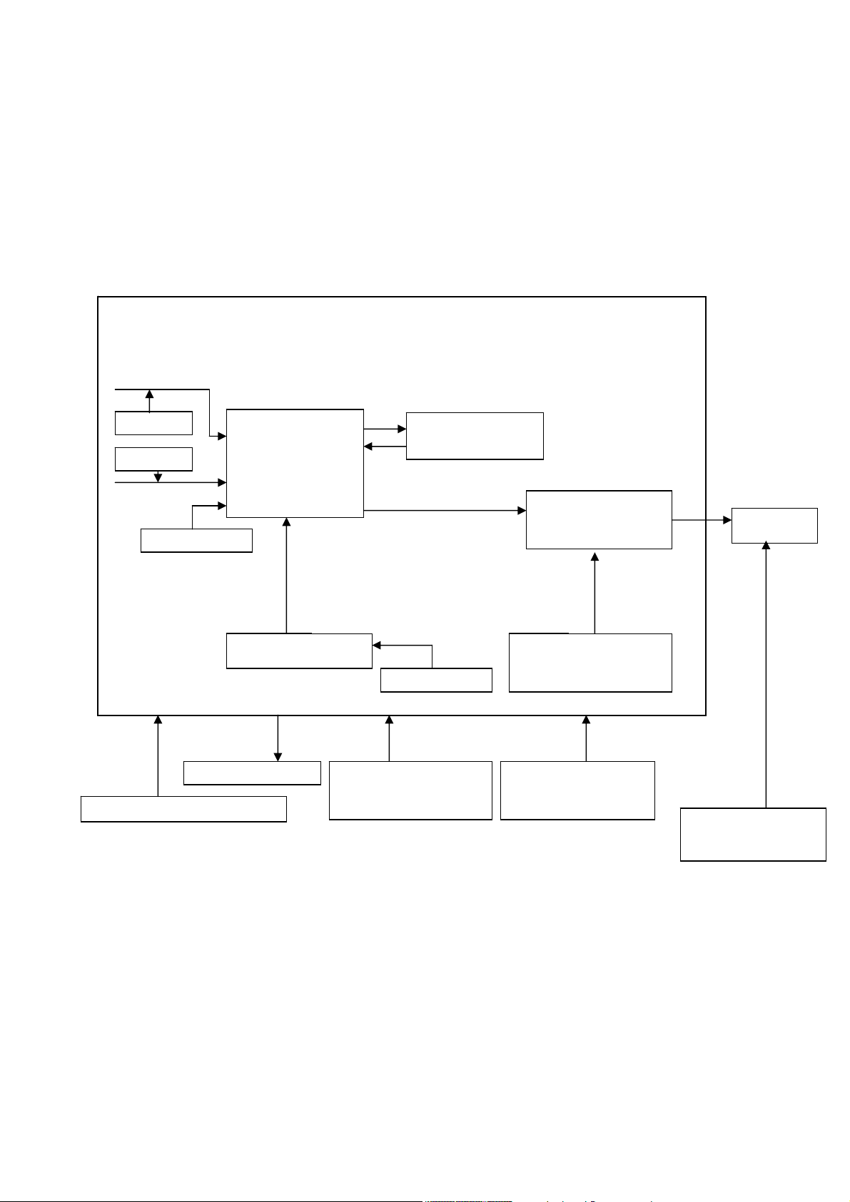
1-2 LCD MONITOR DESCRIPTION
p
Osc
The LCD monitor contains main-board, Inverter module, keyboard, audio module,
USB-hub module and External Adapter.
The main-board controls all logic signals such as panel control logic, backlight
control logic, …etc.
The Inverter module will drive the backlight of panel.
The Adapter supplies power to the LCD monitor.
Analog RGB
DDC-chip
-
DVI input
DC 12V 5Amp
illator 24
-
Gm5020 (U600)
MCU (U502)
Main-board Block diagram
Frame store
Data Digital RGB
Panel Control Signal:
Phs, Pvs, PclkA/B,
Pdis
e
Communication signal:
Hclk, Hfs, Hdata0
Crystal 24 MHz
Audio module
(optional)
LVDS chip
PANEL
Panel Power 5V
Panel-Power Control
(U203)
USB hub module
(optional)
INVERTER
module
3
Page 5
1-3 PANEL SPECIFICATION (AU EN02)
1-3-1 Panel Feature
- 19 inch Color TFT-LCD
- ALL input signals are 2 Channel LVDS interface compatible
- Supported the SXGA(H1280Pixel × V1024Lines) resolution
- By applying 16.7M colors (RGB 8 bit data)
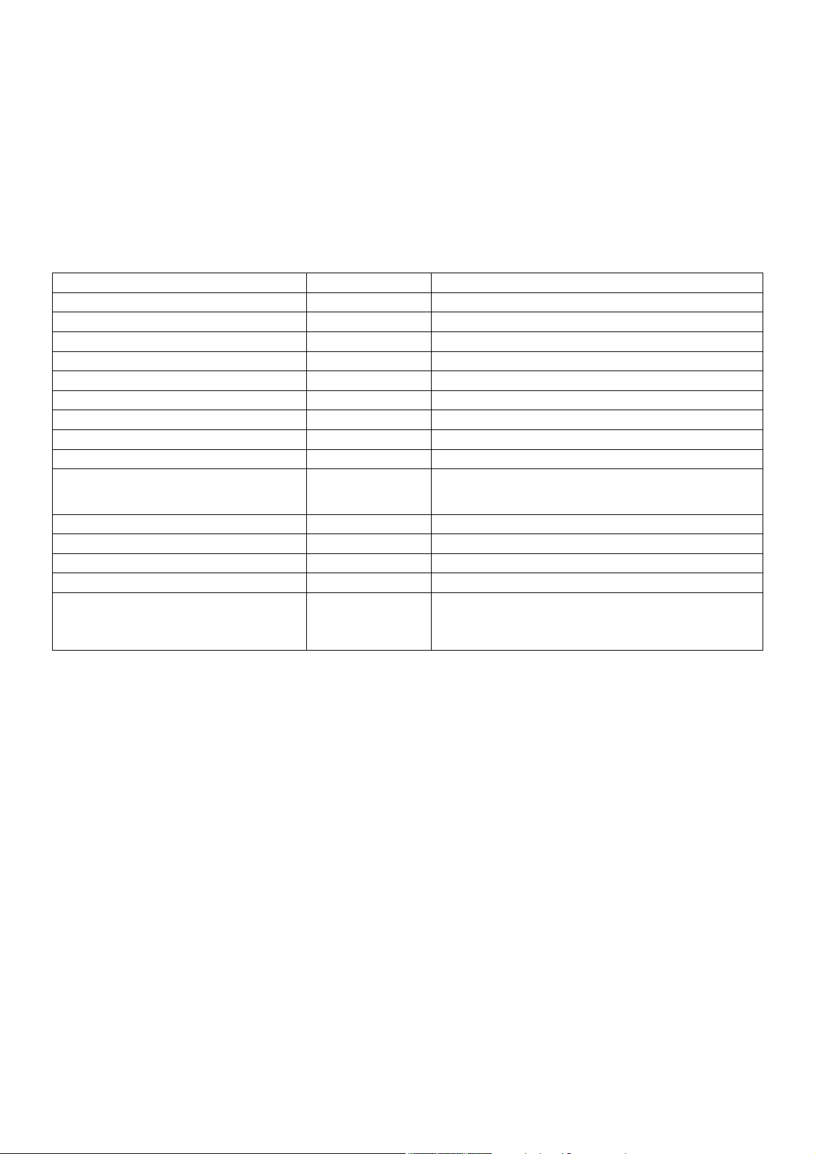
1-3-2 Display Characteristics
ITEM UNIT SPECIFICATIONS
Screen Diagonal [mm] 480(19”)
Active Area [mm] 376.32(H) x 301.056(V)
Pixel Pitch 1280(x3) x 1024
Pixel Arrangement [mm] 0.294(per one triad) x 0.294
Display Mode R.G.B Vertical Stripe
White Luminance (Center) [cd/m²] 250 cd/m²@7mA (Typ)
Contrast Ratio 600:1(Typ)
Optical Response Time [msec] 25(Typ)
Nominal input Voltage VDD [Volt] +5.0V
Power consumption
(VDD line + CCFL line)
[Watt]
28W (Typ.) (w/o Inverter, All white pattern)
Weight [Grams] 2700(Typ)
Physical Size [mm] 404.2(W) x330 (H) x20 (D)(Typ)
Electrical Interface Even/Odd R/G/B data, 3 sync signal Clock
Support Color 16.7M colors (RGB 8-bit data)
Temperature Range
Operating
Storage (Shopping)
[℃]
[℃]
0 to +50
-20 to +60
4
Page 6
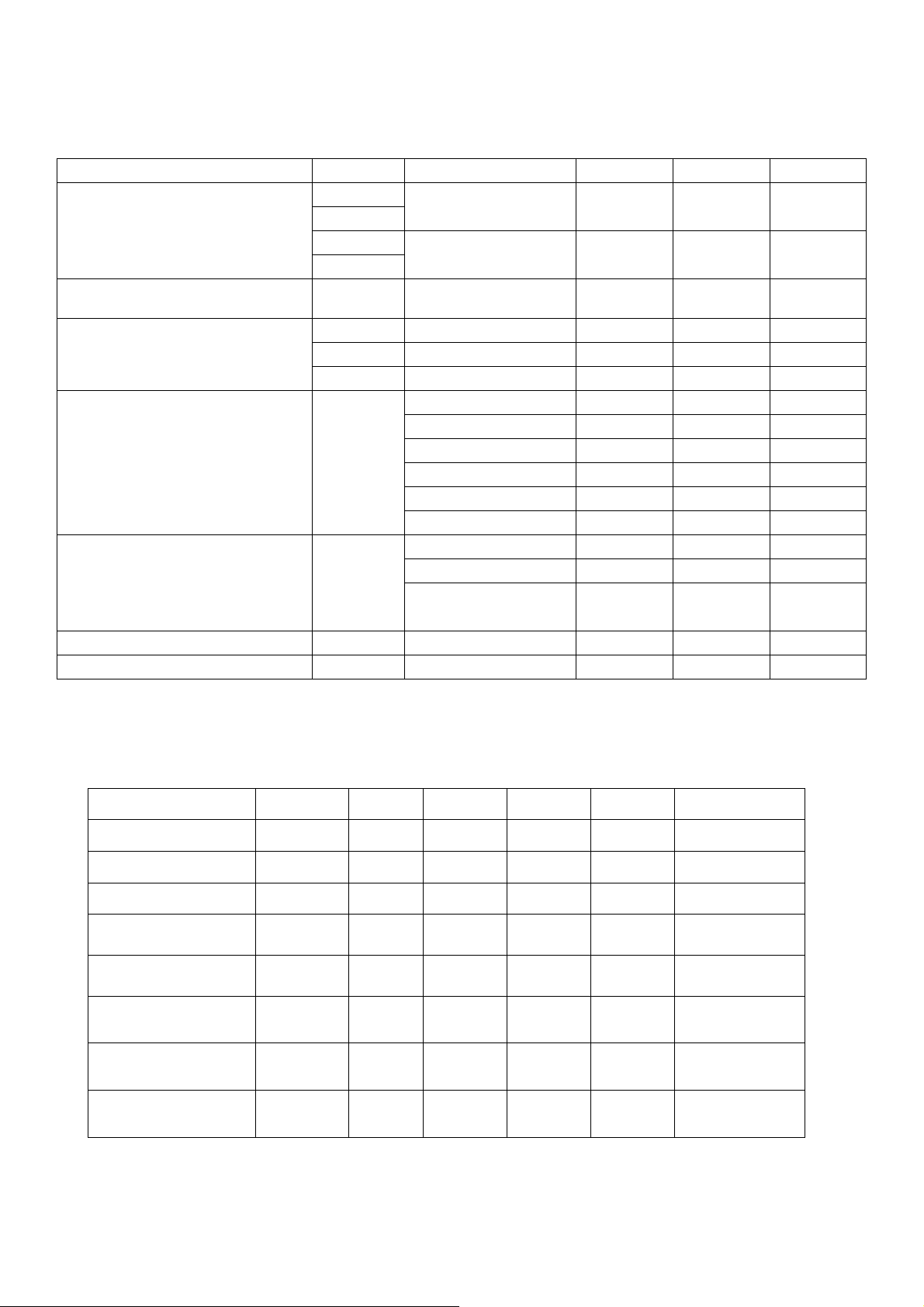
1-3-3 Optical Characteristics
The optical characteristics are measured under stable conditions at 25℃ (Room
Temperature):
ITEM UNIT CONDITIONS MIN TYP. MAX.
Viewing Angle
Contrast ratio Normal Direction 400 600
Response Time (Note 1)
Color Coordinates (CIE) White
White Luminance at CCFL
7.0mA
(central point)
[degree]
[degree]
[degree]
[degree]
[m sec] Raising Time – 15 25
[m sec] Falling Time – 10 15
[m sec] Raising +Falling – 25 40
[cd/㎡]
Horizontal (Right)
CR=10(Left)
Vertical (Up)
CR=10(Down)
Red x 0.604 0.634 0.664
Red y 0.324 0.354 0.384
Green x 0.278 0.308 0.338
Green y 0.576 0.606 0.636
Blue x 0.108 0.138 0.168
Blue y 0.057 0.087 0.117
White x 0.28 0.31 0.34
White y 0.3 0.33 0.36
200 250 –
75
75
85
85
85
85
–
–
–
–
Luminance Uniformity (Note 2) [%] 75 80 –
Crosstalk (in 75Hz)(Note 3) [%] 1.5
1-3-4 Parameter guide line for CCFL Inverter
INVERTER MAX BRINGTHNESS (Vadj: 3.0v), LOAD=100KΩX4(ROOM
TEMPERATURE 25℃ ±4℃)
ITEM SYMBOL MIN. TYP. MAX. UNIT REMARK
Input voltage Vin 10.8 12 13.2 V
Input current Iin --- 1950 2200 mA FOR 4 LOAD
Output Current Iout 6.0 7.0 8.0 mA FOR 1 LOAD
Frequency
H.V open Vopen 1550 1700 1850 Vrms NO LOAD
H.V Load Vload 620 670 720 Vrms RL=100KΩ
Start voltage Vst
F 45.0 50.0 55.0 KHZ
1870 1970 2070 Vrms RL=CCFL
FOR 1 LOAD
Protect delay time PDT
1 1.5 3 Sec
5
Page 7
INVERTER MIN BRINGTHNESS (Vadj:0.0v), LOAD=100KΩX4(ROOM
TEMPERATURE 25℃ ±4℃)
ITEM SYMBOL MIN. TYP. MAX. UNIT REMARK
input voltage Vin 10.8 12 13.2 V
input current Iin 470 520 mA FOR 4 LOAD
Output Current Iout 2.5 3.0 3.5 mA FOR 1 LOAD
Frequency
F 45.0 50.0 55.0 KHZ
FOR 1 LOAD
H.V open Vopen 1550 1700 1850 Vrms NO LOAD
Start voltage Vst
1650 1970 2050 Vrms RL=CCFL
H.V Load Vload 270 320 370 Vrms RL=100KΩ
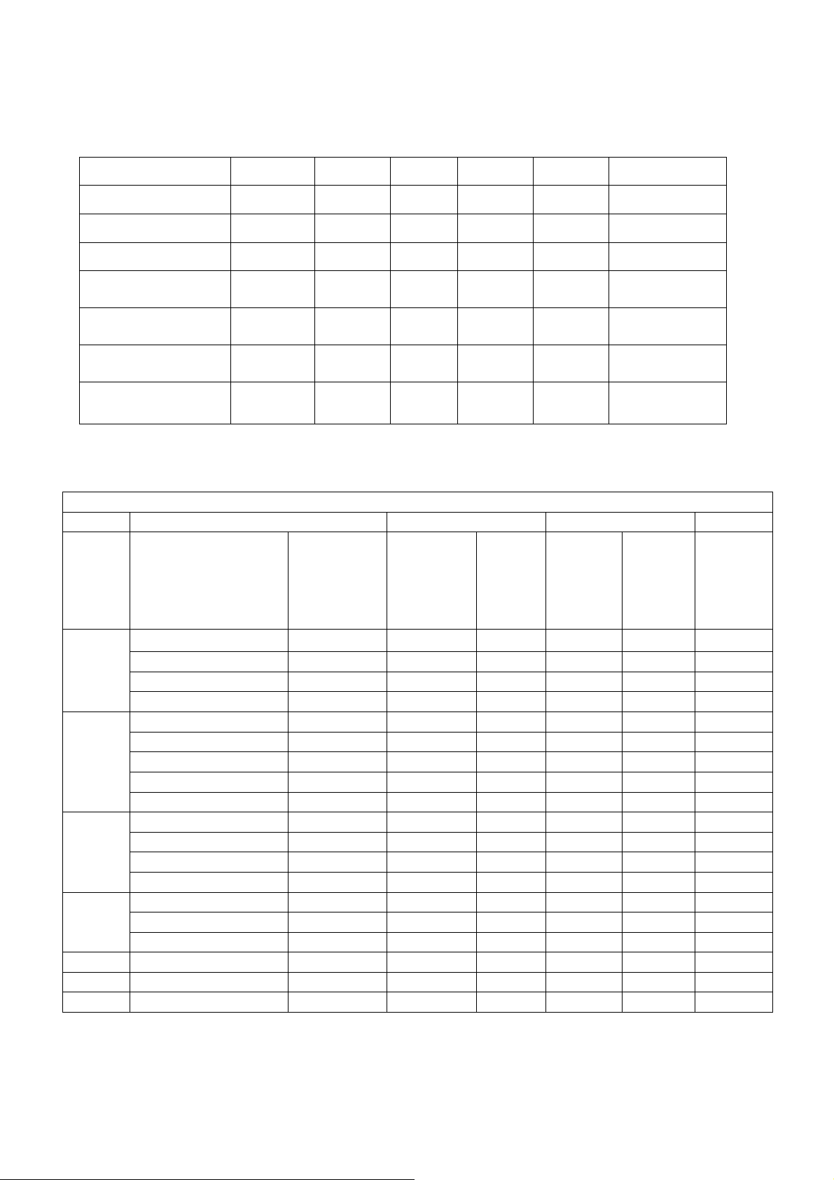
1-4 FACTORY PRESET TIMING LIST
VESA MODES
Horizontal Vertical
Nominal
Frequenc
Mode Resolution Total
y
+/-
0.5kHz
640x480@60Hz 800 x 525 31.469 N/P 59.940 N/P 25.175
VGA
640x480@72Hz 832 x 520 37.861 N/P 72.809 N/P 31.500
640x480@75Hz 840 x 500 37.500 N/P 75.00 N/P 31.500
640x480@85Hz 832 x 509 43.269 N/P 85.008 N/P 36.000
800x600@56Hz 1024 x 625 35.156 N/P 56.250 N/P 36.000
800x600@60Hz 1056 x 628 37.879 N/P 60.317 N/P 40.000
SVGA
800x600@72Hz 1040 x 666 48.077 N/P 72.188 N/P 50.000
800x600@75Hz 1056x 625 46.875 N/P 75.000 N/P 49.500
800x600@85Hz 1048x631 53.674 N/P 85.061 N/P 56.250
1024x768@60Hz 1344x806 48.363 N/P 60.004 N/P 65.000
XGA
1024x768@70Hz 1328x806 56.476 N/P 70.069 N/P 75.000
1024x768@75Hz 1312x800 60.023 N/P 75.029 N/P 78.750
1024x768@85Hz 1376x808 68.677 N/P 84.997 N/P 94.500
1280x1024@60Hz 1688x1066 63.981 N/P 60.020 N/P 108.000
SXGA
1280x1024@75Hz 1688x1066 79.976 N/P 75.025 N/P 135.000
1280x1024@85Hz 1728x1072 91.146 N/P 85.024 N/P 157.500
1152x 864@75Hz 1600x900 67.500 N/P 75.000 N/P 108.000
1280x960@60Hz 1800x1000 60.000 N/P 60.000 N/P 108.000
1280x960@85Hz 1728x1011 85.938 N/P 85.002 N/P 148.500
Notice: For digital input, the resolution 1280x1024@ 85hz, 1280x960@ 85Hz are not
supported.
Sync
Polarit
y
Nomina
l
Freq.
+/- 1 Hz
Sync
Polarity
Nominal
Pixel
Clock
(MHz)
6
Page 8
IBM MODES
Horizontal Vertical
Nominal
Pixel
Clock
(MHz)
Mode Resolution Total
Nominal
Frequency
+/- 0.5kHz
Sync
Polari
ty
Nominal
Freq.
+/- 1 Hz
Sync
Polarit
y
DOS 720x400@70Hz 900 x 449 31.469 N 70.087 P 28.322
720x400@85Hz 936 x 446 37.927 N 85.039 P 35.550
DOS 640x400@70Hz 800 x 449 31.469 N 70.087 P 25.175
DOS 640x350@70Hz 800 x 449 31.469 P 70.087 N 25.175
MAC MODES
VGA
640x480@67Hz 864x525 35.000 N/P 66.667 N/P 30.240
SVGA
832x624@75Hz 1152x667 49.725 N/P 74.551 N/P 57.283
All modes will automatically optimize the screen size with “ AUTO-config “ function, except
3 dos- modes: 640x480@60hz, 720 x 400@70hz, 640x350@70hz.
1-5 INTERFACE CONNECTION
(A) AC-Power Cable
(B) Video Signal Connectors and Cable
(C) DVI-D and DVI cable
(D) Audio cable (optional)
(E) USB cable (optional)
(F) External Adapter
7
Page 9

2. PRECAUTIONS AND NOTICES
2-1 ASSEMBLY PRECAUTION
(1) Please do not press or scratch LCD panel surface with anything hard. And do not
soil LCD panel surface by touching with bare hands (Polarizer film, surface of
LCD panel is easy to be flawed)
In the LCD panel, the gap between two glass plates is kept perfectly even to
maintain display characteristic and reliability. If this panel is subject to hard
pressing, the following occurs:
(a) Uniform color
(b) Orientation of liquid crystal becomes disorder
(2) Please wipe out LCD panel surface with absorbent cotton or soft cloth in case of
it being soiled.
(3) Please wipe out drops of adhesive like saliva and water in LCD panel surface
immediately.
They might damage to cause panel surface variation and color change.
(4) Do not apply any strong mechanical shock to the LCD panel.
2-2 OPERATING PRECAUTIONS
(1) Please be sure to unplug the power cord before remove the back-cover. (Be sure
the power is turn-off)
(2) Please consider that LCD backlight takes longer time to become stable of
radiation characteristic in low temperature than in room temperature.
(3) Please pay attention not to displaying the same pattern for very long-time. For
image might stick on LCD.
2-3 STORAGE PRECAUTIONS
(1) When you store LCD for a long time, it is recommended to keep the temperature
between 5℃-40℃ without the exposure of sunlight and to keep the humidity less
than 85% RH.
(2) Please do not leave the LCD in the environment of high humidity and high
temperature such as 60℃ 90%RH.
(3) Please do not leave the LCD in the environment of low temperature; below -15℃.
2-4 HIGH VOLTAGE WARNING
The high voltage is only generated by INVERTER module; carelessly contacting the
transformer on this module can cause a serious shock. (The lamp voltage after
stable around 600V, with lamp current around 6.5mA, and the lamp starting voltage
was around 1650V, at Ta=25℃)
8
Page 10
3. OPERATING INSTRUCTIONS
This procedure gives you instructions for installing and using the LCD monitor
display.
1. Position the display on the desired operation and plug–in the power cord into
External Adapter AC outlet. Three-wire power cord must be shielded and is
provided as a safety precaution as it connects the chassis and cabinet to the
electrical conduct ground. If the AC outlet in your location does not have
provisions for the grounded type plug, the installer should attach the proper
adapter to ensure a safe ground potential.
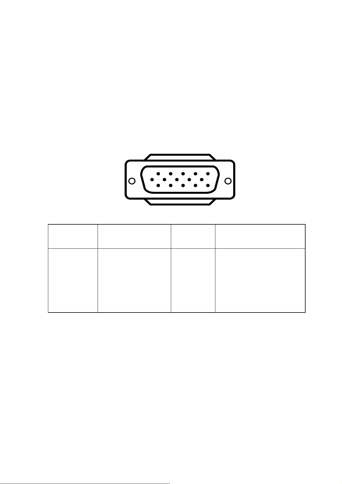
2. Connect the 15-pin color display shielded signal cable to your signal system
device and lock both screws on the connector to ensure firm grounding. The
connector information is as follow:
15 - Pin Color Display Signal Cable
PIN NO.
DESCRIPTION
1. RED 9. 5V power from VGA-card
2. GREEN 10. Detect Cable
3. BLUE 11. SYNC. GND
4. GND 12. DDC-Serial Data
5. GND 13. HORIZ. SYNC
6. GND-R 14. VERT. SYNC
7. GND-G 15. DDC Serial Data
8. GND-B
1
6
11 15
PIN NO.
5
10
DESCRIPTION
9
Page 11
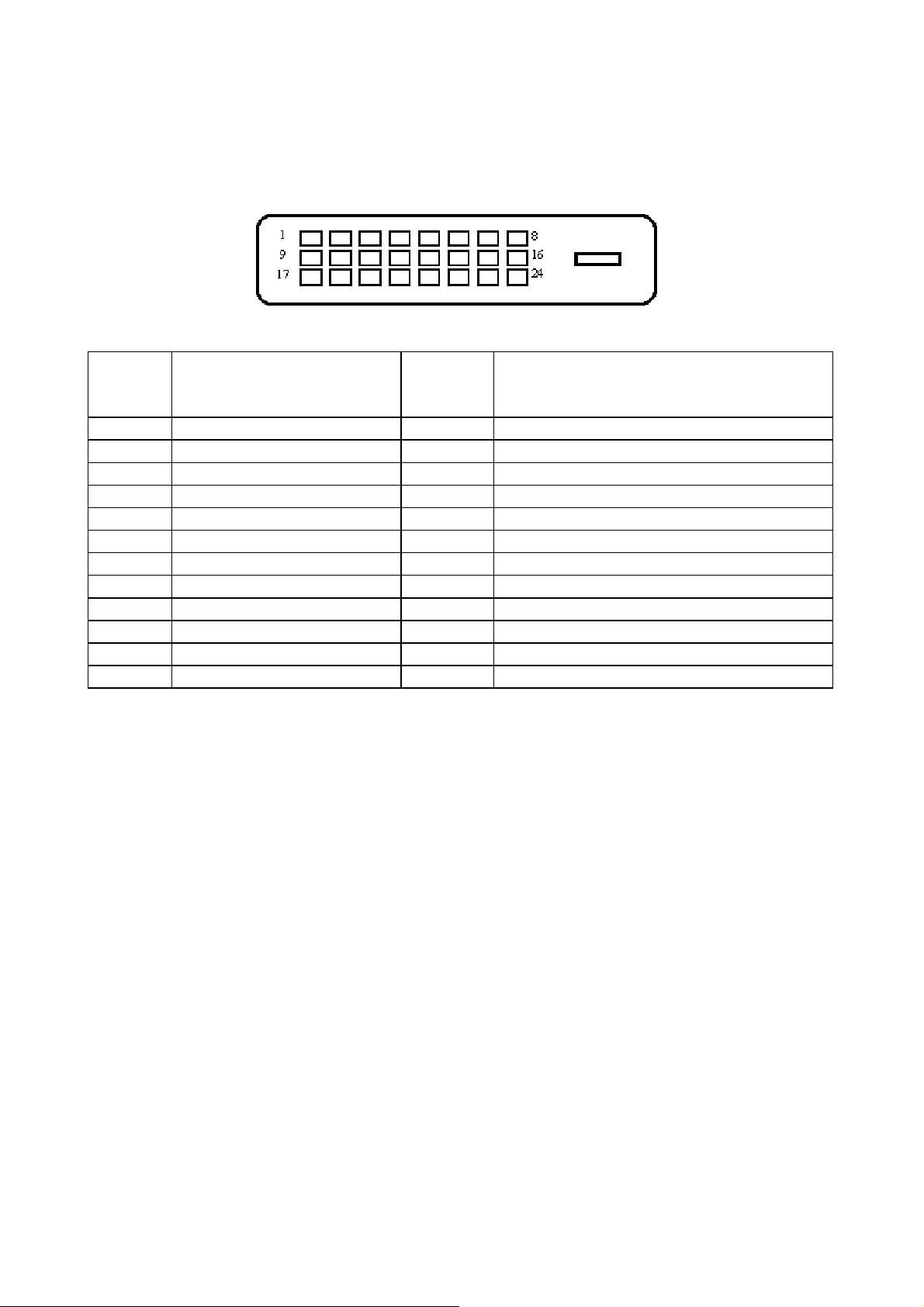
3. Connect the 24-pin color display shielded DVI-DVI signal cable to your signal
system device and lock both screws on the connector to ensure firm grounding.
The connector information is as follow:
15 - Pin Color Display Signal Cable
PIN NO.
DESCRIPTION
PI N NO.
DESCRIPTION
1. TMDS Data 2- 13. TMDS Data 3+
2. TMDS Data 2+ 14. +5V Power
3. TMDS Data 2/4 Shield 15. Ground (for+5V)
4. TMDS Data 4- 16. Hot Plug Detect
5. TMDS Data 4+ 17. TMDS Data 0-
6. DDC Clock 18. TMDS Data 0+
7. DDC Data 19. TMDS Data 0/5 Shield
8. N.C. 20. TMDS Data 5-
9. TMDS Data 1- 21. TMDS Data 5+
10. TMDS Data 1+ 22. TMDS Clock Shield
11. TMDS Data 1/3 Shield 23. TMDS Clock +
12. TMDS Data 3- 24. TMDS Clock -
4. Apply power to the display by pressing the power key for about 2 second
consecutively and allow about several seconds for Panel warm-up. The PowerOn indicator lights up when the display is on.
5. With proper signals feed to the display, a pattern or data should appear on the
screen, adjust the brightness and contrast to the most pleasing display, or press
auto-key to get the factory preset best picture-quality.
6. This monitor has power saving function following the VESA DPMS. Be sure to
connect the signal cable to the PC.
7. If your LCD monitor requires service, it must be returned with the power cord &
Adapter.
10
Page 12

4. ADJUSTMENT
4-1 ADJUSTMENT CONDITIONS AND PRECAUTIONS
Adjustments should be undertaken only on following function: Contras, Brightness,
Black level, Phase, Clock, H/V-position, Languages, Color- (C2, C1, User), Auto level, ,
Languages, Reset, RGB level, input selected, scaling mode
- Power Button:
When pressed, the monitor enters the off mode, and the LED turns blank. Press again
to restore normal status.
- Left / Right Button:
The Left/Right Button is used to control the monitor functions. Press to switch
functions or adjust settings.
- Auto Adjust Key:
The Auto Adjust Key is used to automatically set the H Position, V Position, Clock and
Phase.
- Power Indicator:
Green — Power On mode.
orange — Power Saving mode.
Blank —Power Off Mode.
4-2 ADJUSTMENT METHOD AND DESCRIPTION
4-2-1 White-Balance, Luminance adjustment
Approximately 30 minutes should be allowed for warm up before proceeding white
balance adjustment.
Before start adjusting white balance, please set Chroma-7120 MEM. Channel 1 to C2
color and MEM. channel 2 to C1 color, (our C2 parameter is x = 296 ±20, y = 311 ±20,
Y = 220 and C1 parameter is x = 313 ±20, y = 329 ±20, Y = 220)
How to setting MEM. channel you can reference to chroma 7120 user guide or simple
use “ SC” key and “ NEXT” key to modify x,y,Y value and use “ID” key to modify the
TEXT description
Following is the procedure to do white-balance adjustment:
Press MENU button during 1 seconds along with plug in the DC-power cord will
activate the factory mode, and the OSD screen will located at left top of the panel.
Alignment Procedure
1.) Pattern generator Output: Timing 1280x1024@60hz, Pattern 32 Gray Scale, Analog.
2.) Connect Alignment Tool JP2 with Chroma 7120, JP3 with Monitor Analog
Connector, JP4 with Pattern Generator.
3.) Press Menu and Select Button, then Power on Monitor to enter Factor Mode.
4.) Press [SW1] at Alignment Tool.
5.) Change Pattern Generator Pattern to Full White Pattern.
6.) Press [SW2] at Alignment Tool.
7.) Wait LED from OK -> BUSY -> OK.
8.) Press [SW3] once to verify 7800 color temperature.
9.) Press [SW3] once to verify 6500 color temperature.
10.) If there is error at step 7 to 8, repeat step 4 to 9.
4-2-2 OSD adjustments
11
Page 13

Turn the POWER-button off to on to quit from factory mode (in USER-mode, the
OSD window location was placed at the middle of the screen) Press MENU
button to activate OSD Menu or make a confirmation on desired function, Press
Left/Right button to select the function or done the adjustment.
1. Clock adjustment
Set the Chroma at pattern 63 (cross-talk pattern) or WIN98/95 shutdown mode
(dot-pattern).
Adjust until the vertical-Stripe-shadow as wide as possible or no visible.
This function is adjust the PLL divider of ADC to generate an accurate pixel clock
Example: Hsyn = 31.5KHz Pixel freq. = 25.175MHz (from VESA spec)
The Divider number is (N) = (Pixel freq. x 1000)/Hsyn
From this formula, we get the Divider number, if we fill this number in ADC
register (divider register), the PLL of ADC will generate a clock which have same
period with above Pixel freq. (25.175MHz) the accuracy of this clock will effect the
size of screen. (This clock was called PIXEL-CLOCK)
2. Focus adjustment
Set the Chroma at pattern 63 (cross talk pattern) or WIN98/95 shut down mode
(dot-pattern).
Adjust the horizontal interference as less as possible
This function is adjusting the phase shift of PIXEL-CLOCK to acquire the right
pixel data.
If the relationship of pixel data and pixel clock not so match, we will see the
horizontal interference on screen, we only find this phenomena in crosstalk
pattern or dot pattern, other pattern the affect is very light
3. H/V-Position adjustment
Set the Chroma to pattern 1 (crosshatch pattern) or WIN98/95 full-white pattern
confirm above item 2 & 3 functions (clock & focus) was done well, if that 2
functions failed, the H/V position will be failed too. Adjust the four edges until all
four-edges are visible at the edge of screen.
4. Language function
There have 5 languages for selection, presses “MENU” to select and confirm,
press “UP” or “ DOWN” to change the kind of language (English, Deutch,
Francais, Espanol, Italian)
5. Reset function
Clear each old status of auto-configuration and re-do auto-configuration (for all
mode)
This function also recalls C2 color-temperature.
The descriptions for function control LEDS is as following list
12
Page 14
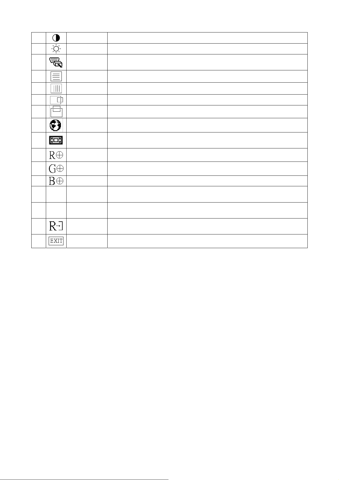
1.
2.
3.
Contrast Adjust the picture contrast.
Brightness Adjust the picture brightness.
Input
Selected
Input Signal source selected (select Analog or Digital input
source)
4.
5.
6.
7.
8.
9.
10.
11.
12.
13 C1
15. C2
16.
17.
Focus Adjust picture Focus.
Clock Adjust picture Clock.
H- Position Adjust the horizontal position of the picture.
V- Position Adjust the vertical position of the picture.
Language Multi-Language selection
Scaling
Mode
Red Adjusts Red intensity.
Green Adjusts Green intensity.
Blue Adjusts Blue intensity.
(6500K)
Color
(7800K)
Color
Reset
Exit Save user adjustment and OSD disappear.
Stretch the picture to fit full screen, screen size ratio or native
size.
The color temperature for 6500°K is x=0.313, y=0.329.
The color temperature for 7800°K is x=0.296, y=0.311.
Clear each old status of Auto-configuration and re-do auto-
configuration and set the color temperature to 7800°K.
13
Page 15

555 55 BLOCK DIAGRAM
6655-1 SPECIAL FUNCTION WITH PRESS-KEY
Press menu button during 2 seconds along with plug-in the DC Power cord:
That operation will set the monitor into “Factory- mode”, in Factory mode we can
do the White balance adjustment with RS232 .In Factory mode, OSD-screen will
locate in left top of screen. Press POWER-button off to on once will quit from
factory mode and back touser-mode. The OSD-index explanation is as following:
1. No signal: No signal input (Signal-cable not connected).
2. Input not supported:
a. Input frequency out of range: H > 92kHz, v > 85Hz or H < 31kHz, v < 55Hz
b. Input frequency out of VESA-spec. (Out of tolerance too far)
5-2 CIRCUIT FUNCTION DESCRIPTION
5-2-1 main board
1. U600, scaler IC gm5020 (all-in-one chip solution for ADC, OSD, scalar and
interpolation):
USE for computer graphics images to convert analog RGB data to digital data with
interpolation process, zooming, generated the OSD font, perform overlay function
and generate drive timing for LCD-PANEL.
2. U502, W78E65 (WINBOND- MCU, type 8052 series with 64k Rom-size and 512
byte ram):
Use for calculate frequency, pixel-dot, detect change mode, rs232-communication,
power-consumption control, OSD-index warning, …etc.
3. U301,ATMEL12524C02N
EEPROM type, 1K ROM-SIZE, for saving Digital DDC-CONTENT.
4. U302, MIRCOCHIP24LC21A
EEPROM type, 1K ROM-SIZE, for saving Analog DDC-CONTENT.
4. U501, 24C16 (ATMEL IC):
EEPROM type, 16K ROM-SIZE, for saving AUTO-config data, White-balance data,
and Power-key status and Backlight-counter data.
5. U901,SI8050(switching regulator 12V to 5V with 3A load current) .
6. U904,AIC 1084-33CM (AIC brand linear regulator 5V to 3.3V)
7. U902,RT9164(Linear regulator 5V to 2.5V)
8. U201,U202,LVDS ( use NOVATEK NT7181F)
Convert the TTL signal to LVDS signal , the advantage of LVDS signal is : the
wire can be lengthen and eliminate wire number , low EMI .LVDS signal is high
frequency but low voltage, only 0.35 VPP ,the frequency is seven times higher than
TTL
14
Page 16
5-2-2 adapter/inverter
1. ADAPTER: CONVERSION-module to convert AC 110V-240V to 12VDC, with 5
AMP
2. INVERTER: CONVERSION-module to convert DC 12V to High-Voltage around
1650V, with frequency 30K-80Khz, 5mA-13mA
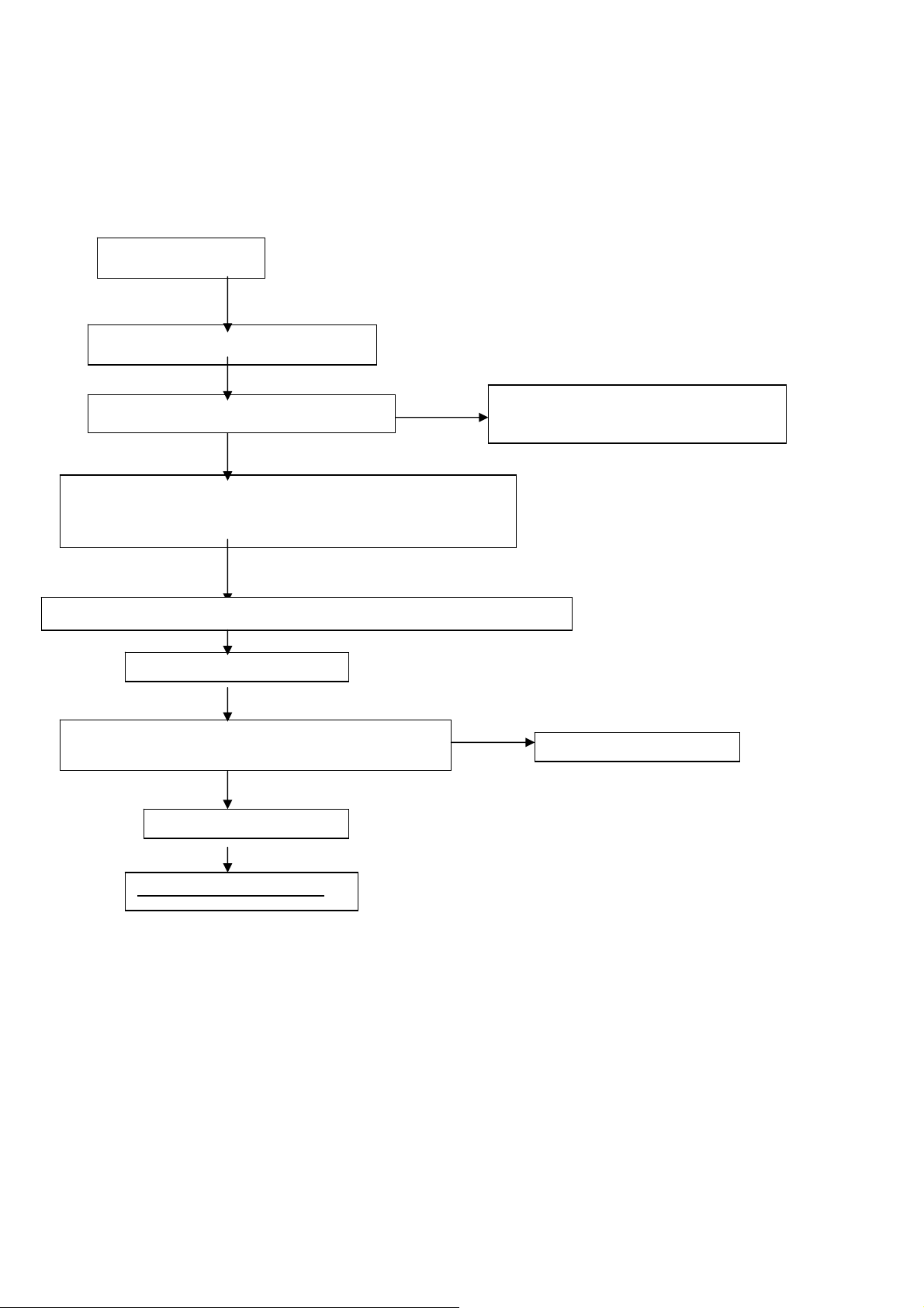
5-3 SOFTWARE FLOW CHART
POWER-ON START
Initial MCU I/O, Interrupt vector & Ram
Check Eeprom is empty?
Check White-balance data (C1 & C2) same with the backup data?
Check POC (backlight counter) data same with the backup data?
IF not same, overwrite the data with backup value.
Check Previous power-switch status from Eeprom, & other system status
Initial gm5020
Check if in Factory mode? (When power-on, press the
MENU Button will be in FACTORY mode)
Clear factory mode flag
MAIN-SUBROTINE LOOP
Initial 1.POC (backlight counter)
2. Clr all mode value
SET factory mode flag
15
Page 17
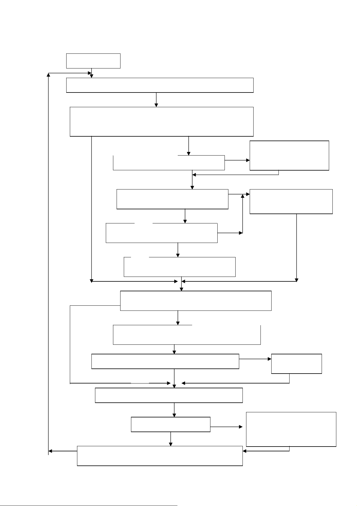
Main subroutine loop
Main loop start
Process Power-saving status (according to below flow-chart result)
Check gm5020 IFM status .is change or not.
And check Signal cable status (cable not connected or not)
** IFM is the register, which measured the HSYN & Vsyn status
Check the IFM result is in the user mode
table?
Check Auto-config mode flag already been set?
Read Key status and Process on OSD-screen
Monitoring the time-out of osd status (if no key input persist for
10 sec, the osd time-out counter will trigger)
)
Yes, IFM have change
Is current system status in Power-saving?
Check the IFM result is in the standard
Mode table?
Out of range (input not support) be
confirm
Confirm the frequency (Hsyn or Vsyn) from IFM already
been changed? (Check the change mode flag)
Process (turn off OSD, setting GM5020according to
above parameter, set LED status, set backlight status)
Check Factory mode flag= 1
Wake-up gm5020
(Because gm5020 was in
partial sleeping state)
Set mode index & parameter
Set change mode flag
Do Auto-config
automatically
If the RS232 buffer is full,
process the command (while
adjust white-balance in factory
mode)
16
Page 18

6.MAINTAINABLITY
6-1. EQUITMENTS AND TOOLS REQUIRED
1.) Voltmeter.
2.) Oscilloscope.
3) Pattern Generator.
4) DDC Tool with a personal computer
5) Alignment Tool.
6) LCD Color Analyzer.
7) Service Manual.
8)User Manual.
6-2 TROUBLE SHOOTING
6-2-1 interface board trouble shooting chart
*Use the PC Win 98 white pattern, with some icon on it, and Change the Resolution to
640x480 60 Hz / 31 KHz
**NOTICE: The free-running freq. of our system is 48 KHz / 60 Hz, so we recommend to
use another resolution to do trouble shooting, this trouble shooting is proceed with
640x480 @60Hz 31Khz
17
Page 19

g
k
K
,
K
,
I. No screen appear
No
Measured Input DC-voltage (J1)= 12 V?
Measured U901 SI-8050 pin4=5V?
Measured U904 AIC 1084 pin 2 = 3.3V?
Measured U903 AIC1117 pin 2= 3.3V?
Measured U902 RT9164 pin 2=2.5v
Measured U905 AIC 1084 pin2=2.5V
DC-Power Part
Check Correspondent component.
Is there any shortage or cold solder?
Disconnected the Signal cable (Loose the
Signal cable), Is the screen show “No
”
No, nothing is show
Connected the Signal cable again,
Check LED status.
Check the Wire-Harness from CN201
Was tight enough?
Check the Wire connection to panel side too
Led Green
Yes, all DC level exist
Led Orange
OK, Keyboard no stuc
Connected the Signal cable again,
Check LED status.
Check Power switch is in Power-on
status, and check if Power switch had
been stuck?
Led orange
Measured RGB (r302, r304, r306) H, V Input at
nal input pin13, 15 was there signal?
si
NG
O
OK, Wire tight
Check Panel-Power Circuit Block
input
Measured Oscillator Block
Crystal X501
Check U600 Data-output Block
OK, Panel Power OK
O
clock
Check communication pin between U600 &
MCU pin 2,6,7. , Is it have transition?
OK, U600 data OK
OK, Mcu have transition
NG, no transition
Replace Inverter and Check
Inverter control relative circuit
Re-do White balance adjust
Replace U600 (Gm5020)
Replace U502 (MCU)
& Check Reset pin 10
Must be change from High to
low when first AC power plugin
OK
OK
Note: 1. If Replace “Main board”, Please re-do“DDC-content”programmed & “White-balance”.
2. If Replace “ Inverter” only, Please re-do “ White-Balance”
Led Green
Replace MCU
Check Correspondent
component short/open
(Protection Diode)
and Signal cable bad?
18
Page 20

PANEL-POWER CIRCUIT
p
OK, & Re
Check U
Check R202 should have response from 0V to 5V
When we switch the power switch from off to on
Measured the U203 pin 5,6,7,8= 5 V?
OK
INVERTER Control Relative Circuit
Measured the inverter connector CN502
Pin 1,2=12V, pin 3 on/off control=5V (on)
Replace INVERTER to new-one, and
Check the screen is normal??
OSCILLATOR BLOCK
Measured X501 Oscillator output 24MhZ?
Measured X600 Crystal output 24 KHz?
OK, R202 have
-do white
OK
NG, no Voltage
U600-DATA OUTPUT
Measured DCLK, DHS, DVS, DEN (pin G20,
F20, F19, F18 from U600)
Is there have any transition?
Pclk around 47MHz to 57MHZ, PVS=60.09Hz,
PHS around 67 KHz?? (Refer to input
signal=640x480@60 Hz 31k, and LED is green)
OK
Check the PPWR panel power relative circuit,
R201, R202, Q201, U203 (pin 5,6,7,8)
In normal operation, when LED =green, R223
Should =0 v,
If PPWR no-response when the power switch
Turn on and turn off, replace the U600-GM5020
Check U203 pin 1,3= 5V
Replace U203 (Nmos, SI9953)
NG
502 pin18
Check the Bklt-On relative circuit, R520, Q503, R519,
In normal operation, when LED =green,
R520 Bklt-On should =0 v,
If Bklt-On no-response when the power switch turn on-off,
Re
lace the MCU
Replace Oscillator X501
Replace Crystal X300
Replace GM5020 (U600) or replace
main board
If Main Board being replace, please
do the DDC – content
19
Page 21

p
II (a) the screen is abnormal, stuck at white screen, OSD window can’t appear,
but keyboard & LED is normal operation.
At general, this symptom is cause by missing panel data or panel power, so we must
check our wire-harness, which connected to panel or the panel power controller (U203)
Check if the Wire harness from CN201 loose?
Check the wire on both Panel-side and Main board side.
Tighten it.
Yes, tight enough
Check the Panel-Power circuit as above (page 20)
U203 pin 5,6,7,8, must be 5V
Yes, Voltage normal
Check the LVDS-Power L904= 3.3V?
Yes, Voltage normal
Check both U201 & U202 LVDS-Input pin 31= 45mhz –
65mhz, and pin 28 = Vsyn freq, pin 27 = 45khz- 65 kHz
Yes, Frequency normal
Replace both LVDS chip (U601 & U602)
Check U903, which convert the 5V to
3.3V
Check U600 DATA-OUPUT block as
above (page 20)
NG, no data output
Check OSCILLATOR Block as
above (page 20)
OK, all clock is normal
Replace U502 MCU and check it RESET
pin 10, must be turn high to low when first
AC
ower-on
OK, reset is normal
Check U600 DATA-OUTPUT block again
NG, still no data out
Replace U600 GM5020
20
Page 22

II. (B) The screen had the Vertical Straight Line, may be stuck in Red, Green or Blue
That symptom is cause by bad Panel issue (might be the Source IC from Panel is cold
soldered or open looped) so replace the panel and try it.
III.ALL SCREEN HAS INTERFERENCES OR NOISE, CAN’T BE FIXED BY AUTO KEY
** NOTE: There are so many kinds of interferences,
1). One is caused by some VGA-CARD that not meet VESA spec or power grounding too
bad that influence the circuit.
2). Other is cause by external interferences, move the monitor far from electronic
equipment. (Rarely happened)
Use DOT-pattern, or win98/99 shutdown
mode pattern, press “AUTO” key, was the
interferences disappear??
Adjust “FOCUS” step by step, until the
horizontal interferences disappear
Does your signal-cable have an additional
cable for extension??
Does your noise only exist in one mode only?
(Ex: only at 1280x1024 @ 85 Hz, other is normal)
That was caused by you VGA-CARD setting, your VGA
card timing back porch / front porch exceed vesa timing
too far, for some new AGP-VGA-CARD such situation
always happened
So in your control-panel icon, select monitor, setting,
advance, screen-adjust, at
Size icon, increase step by step slowly, and press,
“AUTO” key every step you increase the SIZE repeat
the procedure (increase/decrease SIZE one-step and press
AUTO) until the interferences disappear, press
“APPLY” to save in your VGA
No additional extension cable
Yes, only happened on one mode
Yes, has extension
END
END
Put away the additional cable
May be the additional cable grounding is
not quite good.
Change the Signal-cable to new one or
Try other brand VGA-CARD
(Make sure just only that brand VGACARD has this problem)
21
Page 23

III There is interferences in DOS mode
NOTE: the criteria of doing AUTO-CONFIGURATION: must be a full-size screen, if the
screen not full, the auto-configuration will fail. So in DOS mode, just set your “CLOCK” in
OSD-MENU to zero or use some EDITOR software which can full fill the whole screen (ex:
PE2, HE) and then press “AUTO” Or you can use “DOS1.EXE” which attached in your
Driver disk to optimize DOS mode performance.
IV The panel luminance is down
Use white pattern and resolution 1280x1024 @ 60Hz, CHROMA 7120 measured the
center of panel
Set Contrast, brightness =maximal, RGB= 50
Quit from OSD-screen, measured Y (luminance)
With chroma 7120, check Y= 230±10 cd/m2?
If Y can reach >240 cd/m2 that means
The lamp still working well, so we just re-do the
white-balance process
As following procedure
If the Y less than 200 cd/m2 (after the contrast,
brightness = max) then change the LAMP of panel
Use white-pattern, press MENU button along
with AC power-plug in (you will in factory
mode) The OSD-menu will be at left top of
screen,
Press AUTO button to automatically adjust black
level value, you will see the sign PASS
Follow White-Balance, Luminance adjustment
as above, method to more detail procedure
For do a white-balance adjust
6-2-2 INVERTER –MODULE TROUBLE SHOOTING CHART
**Note: the Waveform of U901 pin 2 can determined the power situation
1. Stable rectangle waveform with equal duty, freq around 150K-158KHz
that means all power of this interface board is in normal operation
, And all status of 5V & 3.3V is working well
2. Unstable or uneven rectangle waveform without same duty, that means
ABNORMAL operation was happened, check 3.3V or 5V, if short-circuit or bad
component
3. Rectangle waveform with large spike & harmonic pulse on front side means all
3.3v is no load, U600 Gm5020 was shut-down, and only U502 MCU still working,
that means the monitor is in power saving status, all power system is working
well.
22
Page 24

Check IC1 pin9=12V
pin9=12vvoltage of
C905(+)
Check C1 (+) =12V
NG
OK
Check ON/OFF signal
NG
OK
NG
Check the pin1 of IC1 have saw tooth wave
OK
Check F1/ D1/Q3/Q4or
D2/Q9/Q10
Check Interface board
CheckQ1 or Q2
OK
NG
Change IC1
Check MOSFET Q5/Q8 if has the output of square wave.
OK
NG
Check Q6/Q7//D3 or
Q11/Q12 /D4
Check the resonant wave of pin2 & pin5 for T1/T2
OK
NG
Check Q6/Q7/C5 or
Q11/Q12/C19
Check the output of T1/T2
OK
NG
Change T1or T2
Check connecter & lamp
END
23
Page 25

6-2-3 KeyPad Board module trouble-shooting chart
I
OSD is unstable or not working
Is KeyPad Board connecting normally?
Y
Is Button Switch normally?
Y
Is KeyPad Board Normally?
Y
N
N
N
Connect KeyPad Board
Replace Button Switch
Replace KeyPad Board
Check Main Board
24
Page 26

,
r
II
Check U502 MCU pin 43,42,41,40,39 at
High state (5V)? without press any key
Press power key and check U502 pin 43
= low (0V)?
Check U502 pin 37 (LED green) will have
transition from hi to low or low to hi when we
press the power key??
Check U502 pin 20= 24MHz? And pin 44
(VDD)=5V? And pin 10 (reset)=0V ? At norm al
condition
Without press key and change mode, Check U502
pin 16,17(SDA, SCL)= hi 5V? Or keep
transition?
Replace U502 MCU
NG, MCU no response
NG
Mechanical stuck, Check!
Check main board PR505 shortage?
Replace Tact-switch SW105 at keyboard if still
no work replace U302 MCU at main-board and
check MCU relative reset circuit, and crystal
If still no Led green indicator, check LED at
keyboard !! cold solder or bad
If one of these items was NG, check the relative
circuit
Keep transition that means eeprom no response
Check U501 eeprom 24LC16 relative circuit,
check U600 pin 7 = low?
Check the relative
power circuit, was
there 5v input
Check U501 pin 8
(vdd)= 5V, and check
R501
R503 cold solde
Replace eeprom
OK
25
Page 27

7.MECHANICAL OF CABINET FRONT DIS-ASSEMBLY
26
Page 28

8.POWER SYSTEM AND CONSUMPTION CURRENT
(
(
(
)
)
ADAPTER MODULE
Input AC 110V, 60Hz/240V, 50Hz
Output DC 12V 5A
SI-8050SD, 12V to 5V (5A SPEC)
5V
AIC1084
5V to 3.3V
5A SPEC)
3.3V
For GM5020 and
USB hub consumption
Main board power system
To CPU, Eeprom, 24c21, control-inverter-on.off,
and USB hub
860mA when Cable not connected
841mA when Normal operation
AIC1084
5V to 2.5V
800mA SPEC
2.5V
2.5V
For GM5020
Consumption
INVERTER MODULE
Input DC 12V
Output AC 1500V/30K-80KHz
Current 14mA
RT9164
5V to 2.5V
(1000mA
SPEC
For gm5020
consumption
AIC1117
5V to 3.3V
800mAspec)
3.3V
For LVDS consumption
27
Page 29
9. MAIN BOARD SCHEMATIC
Page 30

Sheet 3
3.Input Connectors
Sheet 4
HDATAF[0..3]
RED+
GREEN+
GREEN-
BLUE+
BLUE-
RXC+
RXCRX2+
RX1+
RX0+
DDC_SCL
DDC_SDA
/RESET
GPIO[0..7]
HCLK
/PANEL_EN
LVDS_EN
RED-
RX2-
RX1-
RX0-
HFS
/IRQ
Sheet 5
RED+
REDGREEN+
GREENBLUE+
BLUE-
RXC+
RXCRX2+
RX2RX1+
RX1RX0+
RX0-
HS
VS
HS
VS
DDC_SCL
DDC_SDA
/RESET
GPIO[0..7]
HDATAF[0..3]
HFS
HCLK
/IRQ
/PANEL_EN
LVDS_EN
RED+
REDGREEN+
GREENBLUE+
BLUE-
RXC+
RXCRX2+
RX2RX1+
RX1RX0+
RX0-
HS
VS
DDC_SCL
DDC_SDA
/RESET
GPIO[0..7]
HDATAF[0..3]
HFS
HCLK
/IRQ
FSDATA[0..47]
FSADDR[0..13]
DCLK
DARED[0..7]
DAGRN[0..7]
DABLU[0..7]
DBRED[0..7]
DBGRN[0..7]
DBBLU[0..7]
FSCLK
FSCKE
FSRAS
FSCAS
FSWE
FSDQM0
FSDQM1
FSDQM2
FSDQM3
DVS
DHS
DEN
DCLK
DVS
DHS
DEN
DARED[0..7]
DAGRN[0..7]
DABLU[0..7]
DBRED[0..7]
DBGRN[0..7]
DBBLU[0..7]
/PANEL_EN
LVDS_EN
FSDATA[0..47]
FSADDR[0..13]
FSCLK
FSCKE
FSRAS
FSCAS
FSWE
FSDQM0
FSDQM1
FSDQM2
FSDQM3
Sheet 6
DCLK
DVS
DHS
DEN
DARED[0..7]
DAGRN[0..7]
DABLU[0..7]
DBRED[0..7]
DBGRN[0..7]
DBBLU[0..7]
/PANEL_EN
LVDS_EN
6.Display Interface
Sheet 7
FSDATA[0..47]
FSADDR[0..13]
FSCLK
FSCKE
FSRAS
FSCAS
FSWE
FSDQM0
FSDQM1
FSDQM2
FSDQM3
7.Frame Store
Sheet 8
4.MCU
5.Gm5020
8.Power
AOC (Top Victory) Electronics Co., Ltd.
Title
Size Document Number Rev
A
Date: Sheet
Tuesday, October 01, 2002
Top Level
974-G-SAMSUNG.DSN
28
of
29
A
Page 31

D302
SOT23B
AGND
RX2-
RX2+
GND
RX4-
RX4+
SCL
SDA
VS
RX1-
RX1+
GND
RX3-
RX3+
5V
GND
HP
RX0-
RX0+
GND
RX5-
RX5+
GND
RXC+
RXC-
3
84
VCCGND
VCLK
BAV70
SDA
SCL
AGND
+5V
12
5
6
7
RX2-IN
1
RX2+IN
2
3
4
5
SCL_IN
6
7
SDA_IN
VS_DVI
8
RX1-IN
9
RX1+IN
10
11
12
13
14
15
16
RX0-IN
17
RX0+IN
18
19
20
21
22
RXC+IN
23
RXC-IN
24
VGA_5V
C308
0.1uF
AGND
U302
1
NC
2
NC
3
NC
24LC21A
910917 Compatibility
CN302
DVI-D
R321
47K
D307
5.6V
R327 0R
R328
0R(NC)
DVI_5V
HOT_PLUG
GND
R301 10K
SHEET 4.MCU
SHEET 4.MCU
R322
47K
VGA_SDA
VGA_SCL
D308
5.6V
VS
GND
RX2- SHEET 5.Gm5020
RX2+ SHEET 5.Gm5020
R313 100R
R314 100R
RX1- SHEET 5.Gm5020
RX1+ SHEET 5.Gm5020
RX0- SHEET 5.Gm5020
RX0+ SHEET 5.Gm5020
RXC+ SHEET 5.Gm5020
RXC- SHEET 5.Gm5020
TXD
RXD
CN301
1
11
R319 100R
R320 100R
+5V
R335
R336
1K(NC)
1K(NC)
R317
R318
2.2K
2.2K
AGND
R311
47K
D303
5.6V
GND
910917 EEPROM Option
6
2
12
7
3
13
8
4
14
9
5
15
10
DB15HD
R315 100R
R316 100R
+5V
R312
47K
D304
5.6V
D305
5.6V
AVDD_3.3
2
VGA_5V
VGACON
AGND
3
Signal Cable the same as T541
D306
C309
5.6V
47pF
DVI_5V
D301
SOT23B
3
R331
R333
10K(NC)
10K(NC)
R332
0R
U301
0R
84
1
NC
2
NC
3
NC
VCLK
GND
911002 DVI Detected
VCCGND
SDA
SCL
D310
BAV99
1
BAV70
AGND
12
5
6
7
+5V
VSYNC
HSYNC
C310
47pF
2
VGACON
R324 0RR334
R325
0R(NC)
GND
3
GND
D311
BAV99
1
AGND
C307
0.1uF
24C02
AGND
R308
75R
D309
5.6V
4.MCU
/V_CON (R323---U502.24)
5.Gm5020
RED- (C301---U601.E1)
RED- (C302---U601.E2)
GREEN+ (C303---U601.D2)
GREEN- (C304---U601.D1)
BLUE+ (C305---U601.C1)
BLUE- (C306---U601.C2)
VS (U303.8---U601.K1)
HS (U303.4---U601.L2)
R309
75R
D312
BAV99
2
1
AGND
R302 100R
3
R303 100R
R304 100R
R305 100R
R306 100R
R307 100R
R310
75R
C301 0.01uF
C302 0.01uF
C303 0.01uF
C304 0.01uF
C305 0.01uF
C306 0.01uF
RED+ SHEET 5.Gm5020
RED- SHEET 5.Gm5020
GREEN+ SHEET 5.Gm5020
GREEN- SHEET 5.Gm5020
BLUE+ SHEET 5.Gm5020
BLUE- SHEET 5.Gm5020
RX2- (CN302.1---U601.D10)
AGND
+5V
R326
10K
VSYNC
HSYNC
VS_DVI
DVI_5V
C311
1000pF
AGND
R337 1K
R323 100R
GND
V_CON SHEET 4.MCU
U303E
11 10
74LVT14_ADC(NC)
U303A
1 2
74LVT14_ADC(NC)
DVI_PLUG SHEET 4.MCU
R338
10K
R330
0R
9 8
R329 0R
3 4
U303D
74LVT14_ADC(NC)
U303B
74LVT14_ADC(NC)
AOC (Top Victory) Electronics Co., Ltd.
Title
Size Document Number Rev
B
Tuesday, October 01, 2002
Date: Sheet of
RX2+ (CN302.2---U601.C10)
RX1- (CN302.9---U601.D9)
RX1+ (CN302.10---U601.C9)
RX0- (CN302.17---U601.D8)
RX0+ (CN302.18---U601.C8)
RXC- (CN302.24---U601.D6)
RXC+ (CN302.23---U601.C6)
VS
AGND
AGND
C312
100 pF
C313
100 pF
C314
0.1uF
HS
VS SHEET 5.Gm5020
+5V
AGND
HS SHEET 5.Gm5020
Input Conecotors
974-G-SAMSUNG.DSN
38
A
30
Page 32

C511
0.1UF
_IRQ SHEET 5.Gm5020
HCLK SHEET 5.Gm5020
HFS SHEET 5.Gm5020
5
6
7
8
5
6
7
8
R527 0R(op)
+A5V
C512
470uF/16V
876
123
代刚筁
R520
4.7K
+5V
R522
620R
5
4
RP506
10K(8P4R)
MMBT3904
R521 1K
876
5
123
4
+5V
R519
3
Q503
1
2
GND
C508
22uF
GND
2
RP507
10K(8P4R)
1
8
MMBT3904
1
Q501
3
4327
CP502
1000P
5
6
910917 ESD
10K
ON/OFF
AD
C523
0.1uF/16V
GND
910918 EMI
5.Gm5020
HDATAF[0..3](U502.26,27,28,29---U601.R2,R1,P4,P3)
HCLK (U502.30---U601.P1)
HFS (U502.31---U601.P2)
/IRQ (U502.14---U601.R3)
RESET_FW (U502.25---R906)
PWM0 (U601.N1---R527)
PWM1 (U601.M4---R528)
3.Input Connectors
TXD (U502.13---CN301.4)
RXD (U502.11---CN301.11)
VGA_CON (U502.24---CN301.5)
6.Display Interface
PANEL_EN (U502.18---R201)
LVDS_EN (U502.36---U201.32,U202.32)
+5V
GND
0.1uF/16V
R531 220R
CN501
9
8
7
6
5
4
3
2
1
Pitch 2.0mm
C929
GND
C522
0.1uF/16V
GND
1
4327
568
GND
代刚筁
2
MMBT3904
Q502
3
1
+12V
CN502
12
34
56
78
910
11 12
HEADER 6X2
GND
LED GREEN
LED AMBER
AUTO KEY
KEY ENTER
KEY LEFT
KEY RIGHT
POWER
CP501
1000P
ON/OFF
AD
910918 EMI
GND
P1
DOS
R525
R526
0R(op)
0R(op)
GND
GND
P2
R524
0R(op)
GND
+5V
+5V
+5V
C502
C501
22uF
16V
GND
R528 0R(NC)
PWM1SHEET 5.Gm5020
0.1uF
KEY/SH
+5V
R514
10K
GND
+5V
R529
620R(NC)
+5V
D501
1N4148
1 2
R509
10K
GND
P_S_ENSHEET 8.Power
_PANEL_ENSHEET 6.Display Interface
RESET_FW SHEET 5.Gm5020
R523
0R(op)
R530
1K(NC)
GND
RP503
10K(8P4R)
1 8
2 7
3 6
C505
22uF
D502
1N4148(NC)
1 2
GND
RXD
RXDSHEET 3.Inout Connectors
TXD
TXDSHEET 3.Inout Connectors
WP
R515 10K
X501 24MHz
C504
22pF
+5V
+12V
C521
C516
22uF(NC)
C520
0.1uF/16V
0.1uF/16V
GND GND
GND
910918 EMI
RP502
10K(8P4R)
1 8
2 7
3 6
4 5
4 5
C503
22pF
C519
0.1uF/16V
GND
GND
0.1uF/16V
C518
GND
RP501
1 8
2 7
3 6
4 5
R505 33R
R506 33R
DOS
P1
P2
KEY/SH
STDBY
MUTE
RXD
TXD
_IRQ
SDA
SCL
_BKLT_ON
XTAL2
C517
0.1uF/16V
GND
33R(8P4R)
10
11
13
14
15
16
17
18
19
20
21
22
12
23
34
U502
2
P1.0/T2
3
P1.1/T2EX
4
P1.2/ECI
5
P1.3/CEX0
6
P1.4/CEX1
7
P1.5/CEX2
8
P1.6/CEX3/WAIT#
9
P1.7/CEX4/A17/W
RST
P3.0/RXD
P3.1/TXD
P3.2/INT0#
P3.3/INT1#
P3.4/T0
P3.5/T1
P3.6/WR#
P3.7/RD#/A16
XTAL2
XTAL1
VSS
1
NIC
NIC
NIC
NIC
W78E62BP-40
STDBY
MUTE
VOL
HDATAF3
HDATAF2
HDATAF1
HDATAF0
A8/P2.0
A9/P2.1
A10/P2.2
A11/P2.3
A12/P2.4
A13/P2.5
A14/P2.6
A15/P2.7
PSEN#
ALE/PROG#
AD7/P0.7
AD6/P0.6
AD5/P0.5
AD4/P0.4
AD3/P0.3
AD2/P0.2
AD1/P0.1
AD0/P0.0
VCC
EA#/VPP
Internal Program Memory
GND
CN503
1
2
3
4
5
6
HEADER 6
24
25
26
HDATA0
HDATA1
27
HDATA2
28
29
HDATA3
30
HCLK/SCL
HFS/SDA
31
32
33
36
37
38
39
40
41
42
43
44
R516
35
10K
U501
1
A0
VCC
2
A1
WP
3
A2
SCK
4 5
VSS SI
24LC16B
911002 DVI Detected
+5V
R532
10K
+A5V
+5V
R501
10K
+A5V
8
7
6
L502
CHOKE
C509
C510
0.1UF
100uF
GND
HDATAF[0..3] SHEET 5.Gm5020
R508
R507
47R
47R
C514
100PF
GND
V_CON SHEET 3.Input Connectors
DVI_PLUG SHEET 3.Input Connectors
LVDS_EN SHEET 6.Display Interface
4
3
2
1
4
3
2
1
RP504
330R(8P4R)
RP505
330R(8P4R)
910917 ESD
R510
10K
R503
WP
10K
R504
10K
SCL
SDA
R502
10K
GND
PWM0SHEET 5.Gm5020
C515
100PF
_BKLT_ON
AOC (Top Victory) Electronics Co., Ltd.
Title
Size Document Number Rev
C
Tuesday, October 01, 2002
Date: Sheet of
MCU
974-G-SAMSUNG.DSN
48
A
31
Page 33

DVDD_3.3
C601
C602
0.1uF
0.1uF
C620
C621
22uF
0.1uF
10V
C639
C640
0.1uF
0.1uF
C649
C648
0.1uF
0.1uF
C659
C660
0.1uF
0.1uF
C667
C668
22uF
22uF
10V
10V
DVDD_2.5
AVDD_2.5
AVDD_3.3
PVDD_3.3
DVDD_3.3
C600
0.1uF
C619
22uF
10V
C638
0.1uF
C647
0.1uF
0.1uF
C666
22uF
10V
3.Input Connectors
RED- (C301---U601.E1)
RED- (C302---U601.E2)
GREEN+ (C303---U601.D2)
GREEN- (C304---U601.D1)
BLUE+ (C305---U601.C1)
BLUE- (C306---U601.C2)
VS (U303.8---U601.K1)
HS (U303.4---U601.L2)
RX2- (CN302.1---U601.D10)
RX2+ (CN302.2---U601.C10)
RX1- (CN302.9---U601.D9)
RX1+ (CN302.10---U601.C9)
RX0- (CN302.17---U601.D8)
RX0+ (CN302.18---U601.C8)
RXC- (CN302.24---U601.D6)
RXC+ (CN302.23---U601.C6)
C604
C603
0.1uF
0.1uF
C623
C622
0.1uF
0.1uF
C642
C641
220pF
0.1uF
C650
C651
0.1uF
0.1uF
C661
C662
0.1uF
220pF
GND
4.MCU
6.Display Interface
7.Frame Store
FSADDR[0..13] (U601---U801,U802,U803)
FSDATA[0..47] (U601---U801,U802,U803)
FSCLK (U601.T3---U801.35,U802.35,U803.35)
FSCKE (U601.U1---U801.34,U802.34,U803.34)
FSRAS (U601.V1---U801.17,U802.17,U803.17)
FSCAS (U601.U3---U801.16,U802.16,U803.16)
FSWE (U601.U2---U801.15,U802.15,U803.15)
FSDQM0 (U601.W8---U801.14)
FSDQM1 (U601.Y8---U801.36)
FSDQM2 (U601.V12---U802.14,U802.14)
FSDQM3 (U601.W12---U802.36,U803.36)
C608
C605
0.1uF
C624
0.1uF
C643
220pF
C652
220pF
C663
220pF
C606
0.1uF
C625
0.1uF
C644
220pF
C653
220pF
C664
220pF
AVDD_2.5
AGND
PVDD_3.3
PGND
C607
0.1uF
C626
0.1uF
C645
220pF
C654
220pF
C665
220pF
0.1uF
C627
0.1uF
C655
220pF
AVDD_3.3
AGND
C609
0.1uF
C628
0.1uF
C656
220pF
C610
220pF
C629
220pF
C611
220pF
C630
220pF
GNDC658
Join Grounds
GNDGND
PGND
HDATAF[0..3](U502.26,27,28,29---U601.R2,R1,P4,P3)
HCLK (U502.30---U601.P1)
HFS (U502.31---U601.P2)
/IRQ (U502.14---U601.R3)
RESET_FW (U502.25---R906)
PWM0 (U601.N1---R527)
PWM1 (U601.M4---R528)
DARED[0..7] (U601---U201)
DAGRN[0..7] (U601---U201)
DABLU[0..7] (U601---U201)
DBRED[0..7] (U601---U201)
DBGRN[0..7] (U601---U201)
DBBLU[0..7] (U601---U201)
DCLK (U601.G20---U201.31,U202.31)
DHS (U601.F20---U201.27,U202.27)
DVS (U601.F19---U201.28,U202.28)
DEN (U601.F18---U201.30,U202.30)
AGND
SHEET 4.MCU
RESET_FW
R603
10K(NC)
910917
DVDD_3.3
GND
穦 耑
C612
220pF
C631
220pF
C671
22pF
R602
10K(NC)
C932
22uF
GND
C613
220pF
C632
220pF
C672
22pF
D904
1N4148(NC)
1 2
D905
1N4148(NC)
1 2
C614
220pF
C633
220pF
X600
24MHz
C615
220pF
C634
220pF
DVDD_3.3
C616
220pF
C635
220pF
TCLK
XTAL
PWM1SHEET 4.MCU
PWM0SHEET 4.MCU
HDATAF[0..3]SHEET 4.MCU
HFSSHEET 4.MCU
HCLKSHEET 4.MCU
_IRQSHEET 4.MCU
DVDD_2.5
GND
RED+SHEET 3.Input Connectors
RED-SHEET 3.Input Connectors
GREEN+SHEET 3.Input Connectors
GREEN-SHEET 3.Input Connectors
BLUE+SHEET 3.Input Connectors
BLUE-SHEET 3.Input Connectors
RXC+SHEET 3.Input Connectors
RXC-SHEET 3.Input Connectors
RX0+SHEET 3.Input Connectors
RX0-SHEET 3.Input Connectors
RX1+SHEET 3.Input Connectors
RX1-SHEET 3.Input Connectors
RX2+SHEET 3.Input Connectors
RX2-SHEET 3.Input Connectors
VSSHEET 3.Input Connectors
HSSHEET 3.Input Connectors
C617
220pF
C636
220pF
AVDD_3.3
C618
AVDD_2.5
220pF
GND
AVDD_3.3
AGND
PVDD_3.3
PGND
ADC_TEST
TP600
CLKOUT
TP601
VBUFC
TP602
R601
REXT
1.00K
1%
TP603
TP604
HDATAF3
HDATAF2
HDATAF1
HDATAF0
XTAL
TCLK
ANTEST
VDACP
GND
A6
A7
A8
A9
A10
A11
B2
B6
B7
B8
B9
B11
C3
D3
E3
A2
A3
A4
B1
B3
B4
C4
C5
C7
C11
D4
D5
D7
D11
E4
F2
F4
G1
G3
H1
J1
J3
F3
G2
G4
H2
H3
J2
K3
E1
E2
D2
D1
C1
C2
C6
D6
C8
D8
C9
D9
C10
D10
A5
B5
B10
H4
J4
K1
L2
F1
K2
L3
A12
B12
C12
A13
B13
C13
A14
B14
C14
G19
G18
L1
M1
M2
M3
M4
N1
P3
P4
R1
R2
P2
P1
R3
R4
T1
T2
N2
N3
DVDD_2.5
U600
AVDD_2.5
AVDD_2.5
AVDD_2.5
AVDD_2.5
AVDD_2.5
AVDD_2.5
AVDD_3.3
AVDD_3.3
AVDD_3.3
AVDD_3.3
AVDD_3.3
AVDD_3.3
AVDD_3.3
AVDD_3.3
AVDD_3.3
AGND
AGND
AGND
AGND
AGND
AGND
AGND
AGND
AGND
AGND
AGND
AGND
AGND
AGND
AGND
PLLVDD_3.3
PLLVDD_3.3
PLLVDD_3.3
PLLVDD_3.3
PLLVDD_3.3
PLLVDD_3.3
PLLVDD_3.3
PLLGND
PLLGND
PLLGND
PLLGND
PLLGND
PLLGND
PLLGND
RED+
REDGREEN+
GREENBLUE+
BLUEADC_TEST
RXC+
RXCRX0+
RX0RX1+
RX1RX2+
RX2-
CLKOUT
VBUFC
REXT
XTAL
TCLK
VSYNC
HSYNC
ANTEST
VDACP
EXTCLK
VCLK
YUV7
YUV6
YUV5
YUV4
YUV3
YUV2
YUV1
YUV0
GPIO7/DOVL
GPIO6/DFSYNCn
GPIO5/TXD
GPIO4/RXD
GPIO3/T1
GPIO2
GPIO1/PWM1
GPIO0/PWM0
HDATA3
HDATA2
HDATA1
HDATA0
HFS/SDA
HCLK/SCL
IRQn
IRQINn
RESETn
SCAN_TEST
DDC_SCL
DDC_SDA
gm5020
GM5020
D12
DVDD_2.5
DGND
H8
GND
D17
F17
K17
D14
DVDD_2.5
DVDD_2.5
DVDD_2.5
Analog Input
TMDS Receiver
PLL and DDS
Video Input
Host Interface
HDCP
DGND
DGND
DGND
H11
H9
H10
H12
DVDD_2.5
DGND
DVDD_3.3
DGND
D13
K13
D15J9E17
DVDD_3.3
DVDD_3.3
DGND
DGND
L8L9L10
R17
J17
N17
D16
L17
G17
U17
DVDD_3.3
DVDD_3.3
DVDD_3.3
DVDD_3.3
DVDD_3.3
DVDD_3.3
DVDD_3.3
DGND
DGND
DGND
DGND
DGND
DGND
DGND
L11
L12
L13M8M9
M10
U15
U12
U13
DVDD_3.3
DVDD_3.3
DVDD_3.3
DVDD_3.3
Display Port
Frame Store
Interface
DGND
DGND
DGND
DGND
M11
M12
M13
L4
U10
U8
U5
U6
DVDD_3.3
DGND
DVDD_3.3
DGND
DVDD_3.3
DGND
T4
G20
DCLK
F20
DHS
F19
DVS
F18
DVDD_3.3
DVDD_3.3
DVDD_3.3
DEN
DARED0
K18
DARED0
DARED1
DARED2
DARED3
DARED4
DARED5
DARED6
DARED7
DAGRN0
DAGRN1
DAGRN2
DAGRN3
DAGRN4
DAGRN5
DAGRN6
DAGRN7
DABLU0
DABLU1
DABLU2
DABLU3
DABLU4
DABLU5
DABLU6
DABLU7
DBRED0
DBRED1
DBRED2
DBRED3
DBRED4
DBRED5
DBRED6
DBRED7
DBGRN0
DBGRN1
DBGRN2
DBGRN3
DBGRN4
DBGRN5
DBGRN6
DBGRN7
DBBLU0
DBBLU1
DBBLU2
DBBLU3
DBBLU4
DBBLU5
DBBLU6
DBBLU7
FSDATA0
FSDATA1
FSDATA2
FSDATA3
FSDATA4
FSDATA5
FSDATA6
FSDATA7
FSDATA8
FSDATA9
FSDATA10
FSDATA11
FSDATA12
FSDATA13
FSDATA14
FSDATA15
FSDATA16
FSDATA17
FSDATA18
FSDATA19
FSDATA20
FSDATA21
FSDATA22
FSDATA23
FSDATA24
FSDATA25
FSDATA26
FSDATA27
FSDATA28
FSDATA29
FSDATA30
FSDATA31
FSDATA32
FSDATA33
FSDATA34
FSDATA35
FSDATA36
FSDATA37
FSDATA38
FSDATA39
FSDATA40
FSDATA41
FSDATA42
FSDATA43
FSDATA44
FSDATA45
FSDATA46
FSDATA47
FSADDR0
FSADDR1
FSADDR2
FSADDR3
FSADDR4
FSADDR5
FSADDR6
FSADDR7
FSADDR8
FSADDR9
FSADDR10
FSADDR11
FSADDR12
FSADDR13
FSDQM0
FSDQM1
FSDQM2
FSDQM3
DGND
DGND
DGND
N11N9N13N8N10
N12
DARED1
J20
J19
DARED2
DARED3
J18
H20
DARED4
H19
DARED5
DARED6
H18
H17
DARED7
DAGRN0
M18
DAGRN1
M19
DAGRN2
M20
L18
DAGRN3
DAGRN4
L19
DAGRN5
L20
DAGRN6
K20
DAGRN7
K19
DABLU0
R19
DABLU1
R20
DABLU2
P18
P19
DABLU3
DABLU4
P20
DABLU5
N18
DABLU6
N19
DABLU7
N20
DBRED0
B17
DBRED1
A17
DBRED2
C16
DBRED3
B16
A16
DBRED4
C15
DBRED5
DBRED6
B15
DBRED7
A15
B20
DBGRN0
B19
DBGRN1
A20
DBGRN2
A19
DBGRN3
DBGRN4
C18
B18
DBGRN5
A18
DBGRN6
DBGRN7
C17
DBBLU0
E20
DBBLU1
E19
E18
DBBLU2
D20
DBBLU3
DBBLU4
D19
D18
DBBLU5
C20
DBBLU6
C19
DBBLU7
FSDATA0
V6
FSDATA1
W6
FSDATA2
Y6
FSDATA3
V7
W7
FSDATA4
FSDATA5
Y7
V8
FSDATA6
FSDATA7
V9
W9
FSDATA8
FSDATA9
Y9
FSDATA10
V10
W10
FSDATA11
FSDATA12
Y10
FSDATA13
Y11
W11
FSDATA14
FSDATA15
V11
Y12
FSDATA16
Y13
FSDATA17
W13
FSDATA18
V13
FSDATA19
FSDATA20
Y14
FSDATA21
W14
V14
FSDATA22
FSDATA23
Y15
W15
FSDATA24
FSDATA25
V15
Y16
FSDATA26
W16
FSDATA27
FSDATA28
V16
FSDATA29
Y17
W17
FSDATA30
FSDATA31
V17
Y18
FSDATA32
FSDATA33
W18
V18
FSDATA34
Y19
FSDATA35
FSDATA36
W19
Y20
FSDATA37
FSDATA38
W20
FSDATA39
V19
V20
FSDATA40
U18
FSDATA41
FSDATA42
U19
U20
FSDATA43
FSDATA44
T18
T19
FSDATA45
FSDATA46
T20
R18
FSDATA47
FSADDR0
Y5
FSADDR1
W5
V5
FSADDR2
FSADDR3
Y4
W4
FSADDR4
V4
FSADDR5
Y3
FSADDR6
W3
FSADDR7
FSADDR8
V3
FSADDR9
Y2
W2
FSADDR10
FSADDR11
Y1
W1
FSADDR12
FSADDR13
V2
T3
FSCLK
U1
FSCKE
V1
FSRAS
U3
FSCAS
U2
FSWE
W8
Y8
V12
W12
AOC (Top Victory) Electronics Co., Ltd.
Title
Size Document Number Rev
C
Tuesday, October 01, 2002
Date: Sheet of
DCLK SHEET 6.Display Interface
DHS SHEET 6.Display Interface
DVS SHEET 6.Display Interface
DEN SHEET 6.Display Interface
DARED[0..7] SHEET 6.Display Interface
DAGRN[0..7] SHEET 6.Display Interface
DABLU[0..7] SHEET 6.Display Interface
DBRED[0..7] SHEET 6.Display Interface
DBGRN[0..7] SHEET 6.Display Interface
DBBLU[0..7] SHEET 6.Display Interface
FSDATA[0..47] SHEET 7.Frame Store
FSADDR[0..13] SHEET 7.Frame Store
FSCLK SHEET 7.Frame Store
FSCKE SHEET 7.Frame Store
FSRAS SHEET 7.Frame Store
FSCAS SHEET 7.Frame Store
FSWE SHEET 7.Frame Store
FSDQM0 SHEET 7.Frame Store
FSDQM1 SHEET 7.Frame Store
FSDQM2 SHEET 7.Frame Store
FSDQM3 SHEET 7.Frame Store
Gm5020
974-G-SAMSUNG.DSN
58
A
P17
M17
T17
U14
U16
U11
U9N4U7
U4A1K4
DVDD_2.5
DVDD_2.5
DVDD_2.5
DVDD_2.5
DVDD_2.5
DVDD_2.5
DVDD_2.5
DVDD_2.5
DVDD_2.5
DVDD_2.5
DVDD_2.5
gm5020
DGND
DGND
DGND
DGND
DGND
DGND
DGND
DGND
DGND
DGND
DGND
J8
H13
J10
K10
K12
K11
J12
K9
J13K8J11
32
Page 34

DVDD_3.3
L201
BEAD (0)
A1= EVEN B1=ODD
C201
100uF
GND
910918 EMI
C202
0.1uF
L3.3V
FUJITSU㎝SAMSUNG
SHEET 5.Gm5020
DARED[0..7]
L3.3V
C220
0.1uF
SHEET 5.Gm5020
DAGRN[0..7]
SHEET 5.Gm5020
DABLU[0..7]
SHEET 5.Gm5020
DBRED[0..7]
SHEET 5.Gm5020
DBGRN[0..7]
SHEET 5.Gm5020
DBBLU[0..7]
DHSSHEET 5.Gm5020
DVSSHEET 5.Gm5020
DENSHEET 5.Gm5020
DCLKSHEET 5.Gm5020
DARED0
DARED1
DARED2
DARED3
DARED4
DARED5
DARED6
DARED7
DAGRN0
DAGRN1
DAGRN2
DAGRN3
DAGRN4
DAGRN5
DAGRN6
DAGRN7
DABLU0
DABLU1
DABLU2
DABLU3
DABLU4
DABLU5
DABLU6
DABLU7
DBRED0
DBRED1
DBRED2
DBRED3
DBRED4
DBRED5
DBRED6
DBRED7
DBGRN0
DBGRN1
DBGRN2
DBGRN3
DBGRN4
DBGRN5
DBGRN6
DBGRN7
DBBLU0
DBBLU1
DBBLU2
DBBLU3
DBBLU4
DBBLU5
DBBLU6
DBBLU7
逼 抖 ぃ 妓
EVEN
51
52
54
55
56
3
50
2
4
6
7
11
12
14
8
10
15
19
20
22
23
24
16
18
25
27
28
30
31
GND
51
52
54
55
56
3
50
2
4
6
7
11
12
14
8
10
15
19
20
22
23
24
16
18
25
27
28
30
31
GND
U201
DS90CF383MTD
TSSOP56
TXIN0
TXIN1
TXIN2
TXIN3
TXIN4
TXIN6
TXIN27
TXIN5
TXIN7
TXIN8
TXIN9
TXIN12
TXIN13
TXIN14
TXIN10
TXIN11
TXIN15
TXIN18
TXIN19
TXIN20
TXIN21
TXIN22
TXIN16
TXIN17
TXIN23
TXIN24
TXIN25
TXIN26
TXCLKIN
ODD
U202
DS90CF383MTD
TSSOP56
TXIN0
TXIN1
TXIN2
TXIN3
TXIN4
TXIN6
TXIN27
TXIN5
TXIN7
TXIN8
TXIN9
TXIN12
TXIN13
TXIN14
TXIN10
TXIN11
TXIN15
TXIN18
TXIN19
TXIN20
TXIN21
TXIN22
TXIN16
TXIN17
TXIN23
TXIN24
TXIN25
TXIN26
TXCLKIN
1917
1917
VVV
VVV
C204
C205
C203
0.1uF
0.1uF
26
V
PWRDWN
TXOUT0-
TXOUT0+
TXOUT1-
TXOUT1+
TXOUT2-
TXOUT2+
TXCLKOUT-
TXCLKOUT+
TXOUT3-
TXOUT3+
LVDSVCC
LVDSGND
LVDSGND
LVDSGND
PLLVCC
PLLGND
PLLGND
GND
GND
GND
GND
GND
C211
C210
0.1uF
0.1uF
26
V
PWRDWN
TXOUT0-
TXOUT0+
TXOUT1-
TXOUT1+
TXOUT2-
TXOUT2+
TXCLKOUT-
TXCLKOUT+
TXOUT3-
TXOUT3+
LVDSVCC
LVDSGND
LVDSGND
LVDSGND
PLLVCC
PLLGND
PLLGND
GND
GND
GND
GND
GND
C206
0.1uF
0.1uF
GND
32
48
TXE0
47
TXE1
46
TXE2
45
TXE3
42
TXE4
41
TXE5
40
TXE8
39
TXE9
38
TXE6
37
TXE7
44
49
43
36
34
35
33
53
29
21
13
5
GND
C212
C213
0.1uF
0.1uF
GND
32
TXO0
48
TXO1
47
46
TXO2
TXO3
45
42
TXO4
41
TXO5
TXO8
40
TXO9
39
TXO6
38
TXO7
37
44
49
43
36
34
35
33
53
29
21
13
5
GND
TX0-E
TX0+E
TX1-E
TX1+E
TX2-E
TX2+E
TX3-E
TX3+E
TXCK-E
TXCK+E
C207
C208
0.1uF
22uF
C209
0.1UF
L3.3V
TX0-O
TX0+O
TX1-O
TX1+O
TX2-O
TX2+O
TX3-O
TX3+O
TXCK-O
TXCK+O
C215
C214
0.1uF
22uF
C216
0.1UF
L203
BEAD (120)
L202
BEAD (120)
L204
BEAD (120)
L205
BEAD (120)
L3.3V
L3.3V
LVDS_EN
L3.3V
L3.3V
_PANEL_ENSHEET 4.MCU
DARED[0..7] (U601---U201)
DAGRN[0..7] (U601---U201)
DABLU[0..7] (U601---U201)
DBRED[0..7] (U601---U201)
DBGRN[0..7] (U601---U201)
DBBLU[0..7] (U601---U201)
DCLK (U601.G20---U201.31,U202.31)
DHS (U601.F20---U201.27,U202.27)
DVS (U601.F19---U201.28,U202.28)
DEN (U601.F18---U201.30,U202.30)
4.MCU
PANEL_EN (U502.18---R201)
LVDS_EN (U502.36---U201.32,U202.32)
CN201
TX0-E
TXE0
TXE2
TXE4
TXE8
TXE6 TXE7
TXO0
TXO2
TXO4
TXO8
TXO6
PANEL-VCC
C221
0.1uF
GND
910918 EMI
LVDS_EN SHEET 4.MCU
/PANEL_EN
TX1-E
TX2-E
TX3-E
TXCK-E
TX0-O
TX1-O
TX2-O
TX3-O
TXCK-O
HEADER 12X2 (Pitch 2.0mm)
+12V
C219
100uF
GND
R201
10K
12
34
56
78
910
11 12
13 14
15 16
17 18
19 20
21 22
23 24
GND
+12V
JP201
0R(OP)
R202
4.7K
Q201
MMBT3904
GND
TXE1
TXE3
TXE5
TXE9
TXO1
TXO3
TXO5
TXO9
TXO7
+5V
JP202
0R
C217
22uF
16V
GND
1
2
3
4
TX0+E
TX1+E
TX2+E
TX3+E
TXCK+E
TX0+O
TX1+O
TX2+O
TX3+O
TXCK+O
U203
S1
G1
S2
G2
SI9933ADY
BEAD (600(1206))
L206
8
D1
7
D1
6
D2
5
D2
C218
0.1uF
GND
PANEL-VCC
R203
1K(NC)
5.Gm5020
AOC (Top Victory) Electronics Co., Ltd.
Title
Size Document Number Rev
C
Date: Sheet of
Display Interface
Tuesday, October 01, 2002
974-G-SAMSUNG.DSN
68
A
33
Page 35

DVDD_3.3
910918 EMI
U801
U802
U803
A0
A1
A2
A3
A4
A5
A6
A7
A8
A9
A10
A11
CLK
CKE
/CS
/RAS
/CAS
/WE
LDQM
UDQM
A0
A1
A2
A3
A4
A5
A6
A7
A8
A9
A10
A11
CLK
CKE
/CS
/RAS
/CAS
/WE
LDQM
UDQM
A0
A1
A2
A3
A4
A5
A6
A7
A8
A9
A10
A11
CLK
CKE
/CS
/RAS
/CAS
/WE
LDQM
UDQM
F3.3V
25713
VSS VCC
26 1
504104147
F3.3V
25713
VSS VCC
26 1
504104147
F3.3V
25713
VSS VCC
26 1
504104147
VCC
VSS
VCC
VSS
VCC
VSS
38
44
DQ0
VCCQ
VCCQ
VCCQ
VCCQ
DQ1
DQ2
DQ3
DQ4
DQ5
DQ6
DQ7
DQ8
DQ9
DQ10
DQ11
DQ12
DQ13
DQ14
DQ15
NC
VSSQ
VSSQ
VSSQ
VSSQ
K4S161622
GND
910918 EMI
38
44
DQ0
VCCQ
VCCQ
VCCQ
VCCQ
DQ1
DQ2
DQ3
DQ4
DQ5
DQ6
DQ7
DQ8
DQ9
DQ10
DQ11
DQ12
DQ13
DQ14
DQ15
NC
VSSQ
VSSQ
VSSQ
VSSQ
K4S161622
GND
910918 EMI
38
44
DQ0
VCCQ
VCCQ
VCCQ
VCCQ
DQ1
DQ2
DQ3
DQ4
DQ5
DQ6
DQ7
DQ8
DQ9
DQ10
DQ11
DQ12
DQ13
DQ14
DQ15
NC
VSSQ
VSSQ
VSSQ
VSSQ
K4S161622
GND
910918 EMI
FSDATA0
2
FSDATA1
3
5
FSDATA2
FSDATA3
6
8
FSDATA4
9
FSDATA5
FSDATA6
11
12
FSDATA7
FSDATA8
39
FSDATA9
40
FSDATA10
42
43
FSDATA11
FSDATA12
45
FSDATA13
46
FSDATA14
48
FSDATA15
49
37
FSDATA16
2
FSDATA17
3
FSDATA18
5
FSDATA19
6
FSDATA20
8
9
FSDATA21
FSDATA22
11
FSDATA23
12
FSDATA24
39
FSDATA25
40
FSDATA26
42
43
FSDATA27
45
FSDATA28
46
FSDATA29
FSDATA30
48
FSDATA31
49
37
F3.3V
C801
C802
22uF
0.1uF
GND
F3.3V
C809
C808
0.1uF
22uF
GND
F3.3V
C815
C816
22uF
0.1uF
GND
2
FSDATA32
3
FSDATA33
5
FSDATA34
6
FSDATA35
8
FSDATA36
9
FSDATA37
11
FSDATA38
12
FSDATA39
39
FSDATA40
40
FSDATA41
42
FSDATA42
43
FSDATA43
45
FSDATA44
46
FSDATA45
48
FSDATA46
49
FSDATA47
37
FSDATA[0..47]SHEET 5.Gm5020
FSADDR[0..13]SHEET 5.Gm5020
FSADDR0
FSADDR1
FSADDR2
FSADDR3
FSADDR4
FSADDR5
FSADDR6
FSADDR7
FSADDR8
FSADDR9
FSADDR10
FSCLKSHEET 5.Gm5020
FSCKESHEET 5.Gm5020
FSRASSHEET 5.Gm5020
FSCASSHEET 5.Gm5020
FSWESHEET 5.Gm5020
FSDQM0SHEET 5.Gm5020
FSDQM1SHEET 5.Gm5020
FSDQM2SHEET 5.Gm5020
FSDQM3SHEET 5.Gm5020
FSADDR11
FSADDR0
FSADDR1
FSADDR2
FSADDR3
FSADDR4
FSADDR5
FSADDR6
FSADDR7
FSADDR8
FSADDR9
FSADDR10
FSADDR11
FSADDR0
FSADDR1
FSADDR2
FSADDR3
FSADDR4
FSADDR5
FSADDR6
FSADDR7
FSADDR8
FSADDR9
FSADDR10
FSADDR11
C822
47pF
R801
75R
GND
GND
21
22
23
24
27
28
29
30
31
32
20
19
35
34
18
17
16
15
14
36
21
22
23
24
27
28
29
30
31
32
20
19
35
34
18
17
16
15
14
36
21
22
23
24
27
28
29
30
31
32
20
19
35
34
18
17
16
15
14
36
F3.3V
L801
BEAD (0)
C824
0.1uF
GND
C803
C804
0.1uF
0.1uF
C810
C811
0.1uF
0.1uF
C818
C817
0.1uF
0.1uF
FSADDR[0..13]SHEET 5.Gm5020
C806
C805
220pF
220pF
C813
C812
220pF
220pF
C819
C820
220pF
220pF
FSADDR0
FSADDR1
FSADDR2
FSADDR3
FSADDR4
FSADDR5
FSADDR6
FSADDR7
RP801 10K(8P4R)
RP802 10K(8P4R)
PLACE RN CLOSE TO MEMORY ICs
FSADDR8
FSADDR9
FSADDR11
FSADDR10
FSADDR12
FSADDR13
RP803 10K(8P4R)
RP804 10K(8P4R)
C807
220pF
C814
220pF
C821
220pF
5.Gm5020
FSADDR[0..13] (U601---U801,U802,U803)
FSDATA[0..47] (U601---U801,U802,U803)
FSCLK (U601.T3---U801.35,U802.35,U803.35)
FSCKE (U601.U1---U801.34,U802.34,U803.34)
FSRAS (U601.V1---U801.17,U802.17,U803.17)
FSCAS (U601.U3---U801.16,U802.16,U803.16)
FSWE (U601.U2---U801.15,U802.15,U803.15)
FSDQM0 (U601.W8---U801.14)
FSDQM1 (U601.Y8---U801.36)
FSDQM2 (U601.V12---U802.14,U802.14)
FSDQM3 (U601.W12---U802.36,U803.36)
910918 EMI
F3.3V
JP811
JP803
JP801
10K
18
27
36
45
18
27
36
45
JP802
0R
JP817
10K
45
36
27
18
45
36
27
18
JP818
0R
JP805
10K
10K
JP806
JP804
0R
0R
GND
910918 EMI
F3.3V
JP821
JP819
10K
10K
JP822
JP820
0R
0R
GND
JP807
10K
JP808
0R
JP809
10K
JP810
0R
10K(NC)
JP812
0R
JP813
10K(NC)
JP814
0R
JP815
10K
JP816
0R(NC)
JP827
JP825
JP823
10K(NC)
JP824
0R
10K
10K
JP826
JP828
0R
0R(NC)
AOC (Top Victory) Electronics Co., Ltd.
Title
Size Document Number Rev
C
Date: Sheet of
Tuesday, October 01, 2002
Frame Store
974-G-SAMSUNG.DSN
78
A
34
Page 36

CN901
POWER
+12V_IN
LP901
6 3
5
4 1
INDUTOR-P
+12V
2
+
C902
C901
0.1uF/16V
330uF/35V
GND
GND
C903
0.1uF/16V
1
C907
0.1uF/16V
U901
SI-8050SD
VIN
/ON
54326
R901
0R(NC)
GND
TAB
FBK
Vout
D901
SMB340
L901
73L253-127-L
+
C904
330uF/35V
+
C905
330uF/35V
+5V
C906
0.1uF/16V
+5V
L902
0R
+
C908
100uF/16V
3
C909
0.1uF/16V
U902
RT9164-25CG
IN
1
AGND
2
OUT
ADJ
+
C910
100uF/16V
AVDD_2.5
0.1uF/16V
C911
C923
0.1uF/16V
R905
10K
Q901
MMBT3904
GND
3
R906
10K
U905
AIC1084CM
IN
GND
2
OUT
ADJ
1
R907
4.7K
Q902
MMBT3904
GND
R902
150 1/16W
R903
150 1/16W
+5V
C926
22uF
16V
GND
+5V
+
C922
470uF/16V
P_S_ENSHEET 4.MCU
R904
10K
C924
0.1uF/16V
R908 0R(NC)
R910 0R
U906
1
S1
2
G1
3
S2
4
G2
SI9933ADY
DVDD_2.5
+
C925
470uF/16V
8
D1
7
D1
6
D2
5
D2
910918 EMI
+5V_R
R909
0R
C930
0.1uF/16V
GND
+5V
C928
0.1uF/16V
GND
910918 EMI
+5V_U
R911
0R(NC)
C931
0.1uF/16V
GND
+5V
L903
0R
L905
600OHM
+
C912
100uF/16V
+
100uF/16V
C918
3
C913
0.1uF/16V
0.1uF/16V
U903
AIC1117-33CY
IN
3
C919
OUT
ADJ
1
AGND
U904
AIC1084-33M
IN
AVDD_3.3
2
+
C914
100uF/16V
2
OUT
ADJ
1
GND
+
C920
100uF/16V
C915
0.1uF/16V
DVDD_3.3
0.1uF/16V
L904
600OHM
C921
+
C916
100uF/16V
1
3
5
7
9
11
PVDD_3.3
0.1uF/16V
PGND
+5V
CN902
CONN
GND
C917
2
4
6
8
10
12
910918 EMI
C934
0.1uF/16V
GND
C933
0.1uF/16V
GND
AOC (Top Victory) Electronics Co., Ltd.
Title
Size Document Number Rev
B
Tuesday, October 01, 2002
Date: Sheet of
Power
974-G-SAMSUNG.DSN
88
A
35
Page 37

9.2 Adapter Board SCHEMATICS
BD901
1
2
2 3
L902
1 4
R901
105/1206
C903 0.47uF/300V
102PF/250V
C901
2 3
L901
1 4
F901
2.5A/250V
CN901
PLUG AC MALE
GBU 4A/600V
3
C904
C902
NR901
5ohm/5A
12
150UF/400V
474/0805/Y5V
D903
1N4148/SMD
NR
NR902
D907
1N4148/SMD
C909
104/0805/X7R
-+
4
R902
105/1206
102PF/250V
3
R936
683/0805
+
R912
472/0805
C907
Q903
2N3904
R916
103/0805
R915
2402/0805
R903
624/1206
R904
624/1206
R911
472/0805
Q902
2N3906
RI
FB
VFB
VinRTVDD
3
5
IC901
4
SG6841
BiCOMS
2
1
C905
152/1KV
R910
471/0805
ZD901
20V/SMD
7
GATE
8
SENSE
6
R905
204/1206
R913
332/0805
R914
open/0805(N.C)
R906
204/1206
D902
PS102R
+
C906
22UF/25V
474/0805/Y5V
R917
100/1206
R935
1R5/1206
R907
204/1206
FR107
C908
R908
204/1206
D901
R909
3R3/1206
﹃
MOSFET S
R918
1R5/1206
T901
PQ26/22.5
2SK2843
R919
1R5/1206
4
O
6
3
O
2
VFB
Q901
R920
1R5/1206
R922 470/1206/0.5W
R923 470/1206/0.5W
3
1 2
1 2
11.12
3
D905
O
7.8
20A/100V
C919
4700PF/275V
IC903
3 4
BAW56/SMD
竲
R921
1R5/1206
R925
LED1
2
C913
1000UF/16V
R926
102/0805
R928
102/0805
A K
302/0805/+-5%
472/1206
+
0.1UF/0805/X7R
R
134/0805/+-5%
R932
C917
105/0805/X7R
C914
R930
152/0805
R931
104/0805/X7R
D904
20A/100V
C911
1000UF/25V
12
PC-123
104/0805/X7R(N.C)
1
D906
<Title>
C910
102/500V/1206
C912
+
1000UF/25V
R924
241/DIP
103/0805/X7R
C918
2
3
+
C920
+
1000UF/25V
copper-manganese /8m
C915
1
IC902
ST LM358
7
4 8
1
L903
73A-253-91L
RJ1
ZD902
12V/SMD
R927
363/0805
2
-
+
3
2.5V
5
+
-
6
R929
153/0805
C916
471/0805/X7R
IC904
TL431
AOC 1260A SG6841 BiCOMS
Size Document Number Rev
ADPC1260A layout :715L901-1-8
A
of
Date: Sheet
11Wednesday, April 09, 2003
12V
GND
R933
9311/0805/+-1%
R934
2431/0805/+-1%
C921
Page 38

9.3 Inverter Board SCHEMATICS
a
54321
6
F1
3A/32V
C1
C2
+
+
C3
.1uF
150uF
R38
NC
C12
104/16V
R16
15K
C8
105/16V
R18
15K
R17
3.9K
R8
3.9K
C13
104/16V
150uF
Q1
DTC144WKA
R19
R21
47K
47K
R20
R22
15K
15K
D
CN1
123456
Vin DTA144WKA
Vin
ON/OFF
ADJ
GND
789101112
GND
C
B
A
R7
33L8009 12EH
3K
R39
2K
1 2 3 4 56
R9
4.7K
C14
+
2.2uF/16V
R23
4.7K
R24
NC
Q2
C9
105/50V
IC1
R25
C16
330/50V
C15
105/50V
BA9741
12345678
10K
R10
470R
910111213141516
R1
3.9K
Q3
SST3904
Q4
SST3906
C17
104/16V
R26
470R
R27
3.9K
R2
220
R3
3.9K
C4
1uF/25V
Q9
SST3904
Q10
SST3906
Q5
SI4431
R28
C18
1uF/25V
L1
150uH
R51KR6
D3
1K
11V
D1
SR24
R4
12K
C10
474/25V
Q8
SI4431
R29
3.9k
220
D2
SR24
L2
150uH
R30
12K
C23
474/25V
Q6
2SC4762
Q7
2SC4762
R11
51K
R12
12K
R311KR32
1K
D4
11V
Q11
2SC4762
Q12
2SC4762
R34
51K
R35
12K
T1
C6
5
9
22pF/3KV
3
C5
184/250V
D7
RLS4148
C19
184/250V
D8
RLS4148
Title
B
Date: 15-Oct-2002 Sheet of
File: F:\print\MyDesign.ddb Drawn By:
C7
4
22pF/3KV
2
6
1
EPC19
C11
105/50V
C24
105/50V
TOP VICTORY ELECTRONICAL CO.,LTD
SAMSUNG 19.1" PC LCD INVERTER
Number RevisionSize
R15
7
1K(1206)
1 2
D5 BAV99
3
R14
510
R13
510
T2
C20
5
9
22pF/3KV
3
C21
4
22pF/3KV
2
6
R33
1
7
EPC19
1K(1206)
1 2
3
R37
510
R36
510
INPC9425A2 A1
CN2
1
H.V
2
L.V
SM02B-BHSS
CN3
H.V
1
2
L.V
SM02B-BHSS
CN4
1
2
SM02B-BHSS
CN5
1
2
SM02B-BHSS
D6
BAV99
11
H.V
L.V
H.V
L.V
James_Quhongc
D
C
B
A
37
Page 39

S
CU
10. PCB LAYOUT (MAIN PCB LAYOUT)
Keyboard-connector
DC jack
DVI
Connector
Inverter-connector M
LVD
Gm5020
DDC chip
Audio-connector
PanelPower
Contro
DDC chip
38
Page 40

11. EDID CONTENT
DIGITAL
x0 x1 x2 x3 x4 x5 x6 x7 x8 x9 xA xB xC xD xE xF
00
16:
32:
48:
64:
80:
96:
112
ANALOG
x0 x1 x2 x3 x4 x5 x6 x7 x8 x9 xA xB xC xD xE xF
00
16:
32:
48:
64:
80:
96:
112
00 FF FF FF FF FF FF 00 16 09 81 E9 70 68 03 00
09 0C 01 03 E8 26 1E 78 2A 45 62 A1 58 4B 99 24
13 4E 53 BF EF 00 31 59 45 59 61 59 71 4F 81 40
BC
81 80 01 01 01 01
34 00 98 51 00 2A 40 10 90
13 00 54 0E 11 00 00 1E 00 00 00 FF 00 54 35 4C
50 39 39 41 32 32 33 33 34 34 00 00 00 FD 00 37
55 1F 57 0E 00 0A 20 20 20 20 20 20 00 00 00 FC
00 45 4E 39 31 31 30 0A 20 20 20 20 20 20 00 BF
00 FF FF FF FF FF FF 00 16 09 80 E9 01 00 00 00
04 0D 01 03 68 26 1E 78 2A 45 62 A1 58 4B 99 24
13 4E 53 BF EF 00 31 59 45 59 61 59 71 4F 81 40
81 59 81 80 81 99 86 3D 00 C0 51 00 30 40 40 A0
13 00 7C 31 11 00 00 1E 00 00 00 FF 00 30 30 30
30 30 30 30 30 30 30 30 30 31 00 00 00 FD 00 37
55 1F 5F 10 00 0A 20 20 20 20 20 20 00 00 00 FC
00 45 4E 39 31 31 30 0A 20 20 20 20 20 20 00
30
39
Page 41

12.BOM LIST
T990KAANKAE5N
插件位置 元件料号 品名规格 用量 单位
ADPC1260AE LCD ADAPTER BOARD ASS'Y 1 PCS
CBPC990KAAE5 CONVERSION BOARD FOR T9 1 PCS
INPC9425A4 DC TOAC INV OF SAMSUNG 1 PCS
KEPC991KA1 KEY BOARD 1 PCS
7L 1 L 12 WOODEN PALLET 0.009 PCS
7L 1 L 13 WOODEN PALLET 0.009 PCS
12L 381 1 RUBBER FOOT 0 PCS
15L5790 1 MAIN FRAME 9SAMSUNG 1 PCS
15L5791 1 VESA BRACKET 1 PCS
26L 800673 1A ENVISION BARCODE LABEL 1 PCS
34L1020 U0 1L REAR COVER 1 PCS
34L1021 U0 1L HANDLE REAR COVER 1 PCS
34L1050AU0 5L VESA COVER 1 PCS
34L1051 U2 L STAND COVER 1 PCS
40L 191673 2C ID LABEL 1 PCS
40L 581 26704 唛头纸 FOR CARTON/PALLET 0.05 PCS
41L 68508 A 管制卡 0.1 PCS
41L780061513B INPUT NOT SUPPORT CARD 1 PCS
41L7800673 3D WARRANTY BOOKLET 1 PCS
41L7800673 4D QSG 1 PCS
41L780067324A Envision Envelop 1 PCS
41L780067329B WARRANTY CARD 1 PCS
41L780067330B Envision -kensington Ca 1 PCS
44L3231501500 导电泡棉 2 PCS
44L3278 1 EPS CUSHION (L) 1 PCS
44L3278 2 EPS CUSHION(R) 1 PCS
44L3278673 1F CARTON 1 PCS
44L9003210 护角板 0.07 PCS
45L 76 28 C PE Bag For Manual 1 PCS
45L 77 3 打包膜 173 CM
45L 77500 BARCODE RIBBON 19 CM
45L 77501 BARCODE RIBBON 0.5 CM
45L 88606 C PE BAG FOR BASE 1 PCS
45L 88626 1 PE BAG FOR MONITOR 1 PCS
50L 600 2 HANDLE1 1 PCS
50L 600 3 HANDLE2 1 PCS
51L 2 14 热溶胶 0.4 G
52L 1185 MIDDLE TAPE FOR CARTON 81 CM
52L 1186 SMALL TAPE 8 CM
52L6020 5 PROTECT FILM 1 PCS
52L6025 11554 INSULATE SHEET 1 PCS
70L L19501EPI DRIVER DISK 1 PCS
85L 605 1 MAIN SHIELD 1 PCS
40
Page 42

89L 174L19 2A SIGNAL CABLE 1 PCS
89L1748LAA 1 SIGNAL CABLE 1 PCS
89L402A18N IS POWER CORD 1 PCS
95L8018 30 21 HARNESS 1 PCS
M1L 330 4128 SCREW M3X4 1 PCS
M1L 330 6128 SCREW 4 PCS
M1L1130 6128 SCREW 7 PCS
M1L1740 12128 SCREW 4 PCS
Q1L 330 10120 SCREW FOR FP/RC 10 PCS
Q1L 930 16120 SCREW (3X16) 4 PCS
705L990KB34005 LCD 后壳 ASS'Y 1 PCS
750LLU90N02 AU 19"LCD PANEL (EN02) 1 PCS
------- ----------------------- ----------------------- ---------- ------
PARENT NO: ADPC1260AE LCD ADAPTER BOARD ASS'
------- ----------------------- ----------------------- ---------- ------
ADPC1260AAI LCD ADAPTER ASS'Y FOR A 1 PCS
ADPC1260ASMT LCD ADAPTER ASS'Y FOR S 1 PCS
2L6003 1 SCREW NUT 0 PCS
19L6005 1 弹簧铗 2 PCS
33L6007 1 LENS 1.01 PCS
40L 154501 1 HI-POT GND LABEL FOR MO 1 PCS
40L 581700 6A LABEL 1.04 PCS
40L500B615 1A ID LABLE 1.02 PCS
45L 88525 E PE BAG 1.02 PCS
51L 6 4500 RTV 胶 0 G
51L 6 4502 RTV 胶 2 G
51L 6 4503 RTV 胶 0 G
51L 200 1 散热油 0.2 G
52L 1211 A ALUMINIUM TAPE 2.04 PCS
52L6025 11520 导热胶片 1 PCS
52L6025 11631 绝缘片 1 PCS
IC903 56L 139 3A PC123Y22 1 PCS
IC903 56L 139 3B PC123 Y82 0 PCS
NR901 61L 58050 WT NTC 5 OHM 5A 1 PCS
C903 63L 107474 HS 0.47UF +-10% 250VAC 1 PCS
C903 63L 10747410S 0.47UF +-10% 250VAC 0 PCS
C901 65L305M1022E2 1000P 400VAC/250VAC 0 PCS
C902 65L305M1022E2 1000P 400VAC/250VAC 0 PCS
C901 65L305M1022E3 1000PF +-20% 400VAC BY 1 PCS
C902 65L305M1022E3 1000PF +-20% 400VAC BY 1 PCS
C919 65L306M4722B2 4700PF +-20% 400VAC Y1 1 PCS
C904 67L 30515114H 150UF 400V HERMEI 1 PCS
C911 67L215C102 4H 1000UF 25V LZ HER MEI 1 PCS
C912 67L215C102 4H 1000UF 25V LZ HER MEI 1 PCS
C920 67L215C102 4H 1000UF 25V LZ HER MEI 1 PCS
71L 55500 S FERRITE BEAD 3.5*3*1.3 1 PCS
41
Page 43

L901 73L 174 29 L LINE FILITER LITAI 0 PCS
L901 73L 174 29 T LINEFILTER 0 PCS
L901 73L 174 29 LS LINE FILITER LISHIN 1 PCS
L902 73L 174 31 L LINE FILTER 0 PCS
L902 73L 174 31 T CHOKE COIL 0 PCS
L902 73L 174 31 LS LINE FILTER 1 PCS
L903 73L 253 91 H CHOKE COIL 1 PCS
L903 73L 253 91 L CHOKE BY LI TA 0 PCS
L903 73L 253 91 S CHOKE COIL 0 PCS
T901 80LL17T 5 L TRANS FORMER BY LI TAI 0 PCS
T901 80LL17T 5 T X'FMR 0 PCS
T901 80LL17T 5 LS ADAPTOR BY LISHIN 1 PCS
LED1 81L 2 3 2P GPG2603TE/R006 1 PCS
F901 84L 53 2 250V/2A 1 PCS
CN901 87L 501 11 RF AC SOCKET 1 PCS
89L 171513 1.2M 16AWG 1185 STYLE 1 PCS
90L6063500 T HEAT SINK 1 PCS
90L6083 1 HEAT SINK 1 PCS
BD901 93L 50460 10 BRIDGE GBU405 4A 600V B 0 PCS
BD901 93L 50460 16 U4KB80R 1 PCS
D904 93L 60228 MBR20100CT 20A 100V 0 PCS
D905 93L 60228 MBR20100CT 20A 100V 0 PCS
D904 93L 60237 SRF20100C 1 PCS
D905 93L 60237 SRF20100C 1 PCS
D901 93L 6026T52T RECTIFIER DIODE FR107 1 PCS
D902 93L 6038P52T PS102R 1 PCS
D902 93L 6038T52T FR103 0 PCS
RJ1 95L 90 26 COPPER MANGANESE WIRE 1 PCS
A 95L 205430322 FL YWIRE 43MM 18 AWG RE 1 PCS
96L 29 8 TUBE 1 PCS
M1L 130 8120 SCREW 0 PCS
M1L 330 8128 SCREW 2 PCS
W33L6045 B T TOP COVER 1.01 PCS
W33L6046 B T COVER 1.01 PCS
705L 990 57 01 Q901 ASS'Y 1 PCS
------- ----------------------- ----------------------- ---------- ------
PARENT NO: ADPC1260AAI LCD ADAPTER ASS'Y FOR I
------- ----------------------- ----------------------- ---------- ------
715L 901 1 8 PCB BOARD 1 PCS
J901 95L 90 23 TIN COATED 0 PCS
J902 95L 90 23 TIN COATED 0 PCS
R924 61L 17224152T 240OHM 5% 1/4W 1 PCS
C906 67L 305220 7T 22UF +-20% 50V 1 PCS
IC904 56L 158 4 T A H431BA 1 PCS
C924 65L 1K101 5T6921 100PF/1KV 1 PCS
C905 65L 1K152 1T6052 1.5NF/1KV Z5F+-10% 1 PCS
42
Page 44

C905 65L 1K152 1T6285 1.5NF/1KV Z5F+-10% 0 PCS
C905 65L 1K152 1T6921 1.5NF/1KV Z5F+-10% 0 PCS
C913 67L 305471 3T 470UF 16V 1 PCS
------- ----------------------- ----------------------- ---------- ------
PARENT NO: ADPC1260ASMT LCD ADAPTER ASS'Y FOR MT
------- ----------------------- ----------------------- ---------- -----IC902 56L 192 10 LM358D 1 PCS
IC901 56L 379 33 SG6841S 1 PCS
Q903 57L 417 4 PMBS3904/PHILIPS-SMT (04 1 PCS
Q902 57L 417 6 PMBS3906/PHILIPS-SMT (06 1 PCS
R926 61L0805102 CHIPR 1K OHM +-5% 1/8W 1 PCS
R928 61L0805102 CHIPR 1K OHM +-5% 1/8W 1 PCS
R930 61L0805152 CHIPR 1.5K OHM +-5% 1/8 1 PCS
R929 61L0805153 CHIPR 15K OHM+-5% 1/8W 1 PCS
R931 61L0805154 CHIP 150KOHM 5% 1/8W 1 PCS
R915 61L0805240 2F CHIP 24KOHM 1% 1/8W 1 PCS
R934 61L0805243 1F CHIP 2.43K OHM 1/8W 1% 1 PCS
R913 61L0805332 CHIP 3.3K OHM +-5% 1/8W 1 PCS
R932 61L0805332 CHIP 3.3K OHM +-5% 1/8W 1 PCS
R927 61L0805363 CHIP 36KOHM 1/8W 1 PCS
R910 61L0805471 CHIPR 470 OHM+-5% 1/8W 1 PCS
R911 61L0805472 CHIRP 4.7K OHM +-5% 1/8 1 PCS
R912 61L0805472 CHIRP 4.7K OHM +-5% 1/8 1 PCS
R936 61L0805683 CHIPR 68K OHM+-5% 1/8W 1 PCS
R933 61L0805931 1F CHIP 9.31K OHM 1/8W 1% 1 PCS
R917 61L1206100 CHIPR 10 OHM+-5% 1/4W 1 PCS
R901 61L1206105 CHIP 1MOHM 5% 1/4W 1 PCS
R902 61L1206105 CHIP 1MOHM 5% 1/4W 1 PCS
R918 61L1206159 CHIP1.5OHM 5% 1/4W 1 PCS
R919 61L1206159 CHIP1.5OHM 5% 1/4W 1 PCS
R920 61L1206159 CHIP1.5OHM 5% 1/4W 1 PCS
R921 61L1206159 CHIP1.5OHM 5% 1/4W 1 PCS
R935 61L1206159 CHIP1.5OHM 5% 1/4W 1 PCS
R905 61L1206204 CHIP 200KOHM 1/4W 1 PCS
R906 61L1206204 CHIP 200KOHM 1/4W 1 PCS
R907 61L1206204 CHIP 200KOHM 1/4W 1 PCS
R908 61L1206204 CHIP 200KOHM 1/4W 1 PCS
R922 61L1206470 CHIP 47OHM 5% 1/4W 1 PCS
R923 61L1206470 CHIP 47OHM 5% 1/4W 1 PCS
R925 61L1206472 CHIP 4.7KOHM 5% 1/4W 1 PCS
R909 61L1206519 CHIPR 510OHM +-5% 1/4W 1 PCS
R903 61L1206624 CHIP 620K 5% 1/4W 1 PCS
R904 61L1206624 CHIP 620K 5% 1/4W 1 PCS
C915 65L0805103 22 CHIP 0.01uF 25V X7R 080 1 PCS
C909 65L0805104 22 0.1UF +-10% 25V X7R 080 1 PCS
C914 65L0805104 22 0.1UF +-10% 25V X7R 080 1 PCS
43
Page 45

C921 65L0805104 22 0.1UF +-10% 25V X7R 080 1 PCS
C917 65L0805105 12 1UF +-10% 16V X7R 1 PCS
C916 65L0805221 21 CHIP 220PF 25V NPO 1 PCS
C907 65L0805474 27 CHIP 0.47UF 25V Y5V 1 PCS
C908 65L0805474 27 CHIP 0.47UF 25V Y5V 1 PCS
C923 65L1206101 71 100PF 500V 1/8W 1 PCS
C922 65L1206102 32 CHIP 1000PF/X7R +-5% 1 PCS
C910 65L1206102 72 CHIP 1000PF 500V X7R 1 PCS
D906 93L 64 38 P BAW56 1 PCS
D906 93L 64 38 R BAW56T-116 0 PCS
D903 93L 6432V LL4148-GS08 1 PCS
D907 93L 6432V LL4148-GS08 1 PCS
ZD902 93L 39S 3 T BZT52-C11 1 PCS
ZD902 93L 39S 8 T ZD RLZ11B ROHM 0 PCS
ZD901 93L 39S 12 T RLZ20B BY ROHM 1 PCS
------- ----------------------- ----------------------- ---------- ------
PARENT NO: 705L 990 57 01 Q901 ASS'Y
------- ----------------------- ----------------------- ---------- ------
51L 200 1 散热油 2 G
Q901 57L 724 8 2SK2843 1 PCS
Q901 57L 768 1 2SK3451 TO-220 FUJI 0 PCS
90L6062 1 HEAT SINK 1 PCS
M1L1030 5128 SCREW 1 PCS
------- ----------------------- ----------------------- ---------- ------
PARENT NO: CBPC990KAAE5
CONVERSION BOARD FOR T
90
------- ----------------------- ----------------------- ---------- ------
AIC990KAAE5 MAIN BOARD FOR T990K* 1 PCS
CN501 33L3802 9H WAFER 9P RIGHT ANELE PI 1 PCS
CN201 33L801724A H PIN HEADER 24P 2.0mm 1 PCS
CN502 33L8022 12 H PIN HEADER FEMALE 2*6 9 1 PCS
40L 457624 1B CPU LABEL 1 PCS
40L 45762412B CBPC LABEL 1 PCS
44L3231508512 导电泡棉 1 PCS
44L3231508513 导电泡棉 1 PCS
49L 51 1A 去渍油 0.05 ML
51L 6 4500 RTV 胶 0 G
51L 6 4502 RTV 胶 0 G
51L 6 4503 RTV 胶 3 G
52L6026 1 网版纸 20 MM
52L6026 2 网版纸 20 MM
55L 100600 A 防溅焊锡 0.3 G
55L 100600 B 锡丝 0.3 G
55L 100605 锡丝 9.1 G
U502 56L1125137 R9 W78E65P-40 1 PCS
C512 67L 309471 3T 470UF +-20% 16V 1 PCS
44
Page 46
C922 67L 309471 3T 470UF +-20% 16V 1 PCS
C925 67L 309471 3T 470UF +-20% 16V 1 PCS
C901 67L305L331 6 330UF +-20% 35V 1 PCS
C904 67L305L331 6 330UF +-20% 35V 1 PCS
C905 67L305L331 6 330UF +-20% 35V 1 PCS
LP901 71L 55 28 FERRITE BEAD 7.62*5.08* 1 PCS
L901 73L 253127 L CC-010730 1 PCS
L502 73L 259 4 200UH +/-5% 1 PCS
CN901 88L 3041CE DC JACK 1 PCS
CN301 88L 35315FHAS D-SUB 15PIN 1 PCS
CN302 88L 35424F HS DVID CONN 24P 1 PCS
X501 93L 22 45 J 24MHZ/30PF/49US 1 PCS
X600 93L 22 45 J 24MHZ/30PF/49US 1 PCS
------- ----------------------- ----------------------- ---------- ------
PARENT NO: AIC990KAAE5 MAIN BOARD FOR T990K*
------- ----------------------- ----------------------- ---------- ------
55L 23520 IPA 0.06 ML
55L 100600 A 防溅焊锡 0.3 G
55L 100600 B 锡丝 0.3 G
55L 100602 6461 锡膏 0.85 G
55L 100602 6657 锡膏 0 G
U201 56L 561 5 NT7181F 0 PCS
U202 56L 561 5 NT7181F 0 PCS
U201 56L 561 8 THC63LVDM83R 1 PCS
U202 56L 561 8 THC63LVDM83R 1 PCS
U600 56L 562 9 GM5020BE 1 PCS
U904 56L 563 7 AIC1084-33CM 1 PCS
U905 56L 563 9 AIC1084CM 0 PCS
U901 56L 563 11 SI-8050SD 1 PCS
U905 56L 563 9A PA1084KA 1 PCS
U203 56L 566 6 SI9953DY-T1 1 PCS
U906 56L 566 6 SI9953DY-T1 1 PCS
U903 56L 585 4 AIC1117-33CY 1 PCS
U902 56L 585 5 RT9164-25CG 0 PCS
U902 56L 585 5A AP1117E25A 1 PCS
U801 56L 615 5 IS42S16100A1 1 PCS
U802 56L 615 5 IS42S16100A1 1 PCS
U803 56L 615 5 IS42S16100A1 1 PCS
U302 56L1133 16 24LC21A/SN 1 PCS
U301 56L1133 20 AT24C02N-10SC 1 PCS
U501 56L1133 33 M24C16-MN6T 1 PCS
U301 56L1133 34 M24C02-WMN6T SMT 0 PCS
Q201 57L 417 4 PMBS3904/PHILIPS-SMT (04 1 PCS
Q501 57L 417 4 PMBS3904/PHILIPS-SMT (04 1 PCS
Q502 57L 417 4 PMBS3904/PHILIPS-SMT (04 1 PCS
Q503 57L 417 4 PMBS3904/PHILIPS-SMT (04 1 PCS
45
Page 47

Q901 57L 417 4 PMBS3904/PHILIPS-SMT (04 1 PCS
Q902 57L 417 4 PMBS3904/PHILIPS-SMT (04 1 PCS
RP502 61L 125103 8 CHIP AR 8P4R 10KOHM +-5 1 PCS
RP503 61L 125103 8 CHIP AR 8P4R 10KOHM +-5 1 PCS
RP506 61L 125103 8 CHIP AR 8P4R 10KOHM +-5 1 PCS
RP507 61L 125103 8 CHIP AR 8P4R 10KOHM +-5 1 PCS
RP801 61L 125103 8 CHIP AR 8P4R 10KOHM +-5 1 PCS
RP802 61L 125103 8 CHIP AR 8P4R 10KOHM +-5 1 PCS
RP803 61L 125103 8 CHIP AR 8P4R 10KOHM +-5 1 PCS
RP804 61L 125103 8 CHIP AR 8P4R 10KOHM +-5 1 PCS
RP501 61L 125330 8 CHIP AR 894R 33OHM +-5% 1 PCS
RP504 61L 125331 8 1/16W, 8P4R, 330OHM 1 PCS
RP505 61L 125331 8 1/16W, 8P4R, 330OHM 1 PCS
JP202 61L0603000 CHIPR 0OHM +-5% 1/10W 1 PCS
JP802 61L0603000 CHIPR 0OHM +-5% 1/10W 1 PCS
JP804 61L0603000 CHIPR 0OHM +-5% 1/10W 1 PCS
JP806 61L0603000 CHIPR 0OHM +-5% 1/10W 1 PCS
JP808 61L0603000 CHIPR 0OHM +-5% 1/10W 1 PCS
JP810 61L0603000 CHIPR 0OHM +-5% 1/10W 1 PCS
JP812 61L0603000 CHIPR 0OHM +-5% 1/10W 1 PCS
JP814 61L0603000 CHIPR 0OHM +-5% 1/10W 1 PCS
JP818 61L0603000 CHIPR 0OHM +-5% 1/10W 1 PCS
JP820 61L0603000 CHIPR 0OHM +-5% 1/10W 1 PCS
JP822 61L0603000 CHIPR 0OHM +-5% 1/10W 1 PCS
JP824 61L0603000 CHIPR 0OHM +-5% 1/10W 1 PCS
JP826 61L0603000 CHIPR 0OHM +-5% 1/10W 1 PCS
R325 61L0603000 CHIPR 0OHM +-5% 1/10W 1 PCS
R327 61L0603000 CHIPR 0OHM +-5% 1/10W 1 PCS
R329 61L0603000 CHIPR 0OHM +-5% 1/10W 1 PCS
R330 61L0603000 CHIPR 0OHM +-5% 1/10W 1 PCS
R332 61L0603000 CHIPR 0OHM +-5% 1/10W 1 PCS
R334 61L0603000 CHIPR 0OHM +-5% 1/10W 1 PCS
R527 61L0603000 CHIPR 0OHM +-5% 1/10W 1 PCS
R909 61L0603000 CHIPR 0OHM +-5% 1/10W 1 PCS
R910 61L0603000 CHIPR 0OHM +-5% 1/10W 1 PCS
R302 61L0603101 CHIPR 100 OHM +-5% 1/10 1 PCS
R303 61L0603101 CHIPR 100 OHM +-5% 1/10 1 PCS
R304 61L0603101 CHIPR 100 OHM +-5% 1/10 1 PCS
R305 61L0603101 CHIPR 100 OHM +-5% 1/10 1 PCS
R306 61L0603101 CHIPR 100 OHM +-5% 1/10 1 PCS
R307 61L0603101 CHIPR 100 OHM +-5% 1/10 1 PCS
R313 61L0603101 CHIPR 100 OHM +-5% 1/10 1 PCS
R314 61L0603101 CHIPR 100 OHM +-5% 1/10 1 PCS
R315 61L0603101 CHIPR 100 OHM +-5% 1/10 1 PCS
R316 61L0603101 CHIPR 100 OHM +-5% 1/10 1 PCS
R319 61L0603101 CHIPR 100 OHM +-5% 1/10 1 PCS
46
Page 48

R320 61L0603101 CHIPR 100 OHM +-5% 1/10 1 PCS
R323 61L0603101 CHIPR 100 OHM +-5% 1/10 1 PCS
R337 61L0603102 CHIPR 1K OHM +-5% 1/10W 1 PCS
R521 61L0603102 CHIPR 1K OHM +-5% 1/10W 1 PCS
R601 61L0603102 CHIPR 1K OHM +-5% 1/10W 1 PCS
JP801 61L0603103 CHIPR 10K OHM +-5% 1/10 1 PCS
JP803 61L0603103 CHIPR 10K OHM +-5% 1/10 1 PCS
JP805 61L0603103 CHIPR 10K OHM +-5% 1/10 1 PCS
JP807 61L0603103 CHIPR 10K OHM +-5% 1/10 1 PCS
JP809 61L0603103 CHIPR 10K OHM +-5% 1/10 1 PCS
JP815 61L0603103 CHIPR 10K OHM +-5% 1/10 1 PCS
JP817 61L0603103 CHIPR 10K OHM +-5% 1/10 1 PCS
JP819 61L0603103 CHIPR 10K OHM +-5% 1/10 1 PCS
JP821 61L0603103 CHIPR 10K OHM +-5% 1/10 1 PCS
JP825 61L0603103 CHIPR 10K OHM +-5% 1/10 1 PCS
JP827 61L0603103 CHIPR 10K OHM +-5% 1/10 1 PCS
R201 61L0603103 CHIPR 10K OHM +-5% 1/10 1 PCS
R301 61L0603103 CHIPR 10K OHM +-5% 1/10 1 PCS
R326 61L0603103 CHIPR 10K OHM +-5% 1/10 1 PCS
R338 61L0603103 CHIPR 10K OHM +-5% 1/10 1 PCS
R501 61L0603103 CHIPR 10K OHM +-5% 1/10 1 PCS
R502 61L0603103 CHIPR 10K OHM +-5% 1/10 1 PCS
R503 61L0603103 CHIPR 10K OHM +-5% 1/10 1 PCS
R504 61L0603103 CHIPR 10K OHM +-5% 1/10 1 PCS
R509 61L0603103 CHIPR 10K OHM +-5% 1/10 1 PCS
R510 61L0603103 CHIPR 10K OHM +-5% 1/10 1 PCS
R514 61L0603103 CHIPR 10K OHM +-5% 1/10 1 PCS
R515 61L0603103 CHIPR 10K OHM +-5% 1/10 1 PCS
R516 61L0603103 CHIPR 10K OHM +-5% 1/10 1 PCS
R519 61L0603103 CHIPR 10K OHM +-5% 1/10 1 PCS
R532 61L0603103 CHIPR 10K OHM +-5% 1/10 1 PCS
R603 61L0603103 CHIPR 10K OHM +-5% 1/10 1 PCS
R904 61L0603103 CHIPR 10K OHM +-5% 1/10 1 PCS
R905 61L0603103 CHIPR 10K OHM +-5% 1/10 1 PCS
R906 61L0603103 CHIPR 10K OHM +-5% 1/10 1 PCS
R902 61L0603151 CHIPR 150 OHM +-5% 1/10 1 PCS
R903 61L0603151 CHIPR 150 OHM +-5% 1/10 1 PCS
R531 61L0603221 CHIPR 220 OHM+-5% 1/10W 1 PCS
R505 61L0603330 CHIPR 33 OHM +-5% 1/10W 1 PCS
R506 61L0603330 CHIPR 33 OHM +-5% 1/10W 1 PCS
R507 61L0603470 CHIPR 47 OHM +-5% 1/10W 1 PCS
R508 61L0603470 CHIPR 47 OHM +-5% 1/10W 1 PCS
R202 61L0603472 CHIPR 4.7K OHM +-5% 1/1 1 PCS
R520 61L0603472 CHIPR 4.7K OHM +-5% 1/1 1 PCS
R907 61L0603472 CHIPR 4.7K OHM +-5% 1/1 1 PCS
R311 61L0603473 CHIP 47K OHM 1/10W 1 PCS
47
Page 49

R312 61L0603473 CHIP 47K OHM 1/10W 1 PCS
R321 61L0603473 CHIP 47K OHM 1/10W 1 PCS
R322 61L0603473 CHIP 47K OHM 1/10W 1 PCS
R317 61L0603511 CHIPR 510 OHM+-5% 1/10W 1 PCS
R318 61L0603511 CHIPR 510 OHM+-5% 1/10W 1 PCS
R522 61L0603621 CHIPR 620 OHM+-5% 1/10W 1 PCS
R308 61L0603750 CHIPR 75 OHM+-5% 1/10W 1 PCS
R309 61L0603750 CHIPR 75 OHM+-5% 1/10W 1 PCS
R310 61L0603750 CHIPR 75 OHM+-5% 1/10W 1 PCS
R801 61L0603750 CHIPR 75 OHM+-5% 1/10W 1 PCS
C312 65L0603101 32 100PF +-10% 50V X7R 1 PCS
C313 65L0603101 32 100PF +-10% 50V X7R 1 PCS
C514 65L0603101 32 100PF +-10% 50V X7R 1 PCS
C515 65L0603101 32 100PF +-10% 50V X7R 1 PCS
C220 65L0603102 32 1000PF +-10% 50V X7R 1 PCS
C221 65L0603102 32 1000PF +-10% 50V X7R 1 PCS
C311 65L0603102 32 1000PF +-10% 50V X7R 1 PCS
C522 65L0603102 32 1000PF +-10% 50V X7R 1 PCS
C523 65L0603102 32 1000PF +-10% 50V X7R 1 PCS
C927 65L0603102 32 1000PF +-10% 50V X7R 1 PCS
C928 65L0603102 32 1000PF +-10% 50V X7R 1 PCS
C301 65L0603103 32 0.01UF+-10% 50V X7R 1 PCS
C302 65L0603103 32 0.01UF+-10% 50V X7R 1 PCS
C303 65L0603103 32 0.01UF+-10% 50V X7R 1 PCS
C304 65L0603103 32 0.01UF+-10% 50V X7R 1 PCS
C305 65L0603103 32 0.01UF+-10% 50V X7R 1 PCS
C306 65L0603103 32 0.01UF+-10% 50V X7R 1 PCS
C202 65L0603104 12 0.1UF +-10% 16V X7R 1 PCS
C203 65L0603104 12 0.1UF +-10% 16V X7R 1 PCS
C204 65L0603104 12 0.1UF +-10% 16V X7R 1 PCS
C205 65L0603104 12 0.1UF +-10% 16V X7R 1 PCS
C206 65L0603104 12 0.1UF +-10% 16V X7R 1 PCS
C208 65L0603104 12 0.1UF +-10% 16V X7R 1 PCS
C209 65L0603104 12 0.1UF +-10% 16V X7R 1 PCS
C210 65L0603104 12 0.1UF +-10% 16V X7R 1 PCS
C211 65L0603104 12 0.1UF +-10% 16V X7R 1 PCS
C212 65L0603104 12 0.1UF +-10% 16V X7R 1 PCS
C213 65L0603104 12 0.1UF +-10% 16V X7R 1 PCS
C215 65L0603104 12 0.1UF +-10% 16V X7R 1 PCS
C216 65L0603104 12 0.1UF +-10% 16V X7R 1 PCS
C218 65L0603104 12 0.1UF +-10% 16V X7R 1 PCS
C307 65L0603104 12 0.1UF +-10% 16V X7R 1 PCS
C308 65L0603104 12 0.1UF +-10% 16V X7R 1 PCS
C314 65L0603104 12 0.1UF +-10% 16V X7R 1 PCS
C502 65L0603104 12 0.1UF +-10% 16V X7R 1 PCS
C509 65L0603104 12 0.1UF +-10% 16V X7R 1 PCS
48
Page 50

C511 65L0603104 12 0.1UF +-10% 16V X7R 1 PCS
C600 65L0603104 12 0.1UF +-10% 16V X7R 1 PCS
C601 65L0603104 12 0.1UF +-10% 16V X7R 1 PCS
C602 65L0603104 12 0.1UF +-10% 16V X7R 1 PCS
C603 65L0603104 12 0.1UF +-10% 16V X7R 1 PCS
C604 65L0603104 12 0.1UF +-10% 16V X7R 1 PCS
C605 65L0603104 12 0.1UF +-10% 16V X7R 1 PCS
C606 65L0603104 12 0.1UF +-10% 16V X7R 1 PCS
C607 65L0603104 12 0.1UF +-10% 16V X7R 1 PCS
C608 65L0603104 12 0.1UF +-10% 16V X7R 1 PCS
C609 65L0603104 12 0.1UF +-10% 16V X7R 1 PCS
C610 65L0603104 12 0.1UF +-10% 16V X7R 1 PCS
C611 65L0603104 12 0.1UF +-10% 16V X7R 1 PCS
C612 65L0603104 12 0.1UF +-10% 16V X7R 1 PCS
C613 65L0603104 12 0.1UF +-10% 16V X7R 1 PCS
C614 65L0603104 12 0.1UF +-10% 16V X7R 1 PCS
C615 65L0603104 12 0.1UF +-10% 16V X7R 1 PCS
C616 65L0603104 12 0.1UF +-10% 16V X7R 1 PCS
C617 65L0603104 12 0.1UF +-10% 16V X7R 1 PCS
C618 65L0603104 12 0.1UF +-10% 16V X7R 1 PCS
C621 65L0603104 12 0.1UF +-10% 16V X7R 1 PCS
C622 65L0603104 12 0.1UF +-10% 16V X7R 1 PCS
C623 65L0603104 12 0.1UF +-10% 16V X7R 1 PCS
C624 65L0603104 12 0.1UF +-10% 16V X7R 1 PCS
C625 65L0603104 12 0.1UF +-10% 16V X7R 1 PCS
C626 65L0603104 12 0.1UF +-10% 16V X7R 1 PCS
C627 65L0603104 12 0.1UF +-10% 16V X7R 1 PCS
C628 65L0603104 12 0.1UF +-10% 16V X7R 1 PCS
C629 65L0603104 12 0.1UF +-10% 16V X7R 1 PCS
C630 65L0603104 12 0.1UF +-10% 16V X7R 1 PCS
C631 65L0603104 12 0.1UF +-10% 16V X7R 1 PCS
C632 65L0603104 12 0.1UF +-10% 16V X7R 1 PCS
C633 65L0603104 12 0.1UF +-10% 16V X7R 1 PCS
C634 65L0603104 12 0.1UF +-10% 16V X7R 1 PCS
C635 65L0603104 12 0.1UF +-10% 16V X7R 1 PCS
C636 65L0603104 12 0.1UF +-10% 16V X7R 1 PCS
C638 65L0603104 12 0.1UF +-10% 16V X7R 1 PCS
C639 65L0603104 12 0.1UF +-10% 16V X7R 1 PCS
C640 65L0603104 12 0.1UF +-10% 16V X7R 1 PCS
C641 65L0603104 12 0.1UF +-10% 16V X7R 1 PCS
C642 65L0603104 12 0.1UF +-10% 16V X7R 1 PCS
C643 65L0603104 12 0.1UF +-10% 16V X7R 1 PCS
C644 65L0603104 12 0.1UF +-10% 16V X7R 1 PCS
C645 65L0603104 12 0.1UF +-10% 16V X7R 1 PCS
C647 65L0603104 12 0.1UF +-10% 16V X7R 1 PCS
C648 65L0603104 12 0.1UF +-10% 16V X7R 1 PCS
49
Page 51

C649 65L0603104 12 0.1UF +-10% 16V X7R 1 PCS
C650 65L0603104 12 0.1UF +-10% 16V X7R 1 PCS
C651 65L0603104 12 0.1UF +-10% 16V X7R 1 PCS
C652 65L0603104 12 0.1UF +-10% 16V X7R 1 PCS
C653 65L0603104 12 0.1UF +-10% 16V X7R 1 PCS
C654 65L0603104 12 0.1UF +-10% 16V X7R 1 PCS
C655 65L0603104 12 0.1UF +-10% 16V X7R 1 PCS
C656 65L0603104 12 0.1UF +-10% 16V X7R 1 PCS
C658 65L0603104 12 0.1UF +-10% 16V X7R 1 PCS
C659 65L0603104 12 0.1UF +-10% 16V X7R 1 PCS
C660 65L0603104 12 0.1UF +-10% 16V X7R 1 PCS
C661 65L0603104 12 0.1UF +-10% 16V X7R 1 PCS
C662 65L0603104 12 0.1UF +-10% 16V X7R 1 PCS
C663 65L0603104 12 0.1UF +-10% 16V X7R 1 PCS
C664 65L0603104 12 0.1UF +-10% 16V X7R 1 PCS
C665 65L0603104 12 0.1UF +-10% 16V X7R 1 PCS
C802 65L0603104 12 0.1UF +-10% 16V X7R 1 PCS
C803 65L0603104 12 0.1UF +-10% 16V X7R 1 PCS
C804 65L0603104 12 0.1UF +-10% 16V X7R 1 PCS
C805 65L0603104 12 0.1UF +-10% 16V X7R 1 PCS
C806 65L0603104 12 0.1UF +-10% 16V X7R 1 PCS
C807 65L0603104 12 0.1UF +-10% 16V X7R 1 PCS
C809 65L0603104 12 0.1UF +-10% 16V X7R 1 PCS
C810 65L0603104 12 0.1UF +-10% 16V X7R 1 PCS
C811 65L0603104 12 0.1UF +-10% 16V X7R 1 PCS
C812 65L0603104 12 0.1UF +-10% 16V X7R 1 PCS
C813 65L0603104 12 0.1UF +-10% 16V X7R 1 PCS
C814 65L0603104 12 0.1UF +-10% 16V X7R 1 PCS
C816 65L0603104 12 0.1UF +-10% 16V X7R 1 PCS
C817 65L0603104 12 0.1UF +-10% 16V X7R 1 PCS
C818 65L0603104 12 0.1UF +-10% 16V X7R 1 PCS
C819 65L0603104 12 0.1UF +-10% 16V X7R 1 PCS
C820 65L0603104 12 0.1UF +-10% 16V X7R 1 PCS
C821 65L0603104 12 0.1UF +-10% 16V X7R 1 PCS
C902 65L0603104 12 0.1UF +-10% 16V X7R 1 PCS
C903 65L0603104 12 0.1UF +-10% 16V X7R 1 PCS
C906 65L0603104 12 0.1UF +-10% 16V X7R 1 PCS
C907 65L0603104 12 0.1UF +-10% 16V X7R 1 PCS
C909 65L0603104 12 0.1UF +-10% 16V X7R 1 PCS
C911 65L0603104 12 0.1UF +-10% 16V X7R 1 PCS
C913 65L0603104 12 0.1UF +-10% 16V X7R 1 PCS
C915 65L0603104 12 0.1UF +-10% 16V X7R 1 PCS
C917 65L0603104 12 0.1UF +-10% 16V X7R 1 PCS
C919 65L0603104 12 0.1UF +-10% 16V X7R 1 PCS
C921 65L0603104 12 0.1UF +-10% 16V X7R 1 PCS
C923 65L0603104 12 0.1UF +-10% 16V X7R 1 PCS
50
Page 52

C924 65L0603104 12 0.1UF +-10% 16V X7R 1 PCS
C503 65L0603220 31 CHIP 22PF 50V NPO 1 PCS
C504 65L0603220 31 CHIP 22PF 50V NPO 1 PCS
C671 65L0603220 31 CHIP 22PF 50V NPO 1 PCS
C672 65L0603220 31 CHIP 22PF 50V NPO 1 PCS
C309 65L0603470 31 CHIP 47PF 50V NPO 1 PCS
C310 65L0603470 31 CHIP 47PF 50V NPO 1 PCS
C822 65L0603470 31 CHIP 47PF 50V NPO 1 PCS
CP501 65L600M102 8T 1000PF+-20% 50V 8P X7R 1 PCS
CP502 65L600M102 8T 1000PF+-20% 50V 8P X7R 1 PCS
C201 67L 312101 3 SMD 100UF +-20% 16V 1 PCS
C219 67L 312101 3 SMD 100UF +-20% 16V 1 PCS
C510 67L 312101 3 SMD 100UF +-20% 16V 1 PCS
C908 67L 312101 3 SMD 100UF +-20% 16V 1 PCS
C910 67L 312101 3 SMD 100UF +-20% 16V 1 PCS
C912 67L 312101 3 SMD 100UF +-20% 16V 1 PCS
C914 67L 312101 3 SMD 100UF +-20% 16V 1 PCS
C916 67L 312101 3 SMD 100UF +-20% 16V 1 PCS
C918 67L 312101 3 SMD 100UF +-20% 16V 1 PCS
C920 67L 312101 3 SMD 100UF +-20% 16V 1 PCS
C207 67L 312220 3 SMD 22UF +-20% 16V 1 PCS
C214 67L 312220 3 SMD 22UF +-20% 16V 1 PCS
C217 67L 312220 3 SMD 22UF +-20% 16V 1 PCS
C501 67L 312220 3 SMD 22UF +-20% 16V 1 PCS
C505 67L 312220 3 SMD 22UF +-20% 16V 1 PCS
C508 67L 312220 3 SMD 22UF +-20% 16V 1 PCS
C619 67L 312220 3 SMD 22UF +-20% 16V 1 PCS
C620 67L 312220 3 SMD 22UF +-20% 16V 1 PCS
C666 67L 312220 3 SMD 22UF +-20% 16V 1 PCS
C667 67L 312220 3 SMD 22UF +-20% 16V 1 PCS
C668 67L 312220 3 SMD 22UF +-20% 16V 1 PCS
C801 67L 312220 3 SMD 22UF +-20% 16V 1 PCS
C808 67L 312220 3 SMD 22UF +-20% 16V 1 PCS
C815 67L 312220 3 SMD 22UF +-20% 16V 1 PCS
C926 67L 312220 3 SMD 22UF +-20% 16V 1 PCS
L201 71L 57G601 TI3216JIG601-T17A 1 PCS
L206 71L 57G601 TI3216JIG601-T17A 1 PCS
L801 71L 57G601 TI3216JIG601-T17A 1 PCS
L902 71L 57G601 TI3216JIG601-T17A 1 PCS
L903 71L 57G601 TI3216JIG601-T17A 1 PCS
L904 71L 57G601 TI3216JIG601-T17A 1 PCS
L905 71L 57G601 TI3216JIG601-T17A 1 PCS
L201 71L 57G601 N CHIP BEAD 0 PCS
L206 71L 57G601 N CHIP BEAD 0 PCS
L801 71L 57G601 N CHIP BEAD 0 PCS
L902 71L 57G601 N CHIP BEAD 0 PCS
51
Page 53

L903 71L 57G601 N CHIP BEAD 0 PCS
L904 71L 57G601 N CHIP BEAD 0 PCS
L905 71L 57G601 N CHIP BEAD 0 PCS
L202 71L 59C121 B FCM1608C-121T03 SMD 1 PCS
L203 71L 59C121 B FCM1608C-121T03 SMD 1 PCS
L204 71L 59C121 B FCM1608C-121T03 SMD 1 PCS
L205 71L 59C121 B FCM1608C-121T03 SMD 1 PCS
U502 87L 202 44 PLCC SMT CONN PD41C-441 1 PCS
D303 93L 39147 TZMC5V6-GS08 1 PCS
D304 93L 39147 TZMC5V6-GS08 1 PCS
D305 93L 39147 TZMC5V6-GS08 1 PCS
D306 93L 39147 TZMC5V6-GS08 1 PCS
D307 93L 39147 TZMC5V6-GS08 1 PCS
D308 93L 39147 TZMC5V6-GS08 1 PCS
D309 93L 39147 TZMC5V6-GS08 1 PCS
D901 93L 60211 SMB340 BY FULL POWER 1 PCS
D301 93L 60220 BAT54C-GS08 0 PCS
D302 93L 60220 BAT54C-GS08 0 PCS
D301 93L 60230 BAT54C (L43) 1 PCS
D302 93L 60230 BAT54C (L43) 1 PCS
D501 93L 6432V LL4148-GS08 1 PCS
D310 93L 6433P BAV99 1 PCS
D311 93L 6433P BAV99 1 PCS
D312 93L 6433P BAV99 1 PCS
715L 974 1 S LCD 19"SANGSUNG PANEL M 1 PCS
------- ----------------------- ----------------------- ---------- ------
PARENT NO:INPC9425A4 DC TOAC INV OF SAMSUNG 19
------- ----------------------- ----------------------- ---------- ------
INPC9425A4SMT DC TOAC INV OF SAMSUNG 1 PCS
CON1 33L800912G H 2*6 PIN DUAL ROW RIGHT 1 PCS
CON2 33L8021 2D E WAFER 0 PCS
CON3 33L8021 2D E WAFER 0 PCS
CON4 33L8021 2D E WAFER 0 PCS
CON5 33L8021 2D E WAFER 0 PCS
CON2 33L8021 2D U CONN.2P DIP R/A LM401-0 0 PCS
CON3 33L8021 2D U CONN.2P DIP R/A LM401-0 0 PCS
CON4 33L8021 2D U CONN.2P DIP R/A LM401-0 0 PCS
CON5 33L8021 2D U CONN.2P DIP R/A LM401-0 0 PCS
CON2 33L8021 2D AC CONN.2P R/A 87210-0236 1 PCS
CON3 33L8021 2D AC CONN.2P R/A 87210-0236 1 PCS
CON4 33L8021 2D AC CONN.2P R/A 87210-0236 1 PCS
CON5 33L8021 2D AC CONN.2P R/A 87210-0236 1 PCS
LABEL 40L 45762412B CBPC LABEL 1.03 PCS
51L 6 4500 RTV 胶 0 G
51L 6 4502 RTV 胶 0 G
51L 6 4503 RTV 胶 1 G
52
Page 54

52L6025 11707 绝缘片 1 PCS
52L6025 11708 绝缘片 1 PCS
C19 64L179J1841AT MKT CAP. 0.18UF+-5% 100 1 PCS
C5 64L179J1841AT MKT CAP. 0.18UF+-5% 100 1 PCS
C20 65L 3J2206ET 22PF 5% 3KV TDK 1 PCS
C21 65L 3J2206ET 22PF 5% 3KV TDK 1 PCS
C6 65L 3J2206ET 22PF 5% 3KV TDK 1 PCS
C7 65L 3J2206ET 22PF 5% 3KV TDK 1 PCS
C1 67L215C151 4H LOW ESR 150UF 25V 8*7MM 1 PCS
C2 67L215C151 4H LOW ESR 150UF 25V 8*7MM 1 PCS
L1 73L 253138 H CHOKE 15OuH 1.5AH 1 PCS
L2 73L 253138 H CHOKE 15OuH 1.5AH 1 PCS
L1 73L 253138 S CHOKE 150UH 1.5A TC 0 PCS
L2 73L 253138 S CHOKE 150UH 1.5A TC 0 PCS
L1 73L 253505 W CHOKE 150UH 1.5A WH 0 PCS
L2 73L 253505 W CHOKE 150UH 1.5A WH 0 PCS
T1 80LL19T500 W1 TRANS EPC19 WEI HWA 1 PCS
T2 80LL19T500 W1 TRANS EPC19 WEI HWA 1 PCS
------- ----------------------- ----------------------- ---------- ------
PARENT NO:INPC9425A4SMT DC TOAC INV OF SAMSUNG 19
------- ----------------------- ----------------------- ---------- -----Q5 56L 566 10 SI4431DY-T1-SMT 0 PCS
Q8 56L 566 10 SI4431DY-T1-SMT 0 PCS
IC1 56L 622 1 BA9741F-SMT 1 PCS
Q3 57L 417 4 PMBS3904/PHILIPS-SMT (04 1 PCS
Q9 57L 417 4 PMBS3904/PHILIPS-SMT (04 1 PCS
Q10 57L 417 6 PMBS3906/PHILIPS-SMT (06 1 PCS
Q4 57L 417 6 PMBS3906/PHILIPS-SMT (06 1 PCS
Q2 57L 760 1 FN1L4L 0 PCS
Q1 57L 760 2 FA1L4L 0 PCS
Q2 57L 760 4 DTA144WKA BY ROHM SMT (7 1 PCS
Q1 57L 760 5 DTC144WKA BY ROHM SMT (8 1 PCS
Q11 57L 761 2 2SC5706-TL-SMT 1 PCS
Q12 57L 761 2 2SC5706-TL-SMT 1 PCS
Q6 57L 761 2 2SC5706-TL-SMT 1 PCS
Q7 57L 761 2 2SC5706-TL-SMT 1 PCS
Q5 57L 763 3 AO4411 SO-8 BY AOS SMT 1 PCS
Q8 57L 763 3 AO4411 SO-8 BY AOS SMT 1 PCS
R17 61L0603102 CHIPR 1K OHM +-5% 1/10W 1 PCS
R8 61L0603102 CHIPR 1K OHM +-5% 1/10W 1 PCS
R7 61L0603103 CHIPR 10K OHM +-5% 1/10 1 PCS
R39 61L0603104 CHIPR 100K OHM +-5% 1/1 1 PCS
R12 61L0603123 CHIP 12K OHM 1/10W 1 PCS
R16 61L0603123 CHIP 12K OHM 1/10W 1 PCS
R18 61L0603123 CHIP 12K OHM 1/10W 1 PCS
R35 61L0603123 CHIP 12K OHM 1/10W 1 PCS
53
Page 55

R20 61L0603153 CHIPR 15KOHM+-5% 1/10W 1 PCS
R22 61L0603153 CHIPR 15KOHM+-5% 1/10W 1 PCS
R30 61L0603183 CHIP 18K OHM 1/10W 1 PCS
R4 61L0603183 CHIP 18K OHM 1/10W 1 PCS
R2 61L0603221 CHIPR 220 OHM+-5% 1/10W 1 PCS
R28 61L0603221 CHIPR 220 OHM+-5% 1/10W 1 PCS
R1 61L0603392 CHIP 3.9K OHM 1/10W 1 PCS
R27 61L0603392 CHIP 3.9K OHM 1/10W 1 PCS
R29 61L0603392 CHIP 3.9K OHM 1/10W 1 PCS
R3 61L0603392 CHIP 3.9K OHM 1/10W 1 PCS
R10 61L0603471 CHIPR 470 OHM+-5% 1/10W 1 PCS
R14 61L0603471 CHIPR 470 OHM+-5% 1/10W 1 PCS
R26 61L0603471 CHIPR 470 OHM+-5% 1/10W 1 PCS
R37 61L0603471 CHIPR 470 OHM+-5% 1/10W 1 PCS
R19 61L0603473 CHIP 47K OHM 1/10W 1 PCS
R21 61L0603473 CHIP 47K OHM 1/10W 1 PCS
R23 61L0603511 CHIPR 510 OHM+-5% 1/10W 1 PCS
R9 61L0603511 CHIPR 510 OHM+-5% 1/10W 1 PCS
R11 61L0603513 CHIP 51K OHM 1/10W 1 PCS
R34 61L0603513 CHIP 51K OHM 1/10W 1 PCS
R13 61L0603561 CHIP 560 OHM 1/10W 1 PCS
R36 61L0603561 CHIP 560 OHM 1/10W 1 PCS
R25 61L0603562 CHIP 5.6K OHM 1/10W 1 PCS
R15 61L1206102 CHIP 1K OHM 5% 1/4W 1 PCS
R33 61L1206102 CHIP 1K OHM 5% 1/4W 1 PCS
R31 61L1206202 CHIP 2K 5% 1/4W 1 PCS
R32 61L1206202 CHIP 2K 5% 1/4W 1 PCS
R40 61L1206202 CHIP 2K 5% 1/4W 1 PCS
R41 61L1206202 CHIP 2K 5% 1/4W 1 PCS
R42 61L1206202 CHIP 2K 5% 1/4W 1 PCS
R43 61L1206202 CHIP 2K 5% 1/4W 1 PCS
R5 61L1206202 CHIP 2K 5% 1/4W 1 PCS
R6 61L1206202 CHIP 2K 5% 1/4W 1 PCS
C12 65L0603104 22 CAP: CER 0.1UF 10% 25V S 0 PCS
C13 65L0603104 22 CAP: CER 0.1UF 10% 25V S 0 PCS
C17 65L0603104 22 CAP: CER 0.1UF 10% 25V S 0 PCS
C12 65L0603104 32 CHIP 0.1UF 50V X7R 1 PCS
C13 65L0603104 32 CHIP 0.1UF 50V X7R 1 PCS
C17 65L0603104 32 CHIP 0.1UF 50V X7R 1 PCS
C11 65L0603105 17 1UF 16V Y5V 1 PCS
C15 65L0603105 17 1UF 16V Y5V 1 PCS
C18 65L0603105 17 1UF 16V Y5V 1 PCS
C24 65L0603105 17 1UF 16V Y5V 1 PCS
C4 65L0603105 17 1UF 16V Y5V 1 PCS
C8 65L0603105 17 1UF 16V Y5V 1 PCS
C9 65L0603105 17 1UF 16V Y5V 1 PCS
54
Page 56

C10 65L0603474 17 CHIP CAP.CER 0.47UF -20 1 PCS
C23 65L0603474 17 CHIP CAP.CER 0.47UF -20 1 PCS
C16 65L0805102 32 CHIP 1000P 50VX7R 0805 1 PCS
C3 65L0805104 22 0.1UF +-10% 25V X7R 080 0 PCS
C3 65L0805104 32 CHIP 0.1UF 50V X7R 1 PCS
C14 67L 312229 7 SMD 2.2UF +-20% 50V 1 PCS
D7 93L 6432U MLL4148 SMD 0 PCS
D8 93L 6432U MLL4148 SMD 0 PCS
D7 93L 6432V LL4148-GS08 1 PCS
D8 93L 6432V LL4148-GS08 1 PCS
D5 93L 6433G BAV99-SMT 0 PCS
D6 93L 6433G BAV99-SMT 0 PCS
D5 93L 6433P BAV99 1 PCS
D6 93L 6433P BAV99 1 PCS
D3 93L 39S 1 T TZMC11-GS08 0 PCS
D4 93L 39S 1 T TZMC11-GS08 0 PCS
D3 93L 39S 3 T BZT52-C11 1 PCS
D4 93L 39S 3 T BZT52-C11 1 PCS
D3 93L 39S 8 T ZD RLZ11B ROHM 0 PCS
D4 93L 39S 8 T ZD RLZ11B ROHM 0 PCS
D1 93L2004 1 SMAL240LVXRO-SMT 0 PCS
D2 93L2004 1 SMAL240LVXRO-SMT 0 PCS
D1 93L2004 2A SM240A 0 PCS
D2 93L2004 2A SM240A 0 PCS
D1 93L3004 1 SMAL340XXXRO 3A 40V SMA 0 PCS
D2 93L3004 1 SMAL340XXXRO 3A 40V SMA 0 PCS
D1 93L3004 2 SR34 PAN JIT 1 PCS
D2 93L3004 2 SR34 PAN JIT 1 PCS
PCB 715L1044 1B INVERTER PCB 1 PCS
------- ----------------------- ----------------------- ---------- ------
PARENT NO: KEPC991KA1 KEY BOARD
------- ----------------------- ----------------------- ---------- ------
AIK991KA1SMT KEY BOARD FOR AI 1 PCS
44L3231 20 EVA (50X10X4.5T) 1 PCS
95L8014 9 25 HARNESS 1 PCS
------- ----------------------- ----------------------- ---------- ------
PARENT NO: AIK991KA1SMT KEY BOARD FOR AI
------- ----------------------- ----------------------- ---------- -----SW101 77L 604 1 CJ SWITCH 0 PCS
SW102 77L 604 1 CJ SWITCH 0 PCS
SW103 77L 604 1 CJ SWITCH 0 PCS
SW104 77L 604 1 CJ SWITCH 0 PCS
SW105 77L 604 1 CJ SWITCH 0 PCS
SW101 77L 604 1 TO CHIP TACT SW 1 PCS
SW102 77L 604 1 TO CHIP TACT SW 1 PCS
SW103 77L 604 1 TO CHIP TACT SW 1 PCS
55
Page 57

SW104 77L 604 1 TO CHIP TACT SW 1 PCS
SW105 77L 604 1 TO CHIP TACT SW 1 PCS
DP101 81L 14 2 BH BL-HY0G034B-TR 1 PCS
715L 981 1 "L901 19" LCD KEY BOARD 1 PCS
------- ----------------------- ----------------------- ---------- ------
PARENT NO: 705L990KB34005 LCD 后壳 ASS'Y
------- ----------------------- ----------------------- ---------- ------
33L4499 1 LENS 1 PCS
34L1019DD5 2L FRONT PANEL 1 PCS
34L1023 U2 L STAND B 1 PCS
34L1024 U2 L BASE 1 PCS
34L1025 U2 L STAND-F 1 PCS
37L 461 1 "19""LCD HINGE" 1 PCS
Q1L 340 12128 SCREW 4 PCS
Q1L 930 16120 SCREW (3X16) 4 PCS
W33L4497 D5 L SIDE COVER (KEY) 1 PCS
W33L4498 D5 L SIDE COVER 1 PCS
56
Page 58

 Loading...