

Page 1
19" LCD Color Monitor AOC e966Sn
Service
Service
Service
Horizontal Frequency
30-83 KHz
Table of Contents
Description Page Description Page
SAFETY NOTICE
ANY PERSON ATTEMPTING TO SERVICE THIS CHASSIS MUST FAMILIARIZE HIMSELF WITH THE CHASSIS
AND BE AWARE OF THE NECESSARY SAFETY PRECAUTIONS TO BE USED WHEN SERVICING
ELECTRONIC EQUIPMENT CONTAINING HIGH VOLTAGES.
Table of Contents.......……..............................……........1
Revision List.…........................................…………........2
Important Safety Notice.……............................……......3
1.Monitor Specification..............................………..........4
2.LCD Monitor Description……………………………......5
3.Operation Instruction…………...............……..............6
3.1.General Instructions...........................…...................6
3.2.Control Button…………….…..............……...............6
4.Input/Output Specification............……………............8
4.1.Input Signal Connector............………….................8
4.2.Factory Preset Display Modes…….........................9
4.3.Panel Specification.....………...…………................9
5.Block Diagram…….....................………….................11
5.1.Main Board…….…………...………………....….......11
5.2.Power Board……………..……………...….......12
6.Schematic……………........................................13
6.1.Main Board………...........................................13
6.2.Power Board...…….........................................17
6.3.Key Board...…….............................................19
7.PCB Layout..…………......................................20
7.1.Main Board………...........................................25
7.2.Power Board…...............................................21
7.3.Key Board…………….....................................23
8.Maintainability………........................................24
8.1.Equipments and Tools Requirement...............24
8.2.Trouble Shooting…………..............................25
9.White-Balance, Luminance Adjustment.............29
10.Monitor Exploded View………..…….…............31
11.BOM List…………………………………............32
CAUTION: USE A SEPARATE ISOLATION TRANSFOMER FOR THIS UNIT WHEN SERVICING
Page 2
2
Revision List
Version
Release Date
Revision History
TPV Model Name
A00
Aug.-31-2012
Initial release
T9C5R92DDBA3NNE
T9C5R92YDBA3NNE
T9C4R92DDBA3NNE
T9C4R92YDBA3NNE
T9C2R92YDBA1NNE
T9C2R92DDBA1NNE
Page 3

3
Important Safety Notice
Proper service and repair is important to the safe, reliable operation of all AOC Company Equipment. The service
procedures recommended by AOC and described in this service manual are effective methods of performing service
operations. Some of these service operations require the use of tools specially designed for the purpose. The
special tools should be used when and as recommended.
It is important to note that this manual contains various CAUTIONS and NOTICES which should be carefully read in
order to minimize the risk of personal injury to service personnel. The possibility exists that improper service
methods may damage the equipment. It is also important to understand that these CAUTIONS and NOTICES ARE
NOT EXHAUSTIVE. AOC could not possibly know, evaluate and advise the service trade of all conceivable ways in
which service might be done or of the possible hazardous consequences of each way. Consequently, AOC has not
undertaken any such broad evaluation. Accordingly, a servicer who uses a service procedure or tool which is not
recommended by AOC must first satisfy himself thoroughly that neither his safety nor the safe operation of the
equipment will be jeopardized by the service method selected.
Hereafter throughout this manual, AOC Company will be referred to as AOC.
WARNING
Use of substitute replacement parts, which do not have the same, specified safety characteristics may create shock,
fire, or other hazards.
Under no circumstances should the original design be modified or altered without written permission from AOC.
AOC assumes no liability, express or implied, arising out of any unauthorized modification of design.
Servicer assumes all liability.
FOR PRODUCTS CONTAINING LASER:
DANGER-Invisible laser radiation when open AVOID DIRECT EXPOSURE TO BEAM.
CAUTION-Use of controls or adjustments or performance of procedures other than those specified herein may
result in hazardous radiation exposure.
CAUTION -The use of optical instruments with this product will increase eye hazard.
TO ENSURE THE CONTINUED RELIABILITY OF THIS PRODUCT, USE ONLY ORIGINAL MANUFACTURER'S
REPLACEMENT PARTS, WHICH ARE LISTED WITH THEIR PART NUMBERS IN THE PARTS LIST SECTION OF
THIS SERVICE MANUAL.
Take care during handling the LCD module with backlight unit
-Must mount the module using mounting holes arranged in four corners.
-Do not press on the panel, edge of the frame strongly or electric shock as this will result in damage to the screen.
-Do not scratch or press on the panel with any sharp objects, such as pencil or pen as this may result in damage to
the panel.
-Protect the module from the ESD as it may damage the electronic circuit (C-MOS).
-Make certain that treatment person’s body is grounded through wristband.
-Do not leave the module in high temperature and in areas of high humidity for a long time.
-Avoid contact with water as it may a short circuit within the module.
-If the surface of panel becomes dirty, please wipe it off with a soft material. (Cleaning with a dirty or rough cloth may
damage the panel.)
Page 4
4
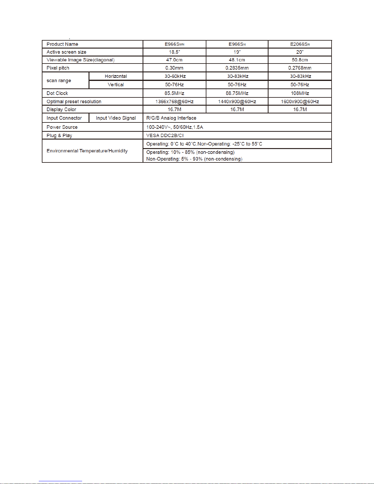
1. Monitor Specifications
Page 5
5
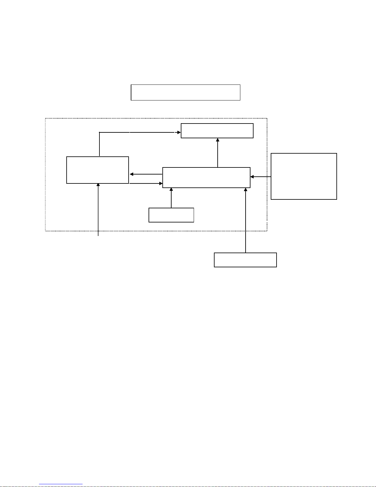
2. LCD Monitor Description
The LCD monitor will contain a main board, a power board, a key board which house the flat panel control logic,
brightness control logic and DDC.
The power part will provide AC to DC Inverter voltage to drive the backlight of panel and the main board chips each
voltage.
AC-IN
100V-240V
Monitor Block Diagram
Flat Panel and backlight
Main Board
RS232 Connector
For white balance
adjustment in factory
mode
Video signal, DDC
Key Board
Host Computer
Power Board
LED Drive.
Page 6
6
3. Operating Instructions
3.1 General Instructions
This monitor only has one external control function button; press the Power/Auto Configuration button to turn the
monitor on or off.
If you need to adjust other functions, please visit the official AOC website (www.aoc.com)to download and install
AOC’s exclusive i-Menu application software, and then perform related function adjustments to get the screen you
require.
• Connect the power cord properly.
• Connect the signal cable onto the PC’s graphics card.
• Push the button to start the monitor, and the power indicator will light up..
3.2 Control Buttons
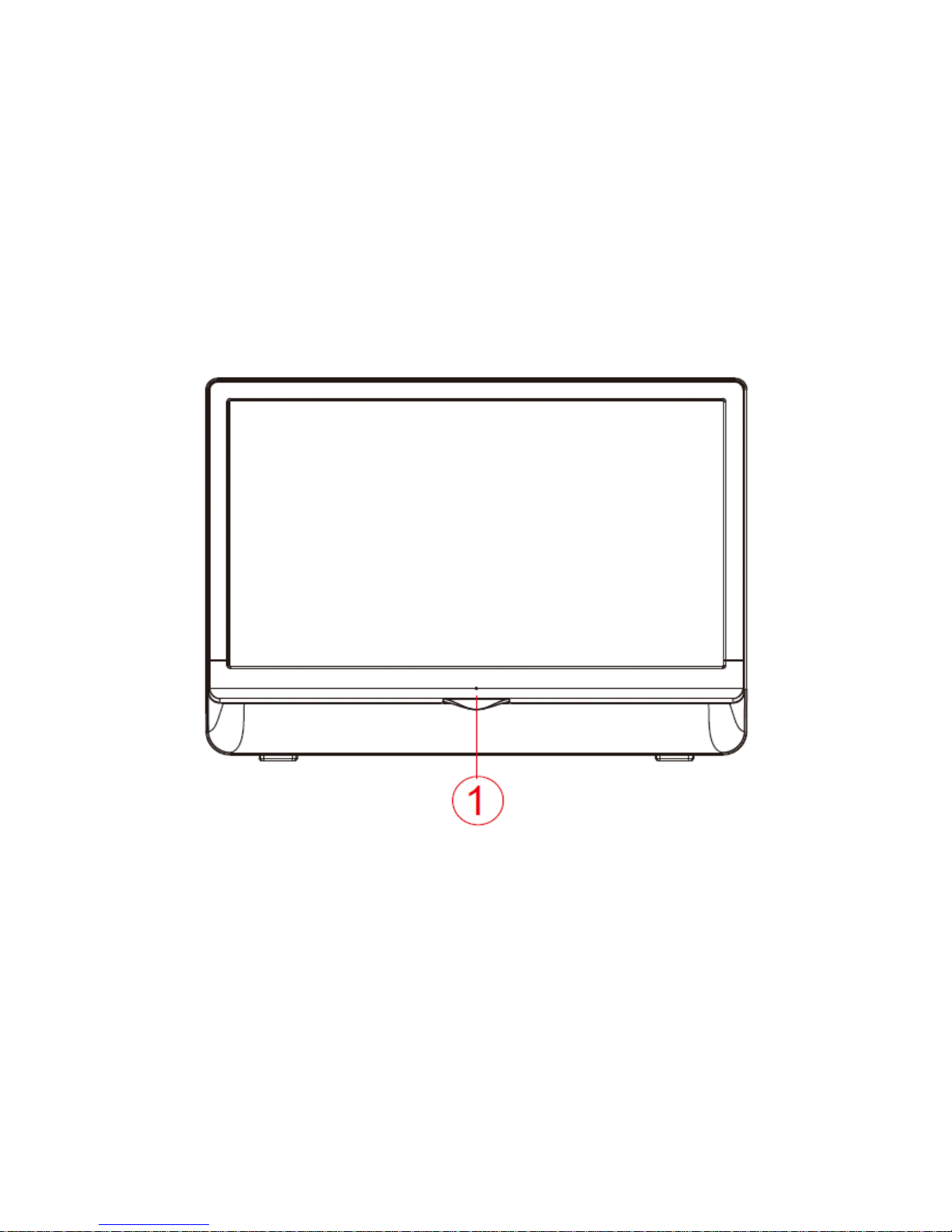
1.Power/ Auto Configuration
• Power/ Auto Configuration:
• When Power on, press Power/ Auto Configuration button to do auto configure .
• When Power off, press Power/ Auto Configuration button to turn on the monitor .
• When Power on, press Power/ Auto Configuration button continuously about 2 seconds to turn off the monitor .
• LED Indicator: Green—Full Power Mode. Flickering Green—Active-off Mode.
Page 7
7
NOTE:
Power/ Auto Configuration
• Do not place the monitor close to heat sources such as heaters, ventilation ducts or places exposed to direct
sunlight.Do not place it at dusty places or places that make the machine shake or impact either.
• Keep the original package box and packing materials; if you need to transport your monitor again, they will
come in handy.
• For maximum protection, please pack the monitor the way it was packed when shipped out of the factory.
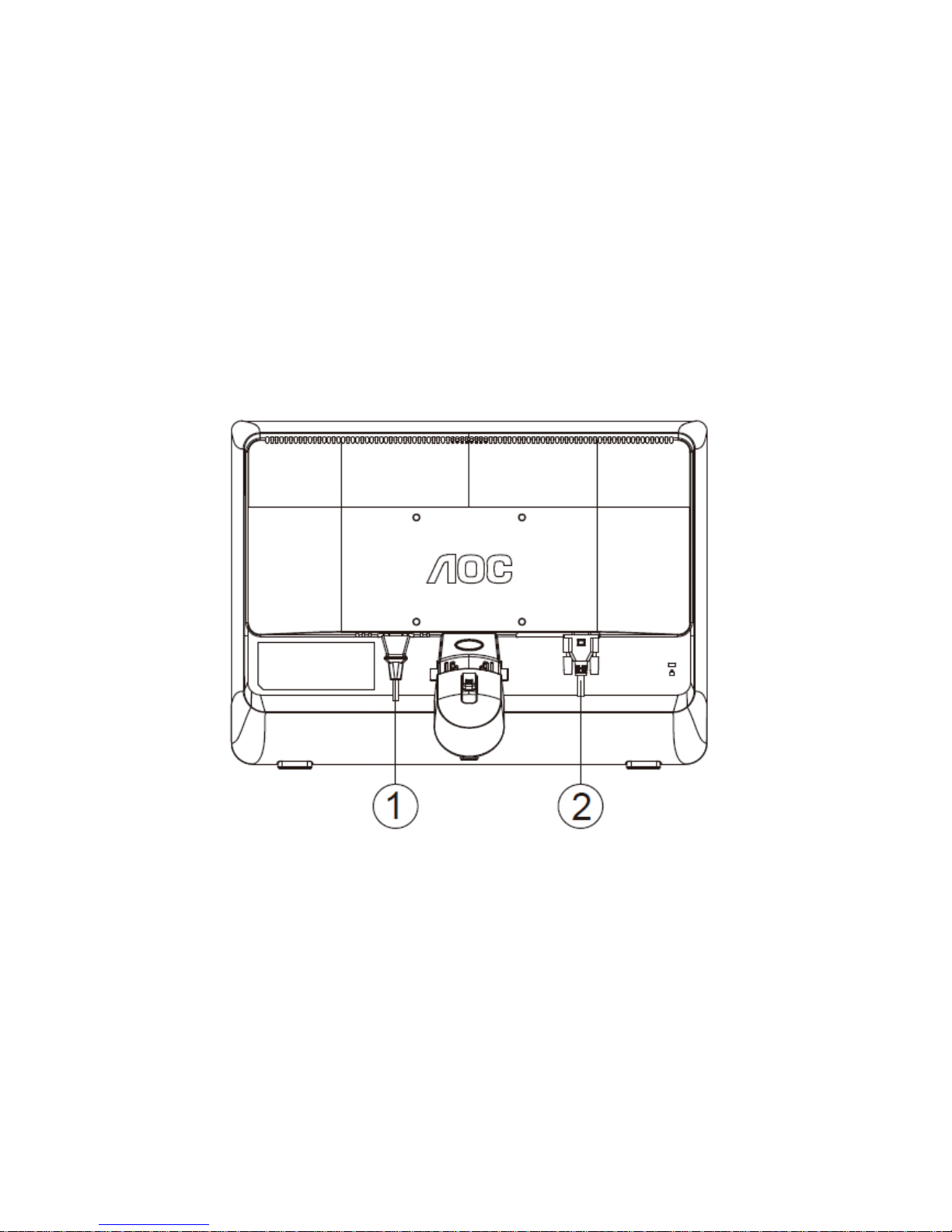
1.Power
2.Analog (DB-15 VGA cable)
To protect equipment, always turn off the PC and LCD monitor before connecting.
1 Connect the power cable to the AC port on the back of the monitor.
2 Connect one end of the 15-pin D-Sub cable to the back of the monitor and connect the other end to the computer’s
D-Sub port.
3 Turn on your monitor and computer
.
Page 8
8
4. Input/Output Specification
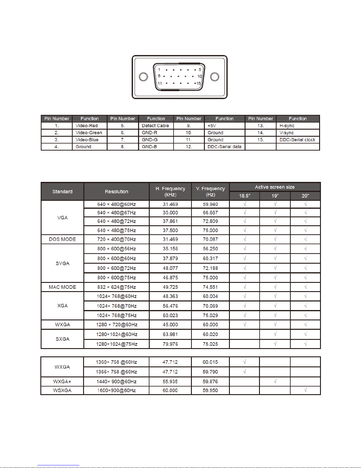
4.1 Input Signal Connector
Pin Assignments
15-Pin Side of the Signal Cable
4.2 Factory Preset Display Modes
Page 9
9
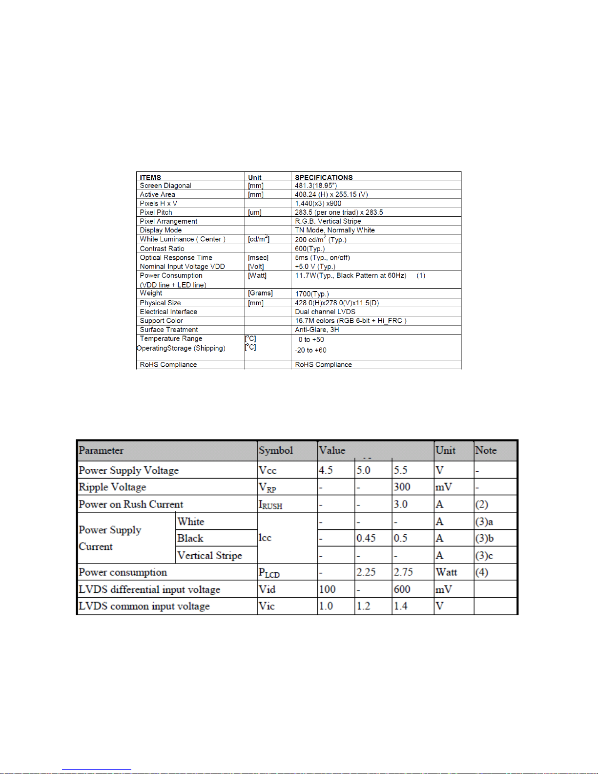
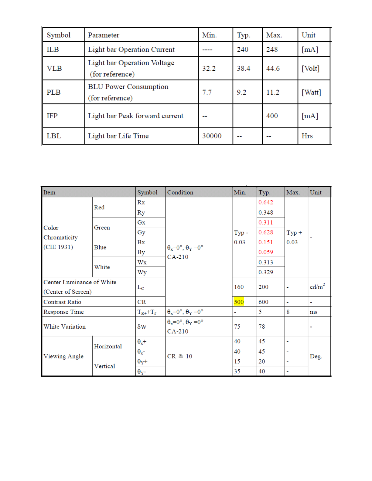
4.3 Panel Specification
4.3.1 General Features
This specification applies to the 18.95 inch Color a-Si TFT-LCD Module TPM190A1-MWW4. The display supports
the1440(H) x 900(V) screen format and 16.7M colors (RGB 6-bits + Hi-FRC data). The light source of this TFT-LCD
module is W-LED. All input signals are 2-channel LVDS interface and this module doesn’t contain a driver for
backlight.
4.3.2 Display Characteristics
4.3.3 Electrical Characteristics
TFT LCD MODULE
Vcc = 5.0 V, Ta = 25 ± 2 ºC, fv = 60 Hz
LED Characteristics
Page 10
10
4.3.4 Optical Characteristics
VDD = 5.0V, Frame rate = 60Hz, Clock = 78MHz, IBL = 7.5mA, Ta =25±2 ℃
Page 11
11
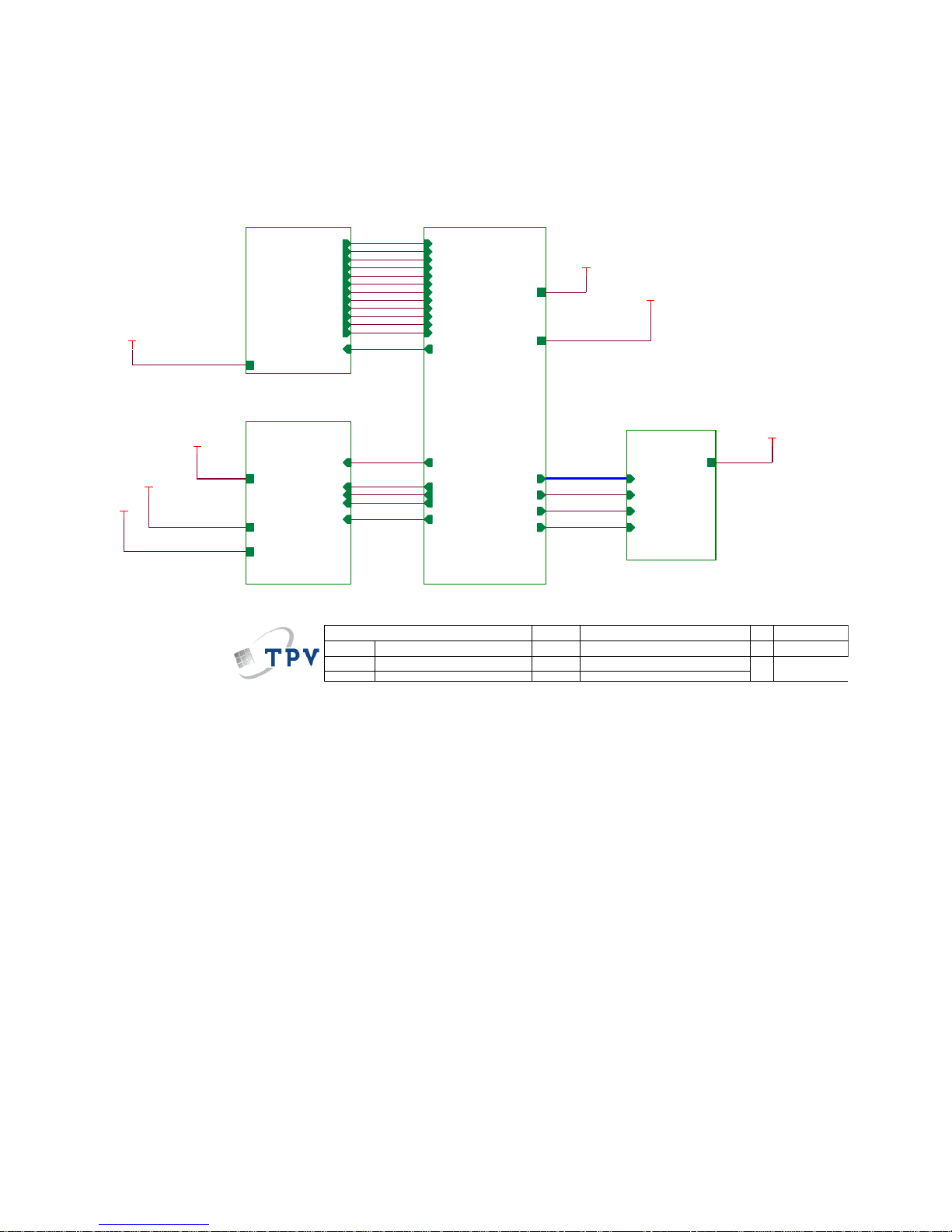
5. Block Diagram
5.1 Main Board
04.Output
04.Output
PPWR_ON#
L/T_SCL
L/T_SDA
CMVCC
PB[0..9]
CMVCC1
RTD2270CLW-CG SCHEMATIC
CMVCC1
LVDS OUTPUTXGA/SXGA
OEM MODEL Size
Rev
Date
Sheet of
TPV MODEL
PCB NAME
称爹
T P V ( Top Victory Electronics Co . , Ltd. )
Key Component
絬 隔 瓜 絪 腹
AOC 66S ID(1A) - 18.5" only A
AOC 66S ID(1A) - 18.5" only
A
3 7Wednesday , January 11, 2012
715G4488-M0A-001-0040
<称爹>
01.Top
715G4488-M0A-001-0040_120106
02.Input
DSUB_R+
DSUB_G+
DSUB_B+
DSUB_V
DSUB_RDSUB_G-
DSUB_B-
DET_CABLE
DSUB_H
DSUB_SOG
DDC1_SDA
DDC1_SCL
CMVCC1
EDID_CTRL
05.Power
on_BACKLIGHT
Adj_BACKLIGHT
CMVCC
VCC3.3
Mute
Volume#
PANEL_ID#
CMVCC1
03.Scalar
DSUB_R+
DSUB_G+
DSUB_SOG
DSUB_B+
DSUB_RDSUB_G-
DSUB_BDSUB_H
DSUB_V
Adj_BACKLIGHT
VCC3.3
PB[0..9]
DDC1_SDA
DDC1_SCL
DET_CABLE
on_BACKLIGHT
PPWR_ON#
PANEL_ID#
Volume#
Mute
CMVCC1
EDID_CTRL
L/T_SCL
L/T_SDA
VCC3.3
CMVCC
CMVCC
VCC3.3
PB[0..9]
CMVCC1
Page 12
12
5.2 Power Board
5V
EMI filter
Start Resistor
(R919,R920,R921,R922)
PWM Control
(IC901)
Transformer
AC input
15V
Bridge
Rectifier
and Filter
Feedback
Circuit
Rectifier
diodes
Photo coupler
(IC902)
D801
15V
MOSFET
(Q801)
ON/OFF
DIM
L801
LED
(CN804)
PWM Control
OZ9998BGN
(U801)
Regulator
(IC903)
Page 13

13
6. Schematic
6.1 Main Board
715G4488M02000004C
VGA_PLUG
EDID_CTRL
C104
5PF 50V
C108
5PF 50V
C111
5PF 50V
CMVCC1 5
R109
1K 1/16W 5%
DDC1_SCL5
C435
1N50V
D403
LBAV70LT1G
U103
AZC398-04S
I/O1
1
GND
2
I/O23I/O3
4
NC
5
I/O4
6
U102
AZC398-04S
I/O1
1
GND
2
I/O23I/O3
4
NC
5
I/O4
6
DSUB_SCL
056G 662504 эΘ2nd source
DSUB_SDA
R472
4K7 1/16W 5%
R473
4K7 1/16W 5%
VGA_R+ VGA_B+
VGA_G+
V_Sync
FB103
19R 0.5A
1 2
C107
47nF 16V
C103
22PF 50V
R111
100R 1/16W 5%
R104
100R 1/16W 5%
FB102
19R 0.5A
1 2
C105
47nF 16V
FB101
19R 0.5A
1 2
R101 0R05 1/10W R102 100R 1/16W 5%
R117
100R 1/16W 5%
C113
47nF 16V
C110
47nF 16V
C102
22PF 50V
R106
2K2 1/16W 5%
R112
75 OHM +-5% 1/16W
R107
75 OHM +-5% 1/16W
C109
47nF 16V
R105
2K2 1/16W 5%
R115
100R 1/16W 5%
R108
100R 1/16W 5%
R103 100R 1/16W 5%
C101
47nF 16V
R116
75 OHM +-5% 1/16W
R114
100R 1/16W 5%
GND POWER
R118
100K 1/16W 5%
DSUB_5V
DGND
H_Sync
DSUB_SDA
DDC1_SDA5
DSUB_H 5
DSUB_V 5
DET_CABLE 5
DSUB_R- 5
DSUB_R+ 5
DSUB_G- 5
ミ
ΑCONN
DSUB_G+ 5
DSUB_SOG 5
DSUB_B- 5
DSUB_B+ 5
U405
AT24C02C-SSHM-T
A0
1
A1
2
A2
3
GND4SDA
5
SCL
6
WP
7
VCC
8
DDC1_SCL
DSUB_SCL
VGA_PLUG
DDC1_SDA
OEM MODEL Size
Rev
Date
Sheet of
TPV MODEL
PCB NAME
称爹
T P V ( Top Vict ory Electronic s Co . , Ltd. )
Key Component
絬 隔 瓜 絪 腹
AOC 66S ID (1A) - 18.5" only A
AOC 66S ID (1A) - 18.5" only
B
4 7Wednesday , January 11, 2012
715G4488-M0A-001-0040
<称爹>
02.Input
715G4488-M0A-001-0040_120106
R474
22K 1/16W 5%
CN101
DB15
1
7
2
8
3
9
4
10
5
11
12
13
14
15
17 16
6
C434
220N16V
CMVCC1
R475 47R 1/16W 5%
V_Sync
DSUB_5V
VGA_R-
R476 47R 1/16W 5%
VGA_R+
VGA_G-
VGA_B+
DSUB_5V
CMVCC1
DSUB_SCL VGA_PLUG
VGA_G-
C106
22NF25V
VGA_G+DSUB_SDA
VGA_R-
ZD103
RLZ5.6B
1 2
VGA_B-
VGA_B-
VGA_G+
VGA_B+H_Sync
VGA_R+
Page 14

14
CMVCC1
ZD402
NC/MLVS0603M04
1 2
ZD404
NC/MLVS0603M04
1 2
ZD403
NC/MLVS0603M04
1 2
DSUB_V3
POWER_KEY#
DSUB_H3
DSUB_B-3
DSUB_B+3
DSUB_SOG3
DSUB_G-3
DSUB_G+3
DSUB_R-3
DSUB_R+3
KEY1
R489 22R 1/16W 5%
R490 22R 1/16W 5%
R492 22R 1/16W 5%
R491 22R 1/16W 5% R452 NC
R426 NC
PB[0..9] 5
MSDA
R451 NC
MSCL
LED_GRN/BLUE
on_BACKLIGHT 7
adj_BACKLIGHT 7
Volume# 7
Mute 7
PPWR_ON# 6
DET_CABLE 4
POWER_KEY#
VCC3.37
PANEL_ID# 7
CMVCC1
R469
NC/2K2 1/16W 5%
LED_O
LED_G/B
R493 NC
LED_ORANGE/TOUCH _VCC
LED_GRN/BLUE
R494 NC
R461 NC/0R05 1/16W
CMVCC17
VCC3.3
DDC1_SDA3
KEY2
Q402
NC/LMBT3906LT1G
Q403
LMBT3906LT1G
VCC3.3
VCC3.3
KEY1
R453 NC
MSCL
R424 NC
EE_WP
R468 330OH M 1/10W
C429
NC
EE_WP
MSDA
R481
NC/0R05 1/16W
R455
NC
R454
NC
U403
NC/M24C04-WMN6TP
NC
1
E1
2
E2
3
VSS4SDA
5
SCL
6
WC
7
VCC
8
PB1
PB[0..9]
PB0
PB4
PB2
PB5
PB3
R421
3K9 +/-5% 1/16W
KEY2
X401
14.31818MHZ/32PF
1 2
PB9
PB6
PB8
CN408
CONN
1
2
3
4
5
6
PB7
CN409
NC/CONN
1
2
3
4
5
6
7
LED_O
When use touch
Key,GPIO_P07 as
to control touch
key VCC
LVDS
LED_G/B
VCC3.3
FB405
NC
C436 100N 16V
VCC3.3
VCC1.2
R407
NC/10K 1/16W 5%
R404
NC/10K 1/16W 5%
CN406
NC/CONN
1
2
3
4
5
6
7
8
If product spec is <0.3W, need to
check flash VCC current.
R462 NC/0R05 1/16W
OEM MODEL Size
Rev
Date
Sheet of
TPV MODEL
PCB NAME
称爹
T P V ( Top Victory Elect ronics Co . , Ltd. )
Key Component
絬 隔 瓜 絪 腹
AOC 66S ID(1A) - 18.5" only
A
AOC 66S ID(1A) - 18.5" only
C
5 7Thursday, F ebruary 23, 2012
715G4488-M0A-001-0040
<称爹>
03.Scalar
715G4488-M0A-001-0040_120106
R463 NC
R464 NC
+
C423
100UF 16V
EDID_CTRL
R485 100R 1/16W 5%
(0)
LBADC1
(2K)
(2K) 1.118V
MENU
LBADC2
0.673V
UP
1.118V
(1K)
CN402
NC/CONN
1
2
3
4
5
6
0V
DOWN
AUTO
(KEY2)
(KEY1)
VCC3.3
CN407
NC/CONN
1
2
3
4
5
6
7
R405 100R 1/16W 5%
R427
NC/3K9 +/-5% 1/ 16W
C407
100N16V
C412 20pF
FB404
NC
L/T_SCL
4
L/T_SDA 4
C411 20pF
R466
2K2 1/16W 5%
R428
NC/3K9 +/-5% 1/ 16W
R411 NC/1K 1/16W 5%
R419 NC/100R 1/ 16W 5%
C404
1UF 10V
LED_ORANGE/TOUCH _VCC
C408
220N16V
C403
100N16V
C433
NC
C413NC/100N16V
R410 NC/10K 1/16W 5%
TOUCH_POWER
R414 10K 1/16W 5%
C417
NC/100N16V
C414NC/100N16V
R487
10K 1/16W 5%
R420 1K 1/16W 5%
C416
NC/100N16V
U402
MX25L2026DM1I-12G
CS
1
SO
2
WP
3
GND4SI
5
SCK
6
HOLD
7
VCC
8R408
10K 1/16W 5%
RTD2270CLW-CG
U401
R+
13
G+
10
SOG0
11
B+
8
R-
12
G-
9
B-
7
HSYNC0
16
VSYNC0
17
REXT
4
NC
15
ADC_GND
14
SPI_SDO
21
SPI_SCL
23
SPI_CE
22
SPI_SDI
24
P5.1/PWM1
27
GPIO/PWM3/CLKO1
56
XIN
1
XOUT
2
TXE2+
35
TXE2-
36
TXE1+
37
TXE1-
38
TXE0+
39
TXE0-
40
TXO3+
41
TXO3-
42
TXOC+
43
TXOC-
44
TXO2+
45
TXO2-
46
TXO1+
47
TXO1-
48
TXO0+
49
TXO0-
50
TXE3-
34
TXE3+
33
GND
5
ADC_VDD33
6
DGND
32
DGND
31
NC
52
DVDD12
30
DDCA_SDA/R S232_TX
18
DDCA_SCL/rs 232_RX
19
GPIO/PWM5
62
P5.0//PWM0
20
P5.2/PWM2
28
GPIO/INT1
55
GPIO/ADC1
58
GPIO/ADC2/I 2C_MDL_2A
59
GPIO/ADC3/I 2C_MDA_2A
60
GPIO/PWM4
61
GPIO/INT0/TCON7/ I2C_MDA_2B
63
GPIO/T2EX
64
P3.6/I2C_MDA
25
P3.7/I2C_MCL
26
RST
54
PVDD33
51
DVDD12
53
P1.0/T2
29
GPIO/ADC0
57
GND
3
C415NC/100N16V
+
C410
NC/10UF 50V R418 NC/100R 1/ 16W 5%
C401
100N16V
C406
100N16V
R401
0R05 1/16W
R402
560R 1/16W 5%
R412 NC/1K 1/16W 5%
R417
NC/10K 1/16W 5%
R403 390R 1/16W 1%
Near to Connect
R413 100R 1/16W 5%
FB401
30OHM
CMVCC1
VCC3.3
VCC3.3
VCC1.2
AVDD
AVDD
AVDD
VCC3.3
ZD401
NC/RLZ5. 6B
LED_ORANGE/TOUCH _VCC
TOUCH_POWER
R471 N C/470OHM +-5% 1/10W
DDC1_SCL3
Page 15

15
PB[0..9]5
PPWR_ON#5
PB0
CMVCC 7
PPWR_ON#
L/T_SDA
L/T_SCL
Q404
LMBT3906LT1G
+
C421
100UF 16V
FB402
120R 6A
R436
100K 1/16W 5%
Q405
AO3401A
C420
100N16V
C419
100N16VR433
10K 1/16W 5%
PANEL_VCC
PANEL_VCC
CMVCC
L/T_SCL 3
L/T_SDA 3
Q411
NC/AO4411
S1S2S
3G4
D8D7D6D
5
R434
300 OHM 1/4W
OEM MODEL Size
Rev
Date
Sheet of
TPV MODEL
PCB NAME
称爹
T P V ( Top Victory Electronics Co . , Ltd. )
Key Component
絬 隔 瓜 絪 腹 AOC 66S ID(1A) - 18.5" only A
AOC 66S ID(1A) - 18.5" only
A
6 7Tuesday, January 17, 2012
715G4488-M0A-001-0040
<称爹>
04.Output
715G4488-M0A-001-0040_120106
PB9
PB8
PB7
PB6
PB5
PB4
PB3
PB4
PB[0..9]
PB3
PB1
PB0
PB2
PB5
PB8
PB9
PB7
PB6
PB2
PB1
R488
NC/82 KOHM +-5% 1/16W
R435
10K 1/16W 5%
R488 reserved for fixing inrush current issue
2
D
S
1
G
AO3401A
3
CN403
CONN
1
2
3
4
5
6
7
8
9
10
11
12
13
14
15
16
17
18
19
20
21
22
23
24
25
26
27
28
29
30
Page 16

16
VCC3.3 4, 5
R441
4K7 1/16W 5%
Mute 5
adj_BACKLIGHT 5
on_BACKLIGHT 5CMVCC1 5
CMVCC5
R442
100R 1/16W 5%
+
C426
100UF 16V
+
C427
100UF 16V
R439
10K 1/16W 5%
C425
NC
C422
100N16V
R449
NC
C428
100N16V
CMVCC
VCC3.3
VCC3.3VCC3.3
CMVCC1
CMVCC1
CMVCC1
U406
AP1117E33L-13-77
ADJ(GND )
1
VOUT
2
VIN
3
4
4
CN404
CONN
1
2
3
4
5
6
7
8
9
R450 NC/10K 1/ 16W 5%
R437
10K 1/16W 5%
BKLT-EN
BKLT-VBRI
Volume
BKLT-EN
CMVCC
BKLT-VBRI
CMVCC
U404
NC/G1117-33T43UF
ADJ(GND )
1
VOUT(TAB)
2
VIN
3
Volume# 5
OEM MODEL Size
Rev
Date
Sheet of
TPV MODEL
PCB NAME
称爹
T P V ( Top Victory Electronics Co . , Ltd. )
Key Component
絬 隔 瓜 絪 腹 AOC 66S I D(1A) - 18.5" only A
AOC 66S I D(1A) - 18.5" only
B
7 7Thursday, January 12, 2012
715G4488-M0A-001-0040
<称爹>
05.Power
715G4488-M0A-001-0040_120106
Mute
Q406
LMBT3904LT1G
PANEL_ID# 5
U404 can use package 223 or 252.
R440
22K 1/16W 5%
Page 17

17
6.2 Power Board
715G4452P02002001M
R911
1.5K 1/10W
R919
100K
C919
2.2NF
R910
560 OHM 1/4W
D901
FR107
093G 6 026T5 2T
!
!
C902 680PF 250V
R901
1 MOHM +-5% 1/4W
R902
1 MOHM +-5% 1/4W
MNT 禯瞒2.5mm / TV 禯瞒3mm
BRIDGE 玡 L/N Trace 3.0mm
+5V
ZD901
MTZJ T-72 18B
1 2
Q903
KTD1028
+5V
R918
250R
FB901
BEAD
1 2
F902
T5AL 250V
D904 SR504-30
1 2
+
C914
470uF 16V
R912
12K 1/10W 1%
+
C909
1000UF 10V
R904 100 OHM 1/4W
R900
1 MOHM +-5% 1/4W
R917
1K 1/10W 1%
L905
1.1uH
CN901
SOCKET
12
3
R916
470OHM +-5% 1/10W
2A
2A
2A
C916
10N 50V
D903 SR510-22
1 2
100V-1
IC902
EL817M(X)
1
23
4
IC903
TL431G-A-TA
400V-1
+15VC900
1NF 250V
600V-1
R921
100K
R920
100K
R922
100K
200V-2
C911
2.2NF
C910
2.2NF
t
NR901
NTCR
12
+
C908
47uF/50V
C917
100N 50V
GND3
GND
1
2
C904
0.22UF275V
F901
2A
D906 SR504-30
1 2
200V-1
D902
FR107
R905 100 OHM 1/4W
R906 100 OHM 1/4W
R907 47 OHM 1/4W
R908 47 OHM 1/4W
R909 47 OHM 1/4W
+15V
GND2
GND
1
2
GND1
GND
1
2
1A
R903
0.39R
+
C913
NC/680uF 10V
R926
1.5 OHM 1/4W
T901
POWER X'FMR
1
2
3
4
5
6
7
8
9
10
D908 NC
1 2
!
+
C912
680uF 25V
L901
30mH
142
3
!
C901
100N 50V
!
C921
4.7nF
R923
12K 1/8W
C906
1500PF2KV
L903
3.5uH
+
C907
68uF 450V
R927
6.2K OHM +-1% 1/8W
C905
3.3NF 50V
DIM
IC901
LD7904JGP7
NC
1
COMP
2
GND
3
S4DRAIN
5
VCC
6
D905 SR510-22
1 2
ON/OFF
CN902
Wire Harness
1
2
3
4
5
6
7
8
9
OEM MODEL Size
Rev
Date
Sheet of
TPV MODEL
PCB NAME
称爹
T P V ( Top Vict ory Electronics C o . , Ltd. )
Key Component
絬 隔 瓜 絪 腹
PLPCC9341MHD1 1
Custom
Friday, June 08, 2012
715G4452-P02-002-0010
ODM MODEL
02.POWER
G4452-P02-002-0010-1-120528
AOC 66TH
2
3
C920
2.2NF
HS1
HEAT SINK(IC 901)
1
2
L901A
NC
124
3
R928
NC
C903 680PF 250V
!
R914
NC
!
R913
30KOHM +-1% 1/8W
R915
30KOHM +-1% 1/8W
-
+
BD901
2KBP08M-70
2
1
3
4
C915
100N 50V
HV
Page 18

18
+
C801
330UF25V
R815
1M 1% 1/8W
C810
NC
C814
100N 50V
L801
47UH
R802
300K 1/8W
+15V
CN804
NC12
3
4
5
6
7 8
ISW 0.1~0.3V
R807
10 OHM 1/8W
R806
100 OHM 1%
C817
NC
100V-2
R809
200K 1/8W 1%
R801
10K 1/4W
2A
2A 1.5A
D801
NC
1 2
R816
47K 1/8W 1%
C803
1N 50V
FB802
JUMP
1 2
U801
OZ9998BGN
ISEN1
13
ISEN2
14
GND
15
ISEN316ISEN4
1
ISET
2
OVP
3
RT
4
ENA
5
ISW
6
LDR
7
VREF8VIN
9
STATUS
10
SSTCMP
11
PWM
12
FB801
BEAD
1 2
Q801
APM1105NUC-TRG
C805
2.2UF 16V
+
C809A
4.7uF100V
C815
1N 50V
C804
0.47UF 50V
R823
NC
C811
NC
C816
1000PF500V
CN803
CONN
1
2
R804
10 OHM 1/8W
R824
0R05 1/10W
C812
100PF 50V
R825
0R05 1/10W
C808
NC
R826
0R05 1/10W
R805
100K 1/8W
D801A
SR3100-MK18
1 2
C807
0.47UF 50V
ON/OFF
DIM
FB804
BEAD
1 2
OEM MODEL Size
Rev
Date
Sheet of
TPV MODEL
PCB NAME
称爹
T P V ( Top Victory Electronics Co . , Ltd. )
Key Component
絬 隔 瓜 絪 腹 PLPCC9341MHD1 1
Custom
Friday, June 08, 2012
715G4452-P02-002-0010
ODM MODEL
03.CONVERTER
G4452-P02-002-0010-1-120528
AOC 66TH
3
3
C802
10N 50V
CN805
NC/CON N
1
2
3
4
5
R820
1 OHM +-5% 1/8W
R821
1 OHM +-5% 1/8W
FB803
BEAD
1 2
R814
NC
R827
0R05 1/4W 5%
R812
0.3R 1/4W
+
C809
NC
R822
1 OHM +-5% 1/8W
R819
1 OHM +-5% 1/8W
C806
220N 50V
R810
10K 1/8W 1%
R811
10K 1/8W 1%
R803
300K 1/8W
R818 10K 1/4W
R813
0.3R 1/4W
R817
680R
C813
680P 50V
Page 19

19
6.3 Key Board
715G5578K01000001S
LED_1#
SW001
SW
POWER
OEM MODEL Size
Rev
Date
Sheet of
TPV MODEL
PCB NAME
称爹
T P V ( Top Vict ory Electronic s Co . , Ltd. )
Key Component
絬 隔 瓜 絪 腹
AOC E966SWN B
AOC E966SWN
B
2 2Thursday, February 09, 2012
715GXXXX-K0A
<称爹>
2.0.key
RDGXXXX-K0A-000-0040
LED001
LED
1 2
ZD001
NC/MLVS0603M04
1 2
ZD002
NC/MLVS0603M04
1 2
R001 100R 1/ 10W 5%
SGND
SGND
CN001
Wire Harness
1
2
3
Page 20

20
7. PCB Layout
7.1 Main Board
715G4488M02000004C
Page 21

21
7.2 Power Board
715G4452P02002001M
Page 22

22
Page 23

23
7.3 Key Board
715G5578K01000001S
Page 24

24
8. Maintainability
8.1 Equipments and Tools Requirement
1. Voltmeter.
2. Oscilloscope.
3. Pattern Generator.
4. DDC Tool with an IBM Compatible Computer.
5. Alignment Tool.
6. LCD Color Analyzer.
7. Service Manual.
8. User Manual.
Page 25

25
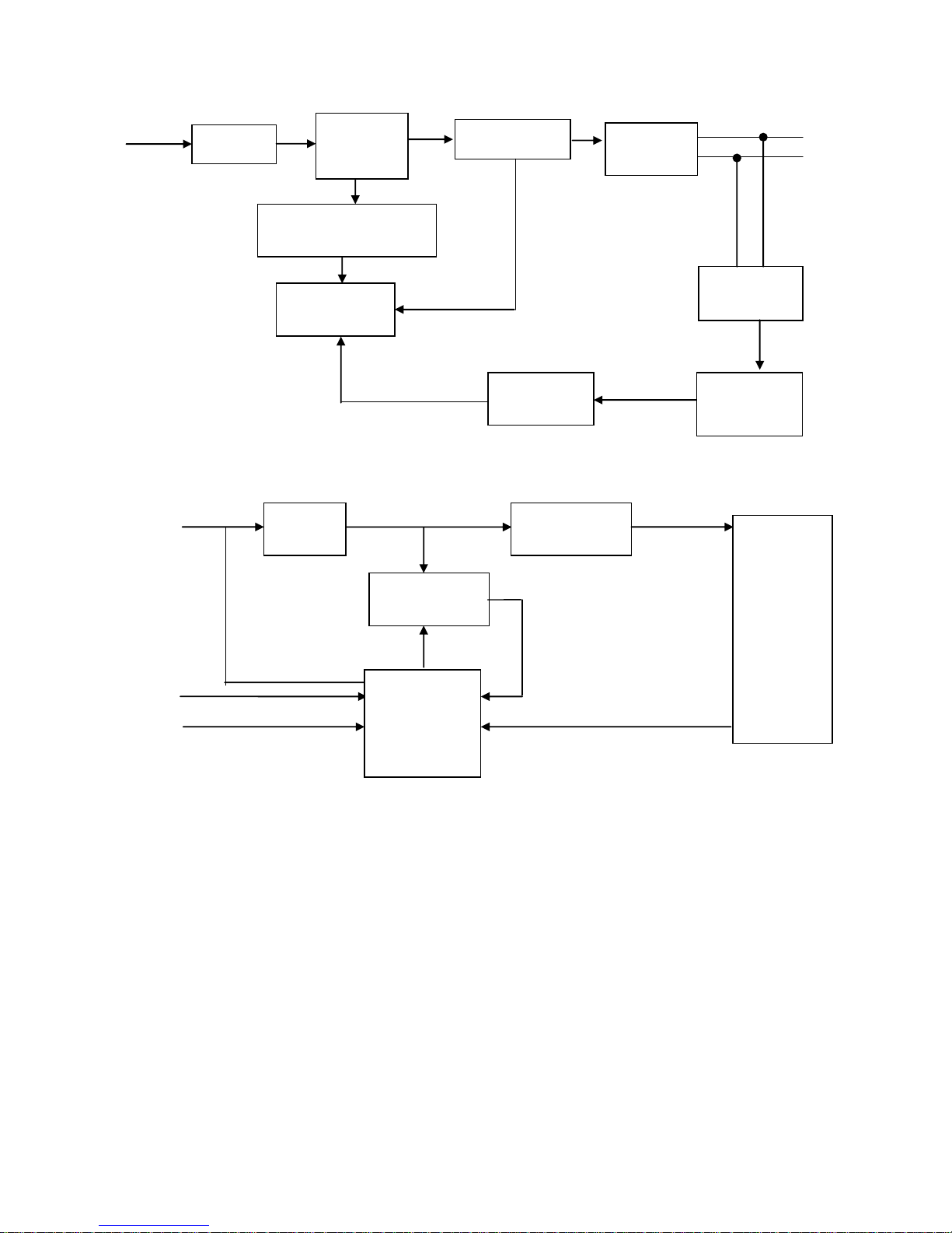
8.2 Trouble Shooting
1. No Power
OK
NG
No power
Check power cable is
tightened?
Check Power “On/Off”
is “On”?
Re-plug the power cable
Replace main board and check connections
Check the LED
indicate is OK?
Check the AC power
Replace the converter board
OK
NG
OK
NG
Turn on the Power “On/Off” switch
Replace key board and check connections
Page 26

26
2. No Video (Power LED Blue)
No Video (Power LED Blue)
Press the power
button is OK?
Check the LVDS/FFC
cable or panel
The end
NG
OK
Replace the main board
Replace the converter
board
Replace the LVDS/FFC
cable or panel
The end
Replace the key board
OK
Replace the main
board and connection
OK
Page 27

27
3. DIM
OK
The end
OK
The end
OK
The end
DIM (image overlap, focus or flicker)
Reset in factory mode
Set to the optimal
frequency, select the
recommended frequency
Pull out signal cable and
check “Self Test Feature
Check” is ok?
Check the signal cable
and the PC
Readjust the phase and pixel
clock in the user mode
Replace the main board
Replace the panel
NG
NG
NG
OK
NG
NG
OK
The end
OK
NG
Page 28

28
4. Color is not optimal
NG
Color is not optimal
Miss color
Color shift
Replace the signal cable
Pull out the signal cable
and check the screen
color display is normal?
The end
Replace the signal cable or PC
Reset the factory mode
In the user mode, set the” color
settings” until customer satisfy
Replace the main board
NG
OK
NG
OK
NG
Page 29

29
9. White- Balance, Luminance Adjustment
Approximately 30 minutes should be allowed for warm up before proceeding white balance adjustment.
How to setting MEM channel you can reference to chroma 7120 user guide or simpl use “SC” key and “NEXT” Key
to modify xyY value and use “ID” key to modify the TEXT description Following is the procedure to do white-balance
adjust .
2. Setting the color temp. you want
A. MEM.CHANNEL 3 Warm (6500K):
Warm color temp. parameter is x = 313 ±30, y = 329 ±30
B. MEM.CHANNEL 4 Normal (7300K):
Normal color temp. parameter is x = 301 ±30, y = 317 ±30
C. MEM.CHANNEL 9 Cool (9300K):
Cool color temp. parameter is x = 283 ±30, y = 297 ±30
D. MEM.CHANNEL 10 (sRGB color):
sRGB color temp. parameter is x = 313 ±30, y = 329 ±30
3. Enter into the factory mode
A.USE the tool ,,double-click the icon and choose”Enter
Factory” You will enter into the factory mode
B. Press the MENU button,Pull out the power cord, then plug the power cord. Then the factory OSD will be at the left
top of the panel.
4. Gain adjustment:
Move cursor to “-F-” and press MENU key
Page 30

30
A. Adjust Warm (6500K) color-temperature
1. Switch the chroma-7120 to RGB-Mode (with press “MODE” button)
2. Switch the MEM.channel to Channel 3 (with up or down arrow on chroma 7120)
3. The LCD-indicator on chroma 7120 will show x = 313 ±30, y = 329 ±30
4. Adjust the RED on factory window until chroma 7120 indicator reached the value R=100
5. Adjust the GREEN on factory window until chroma 7120 indicator reachedthe value G=100
6. Adjust the BLUE on factory window until chroma 7120 indicator reached the value B=100
7. Repeat above procedure (item 4, 5, 6) until chroma 7120 RGB value meet the tolerance =100±2
B. Adjust Normal (7300K) color-temperature
1. Switch the chroma-7120 to RGB-Mode (with press “MODE” button)
2. Switch the MEM.channel to Channel 4 (with up or down arrow on chroma 7120)
3. The LCD-indicator on chroma 7120 will show x = 301 ±30, y = 317 ±30
4. Adjust the RED on factory window until chroma 7120 indicator reached the value R=100
5. Adjust the GREEN on factory window until chroma 7120 indicator reachedthe value G=100
6. Adjust the BLUE on factory window until chroma 7120 indicator reached the value B=100
7. Repeat above procedure (item 4, 5, 6) until chroma 7120 RGB value meet the tolerance =100±2
C. Adjust Cool (9300K) color-temperature
1. Switch the Chroma-7120 to RGB-Mode (with press “MODE” button)
2. Switch the MEM. Channel to Channel 9 (with up or down arrow on chroma 7120)
3. The LCD-indicator on chroma 7120 will show x = 283 ±30, y = 297 ±30
4. Adjust the RED on factory window until chroma 7120 indicator reached the value R=100
5. Adjust the GREEN on factory window until chroma 7120 indicator reached the value G=100
6. Adjust the BLUE on factory window until chroma 7120 indicator reached the value B=100
7. Repeat above procedure (item 4, 5, 6) until chroma 7120 RGB value meet the tolerance =100±2
D. Adjust sRGB color-temperature
1. Switch the chroma-7120 to RGB-Mode (with press “MODE” button)
2. Switch the MEM.channel to Channel 10 (with up or down arrow on chroma 7120)
3. The LCD-indicator on chroma 7120 will show x = 313 ±30, y = 329 ±30
4. Adjust the RED on factory window until chroma 7120 indicator reached the value R=100
5. Adjust the GREEN on factory window until chroma 7120 indicator reachedthe value G=100
6. Adjust the BLUE on factory window until chroma 7120 indicator reached the value B=100
7. Repeat above procedure (item 4, 5, 6) until chroma 7120 RGB value meet the tolerance =100±2
E. Turn the Power-button off to quit from factory mode.
Page 31

31
10. Monitor Exploded View
Page 32

32
11. BOM List
Note: The parts information listed below are for reference only, and are subject to change without notice. Please go
to http://cs.tpv.com.cn/hello1.asp for the latest information.
T9C5R92DDBA3NNE
Location
Part No.
Description
Remark
052G 2191 A
PAPER TAPE
ECN403
095G179J30P584
FFC CABLE 30PIN 145MM P1.0MM
0D1G1030 6120
screw
0M1G1740 8120
SCREW FOR STD/MF 42-D020715/42-D000649()
E08902
389G0722HAADBD
D-SUB CABLE 1200
E08901
389G414A12N0HL
AC POWER CORD 1200 for China
E750
750GBV190W4116N000
LCD TPM190A1-MWW4 R1 WH TPV
E750
750GBV190W4126N000
LCD TPM190A1-MWW4 R12 WH TPV
2nd source
H15G0073401101
MAINFRAME
H40G 001624 1A
CARTON LABEL BARCODE 1
H40G 45762413B
P/N LABEL FOR BASE
H40G 58169017B
CEL-1 LABEL
H40G019N615A13
RATING LABEL E966S PRC/AP
H40G058361513D
LABEL WIN7 EPA EPEAT
H41G18M161502A
MANUAL 66th CH
H44G6601001EPE
CUSHION
H44G90911010DJ
CUSHION EPS E966SN
H44G90912010DJ
CUSHION
H44G909161501A00HX
ARTWORK CARTON
H45G 77 6
PE PACKING
H45G 87 18 23
EPE COVER
KEPCCHA4
KEY BOARD
PLPCC9501UHD1
ADAPTER BOARD
Q33G0541AED 1L0100
KEY_POWER
Q33G0542ABJ01L0100
KEY
Q34G7561ABJ 1B0130
STAND
Q34G7562AED01B0130
BASE
Q34G7565AEDA5B0101
BEZEL
Q34G7566AED01B0130
REAR_COVER
Q41G2009615 9D
WARRANTY CARD
Q45G 76 28 H A
PROTECT BAG
Q50G 4 10
TIE (Y1900221)
M05201
Q52G100204500A00JY
AL FOIL
M05202
Q52G100204500A00JY
AL FOIL
M05203
Q52G100204500A00JY
AL FOIL
Q52G1301024A0100YY
BIG CARTON TAPE FOR AOC 60MM
Page 33

33
Q52G6019 14
TAPE
756GHCCB0A60050001
MAIN BOARD-CBPCCT6A1H2
SMTCC-U402
100GARL9022W11
MCU ASSY-056G2233 11
CN408
033G3802 6B Y L
WAFER
CN404
033G3802 9B Y L
CONN 2.0 9P
CN403
033G801930F CH L
FFC CONN 1.0mm 30P R/A 34mm 6mm
CN101
088G 35315F CH
D-SUB CONN WITH SCREW 15P
X401
093G 22 53CEC
CRYSTAL S-F-14.31818M-32-3030-2085-30
H40G 45762429A
LABEL
LED001
081G 2 3 1P
LED GPG2603T/R006-35A GUANGPU
CN001
395G820H03TW01
HARNESS 3P(SANW)-6P 200
GND1
009G6005 1
GND TERMINAL
GND2
009G6005 1
GND TERMINAL
CN803
033G8021 2E L
INVERT CONN 3.5mm 2P
IC902
056G 139 9
IC EL817M(X) photocoupler DIP-4
IC901
056G 379205
AC/DC LD7904JGP7 DIP-6
NR901
061G 58100 X1
NTCR 10 20% 3.6W
C904
063G107K224 UM
X2 CAP 0.22uF K 275VAC
C907
067G 43Z68015L
EC 68uF M 450V RGT 18*31.5mm
L901
073G 174 65 H2
LINE FILTER 30mH MIN
L903
073G 253 91 L
CHOKE COIL 3.5UH 10% CC-015367HF,VOC,HF
L905
073G 253191 H
IND CHOKE 1.1uH DADON
L801
073G 253242 CP
CHOKE COIL 47UH 10% 2.5A L040462-6
T901
080GL19P 39 CP
X'FMR 950UH 10% 20UH EFD25 T020543-6
CN901
087G 501 32 DL
AC SOCKET DIP 3PIN+2PIN GROUND
BD901
093G 50460519
BRIDGE KBP206G X0 2A 800V KBP 80A
D904
093G 60519
DIODE SR560-MK23 5A/60V DO-27 SECOS
D903
093G 60924
DIODE SR510-22 DO-201AD
D905
093G 60924
DIODE SR510-22 DO-201AD
CN902
095G 825 9DM02
HARNESS 9P-9P(2008) 100mm
D801A
393G0060A0300S
SCHOTTKY SR3100-MK18 3A 100V DO-201AD
709G4452 HM001
COMSUMPTIVE ASSY
H40G 45762429A
LABEL
C423
067G 3051014PT
EC 100UF 20% 25V 6.3*11 CD263
C427
067G 3051014PT
EC 100UF 20% 25V 6.3*11 CD263
C426
067G 3051014PT
EC 100UF 20% 25V 6.3*11 CD263
C421
067G 3051014PT
EC 100UF 20% 25V 6.3*11 CD263
R001
061G0603101 JT
RST CHIP 100R 1/10W 5% TZAI YUAN
055G 23524
WELDING FLUX WITHOUT PB
Q51G 6 4509
GLUE_RTV
Page 34

34
Q55G 100625
TIN STICK_LOW ARGENTUM
U801
056G 700 11
LED DRIVER OZ9998BGN-A1-0-TR SOP-16
Q801
057G 763141
MOSFET APM1105NUC-TRG 16A 100V
TO-252-3
R825
061G0603000 JF
RST CHIPR MAX 0R05 1/10W FENGHUA
R826
061G0603000 JF
RST CHIPR MAX 0R05 1/10W FENGHUA
R824
061G0603000 JF
RST CHIPR MAX 0R05 1/10W FENGHUA
R925
061G0603100 JF
RST CHIPR 10 OHM 5% 1/10W FENGHUA
R917
061G06031001FT
RST CHIP 1K 1/10W 1%
R912
061G06031202FT
RST CHIP 12K 1/10W 1%
R911
061G0603152 JF
RST CHIPR 1.5KOHM +-5% 1/10W FENGHUA
R916
061G0603471 JT
RST CHIPR 470OHM +-5% 1/10W TZAI YUAN
R807
061G0805100 JF
RST CHIPR 10 OHM +-5% 1/8W FENGHUA
R804
061G0805100 JF
RST CHIPR 10 OHM +-5% 1/8W FENGHUA
R810
061G08051002FT
RST CHIP 10K 1/8W 1%
R811
061G08051002FT
RST CHIP 10K 1/8W 1%
R815
061G08051004FT
RST CHIP R 1 MOHM +-1% 1/8W
R806
061G0805101 JF
RST 0805 100R 5% 1/8W
R805
061G0805104 JY
RST CHIPR 100KOHM 1/8W YAGEO
R819
061G0805109 JF
RST CHIPR 1 OHM +- 5% 1/8W FENGHUA
R820
061G0805109 JF
RST CHIPR 1 OHM +- 5% 1/8W FENGHUA
R821
061G0805109 JF
RST CHIPR 1 OHM +- 5% 1/8W FENGHUA
R822
061G0805109 JF
RST CHIPR 1 OHM +- 5% 1/8W FENGHUA
R923
061G0805123 JF
RST CHIPR 12KOHM +-5% 1/8W FENGHUA
R809
061G08052003FT
RST CHIP 200K 1/8W 1%
R913
061G08053002FF
RST CHIPR 30KOHM +-1% 1/8W FENGHUA
R915
061G08053002FF
RST CHIPR 30KOHM +-1% 1/8W FENGHUA
R803
061G0805304 JF
RST CHIPR 300KOHM +-5% 1/8W FENGHUA
R802
061G0805304 JF
RST CHIPR 300KOHM +-5% 1/8W FENGHUA
R816
061G08053902FT
RST CHIP 39K 1/8W 1%
R927
061G0805622 JT
RST CHIPR 6K2 +-5% 1/8W TZAI YUAN
R906
061G1206101 JT
RST CHIPR 100 OHM +-5% 1/4W TZAI YUAN
R904
061G1206101 JT
RST CHIPR 100 OHM +-5% 1/4W TZAI YUAN
R905
061G1206101 JT
RST CHIPR 100 OHM +-5% 1/4W TZAI YUAN
R801
061G1206103 JF
RST CHIPR 10KOHM +-5% 1/4W FENGHUA
R818
061G1206103 JF
RST CHIPR 10KOHM +-5% 1/4W FENGHUA
R922
061G1206104 JT
RST CHIPR 100KOHM +-5% 1/4W TZAI YUAN
R919
061G1206104 JT
RST CHIPR 100KOHM +-5% 1/4W TZAI YUAN
R921
061G1206104 JT
RST CHIPR 100KOHM +-5% 1/4W TZAI YUAN
R920
061G1206104 JT
RST CHIPR 100KOHM +-5% 1/4W TZAI YUAN
Page 35

35
R901
061G1206105 JF
RST CHIPR 1 MOHM +-5% 1/4W FENGHUA
R900
061G1206105 JF
RST CHIPR 1 MOHM +-5% 1/4W FENGHUA
R902
061G1206105 JF
RST CHIPR 1 MOHM +-5% 1/4W FENGHUA
R926
061G1206159 JT
RST CHIP R 1.5ohm 1/4W +/-5%
R812
061G1206308 JT
RST 1206 0.3R 5% 1/4W
R813
061G1206308 JT
RST 1206 0.3R 5% 1/4W
R909
061G1206470 JT
RST CHIPR 47 OHM +-5% 1/4W TZAI YUAN
R907
061G1206470 JT
RST CHIPR 47 OHM +-5% 1/4W TZAI YUAN
R908
061G1206470 JT
RST CHIPR 47 OHM +-5% 1/4W TZAI YUAN
R910
061G1206561 JT
RST CHIPR 560 OHM +-5% 1/4W TZAI YUAN
R817
061G1206681 JF
RST 1206 680R 5% 1/4W FENGHUA
C916
065G060310332K Y
CAP CHIP 0603 10N 50V X7R +/-10%
C812
065G080510131J F
CAP CHIP 0805 100PF J 50V NPO
C803
065G080510232K Y
CAP CHIP 0805 1N 50V X7R +/-10%
C815
065G080510232K Y
CAP CHIP 0805 1N 50V X7R +/-10%
C802
065G080510332K Y
CAP CHIP 0805 10N 50V X7R +/-10%
C814
065G080510432K 3
CAP CHIP 0805 100N 50V X7R +/-10%
C915
065G080510432K Y
CAP CHIP 0805 100N 50V X7R +/-10%
C917
065G080510432K Y
CAP CHIP 0805 100N 50V X7R +/-10%
C901
065G080510432K Y
CAP CHIP 0805 100N 50V X7R +/-10%
C806
065G080522432K Y
CAP CHIP 0805 220N 50V X7R +/-10%
C805
065G080522512K 3
CAP CHIP 0805 2U2 16V X7R +/-10%
C905
065G080533232K A
CAP 0805 3.3NF 10% 50V X7R
C807
065G080547432K 3
CAP 0805 470NF 10% 50V X7R
C804
065G080547432K T
CAP CHIP 0805 0.47UF K 50V X7R
C813
065G080568131J Y
CAP CHIP 0805 680P 50V NP0 +/-5%
C911
065G120622272K Y
CER 1206 2N2 500V X7R 10%
C910
065G120622272K Y
CER 1206 2N2 500V X7R 10%
C919
065G120622272K Y
CER 1206 2N2 500V X7R 10%
C920
065G120622272K Y
CER 1206 2N2 500V X7R 10%
ZD902
093G 39S 38 T
PTZ 9.1B
709G4452 HS001
COMSUMPTIVE ASSY
SW001
077G603S AI HJ
TACT SWITCH AI 2PIN SEALED
E715
715G5578K01000001S
KEY PCB FR1 SS 41*14*1.6mm
FB802
095G 90 23
JUMP WIRE - -
709G4452 HA001
COMSUMPTIVE ASSY
E715
715G4452P02002001M
PWR PCB FR1 CTI>600 SS 152*122*1.6MM
J9003
095G 90 23
JUMP WIRE - -
J9004
095G 90 23
JUMP WIRE - -
C801
367G215X3314AT
EC 330UF 20% 25V - 10*12
Page 36

36
F902
084G 56 5 C
FUSE 5A 250V MST 5A 250V
J9014
095G 90 23
JUMP WIRE - -
J9022
095G 90 23
JUMP WIRE - -
J9002
095G 90 23
JUMP WIRE - -
Q903
057G 530503 T
2SD1207T
C908
367G215X4707AT
EC 47uF 20% 50V - 6.3*11mm
D902
093G 6026T52T
CTIFIER DIODE FR107
J9009
095G 90 23
JUMP WIRE - -
R827
095G 90 23
JUMP WIRE - -
ZD901
093G 39A0852T
GDZJ18B
C816
065G517K102 2T6921
CAP CER 1000PF K 500V Y5P
J9016
095G 90 23
JUMP WIRE - -
J9020
095G 90 23
JUMP WIRE - -
J9007
095G 90 23
JUMP WIRE - -
J9006
095G 90 23
JUMP WIRE - -
C921
065G500K4722HT
CAP CER 4.7NF 10% 50V X7R
J9019
095G 90 23
JUMP WIRE - -
D901
093G 6026T52T
CTIFIER DIODE FR107
J9021
095G 90 23
JUMP WIRE - -
R918
061G152M25152T SY
RST MOF 250R 5% 2W
C914
367G415X4713AT
EC 470uf 20% 16V ERS1CM471G13B50TM 10X13
IC903
056G 563355
Shunt Regu TL431G-A-TA TO-92 42V 150mA
J9012
095G 90 23
JUMP WIRE - -
C906
065G 2K152 2T6921
CAP CER 1500pF K 2KV Y5P
FB801
071G 55 29
FERRITE BEAD
C903
365G306K6812WR
CAP Y1 680PF 10% 250V Y5P
J9015
095G 90 23
JUMP WIRE - -
C809A
067G 4154799LT
EC 4.7UF 20% 100V 8*11.5
J9005
095G 90 23
JUMP WIRE - -
FB804
071G 55 29
FERRITE BEAD
R903
061G152M39852T SY
RST MOF 0.39R 5% 2W
J9011
095G 90 23
JUMP WIRE - -
006G 31500
EYELET
C912
367G215S6814AT
EC 680UF 20% 25V - 12.5*16
C900
065G306M10233R
CAP Y1 1NF 20% 250V Y5U
F901
084G 56 3 C
FUSE 3.15A 250V MST 3.15A 250V
J9008
095G 90 23
JUMP WIRE - -
J9013
095G 90 23
JUMP WIRE - -
C902
365G306K6812WR
CAP Y1 680PF 10% 250V Y5P
FB803
071G 55 29
FERRITE BEAD
Page 37

37
C909
367G415X1024AT
EC 1000UF 20% 25V 12.5X20
FB901
071G 55 29
FERRITE BEAD
J9001
095G 90 23
JUMP WIRE - -
U404
056G 563 52
LDO AP1117D33G-13
U102
056G 662 52
ESD PROTECT AZC398-04S.R7G SOT23-6
U103
056G 662 52
ESD PROTECT AZC398-04S.R7G SOT23-6
U405
056G1133 34 1
EEPROM M24C02-RMN6TP 2Kb SO-8
U402
056G2233 11
FLASH Pm25LD020C-SCE 2M SIOC-8
Q407
057G 417525
SMALLTRAN MMBT3904 200mA 40V SOT-23
Q406
057G 417525
SMALLTRAN MMBT3904 200mA 40V SOT-23
Q404
057G 417526
SMALLTRAN MMBT3906 -0.2A -40V SOT-23
Q403
057G 417526
SMALLTRAN MMBT3906 -0.2A -40V SOT-23
Q411
057G 763 3
AO4411 SO-8 BY AOS
R401
061G0402000 JT
RST CHIPR MAX0R05 1/16W TZAI YUAN
R405
061G0402101 JT
RST CHIP 100R 1/16W 5% TZAI YUAN
R115
061G0402101 JT
RST CHIP 100R 1/16W 5% TZAI YUAN
R111
061G0402101 JT
RST CHIP 100R 1/16W 5% TZAI YUAN
R442
061G0402101 JT
RST CHIP 100R 1/16W 5% TZAI YUAN
R420
061G0402101 JT
RST CHIP 100R 1/16W 5% TZAI YUAN
R104
061G0402101 JT
RST CHIP 100R 1/16W 5% TZAI YUAN
R102
061G0402101 JT
RST CHIP 100R 1/16W 5% TZAI YUAN
R485
061G0402101 JT
RST CHIP 100R 1/16W 5% TZAI YUAN
R108
061G0402101 JT
RST CHIP 100R 1/16W 5% TZAI YUAN
R103
061G0402101 JT
RST CHIP 100R 1/16W 5% TZAI YUAN
R117
061G0402101 JT
RST CHIP 100R 1/16W 5% TZAI YUAN
R413
061G0402101 JT
RST CHIP 100R 1/16W 5% TZAI YUAN
R114
061G0402101 JT
RST CHIP 100R 1/16W 5% TZAI YUAN
R109
061G0402102 JT
RST CHIP 1K 1/16W 5% TZAI YUAN
R408
061G0402103 JT
RST CHIP 10K 1/16W 5% TZAI YUAN
R487
061G0402103 JT
RST CHIP 10K 1/16W 5% TZAI YUAN
R437
061G0402103 JT
RST CHIP 10K 1/16W 5% TZAI YUAN
R414
061G0402103 JT
RST CHIP 10K 1/16W 5% TZAI YUAN
R439
061G0402103 JT
RST CHIP 10K 1/16W 5% TZAI YUAN
R433
061G0402103 JT
RST CHIP 10K 1/16W 5% TZAI YUAN
R435
061G0402103 JT
RST CHIP 10K 1/16W 5% TZAI YUAN
R118
061G0402104 JT
RST CHIP 100K 1/16W 5% TZAI YUAN
R436
061G0402104 JT
RST CHIP 100K 1/16W 5% TZAI YUAN
R466
061G0402222 JT
RST CHIP 2K2 1/16W 5% TZAI YUAN
R106
061G0402222 JT
RST CHIP 2K2 1/16W 5% TZAI YUAN
R105
061G0402222 JT
RST CHIP 2K2 1/16W 5% TZAI YUAN
Page 38

38
R474
061G0402223 JT
RST CHIP 22K 1/16W 5% TZAI YUAN
R440
061G0402223 JT
RST CHIP 22K 1/16W 5% TZAI YUAN
R403
061G04023900FT
RST CHIP 390R 1/16W 1%
R421
061G0402392 JT
RST CHIP R 3K9 +/-5% 1/16W TZAI YUAN
R475
061G0402470 JT
RST CHIP 47R 1/16W 5% TZAI YUAN
R476
061G0402470 JT
RST CHIP 47R 1/16W 5% TZAI YUAN
R472
061G0402472 JT
RST CHIP 4K7 1/16W 5% TZAI YUAN
R473
061G0402472 JT
RST CHIP 4K7 1/16W 5% TZAI YUAN
R441
061G0402472 JT
RST CHIP 4K7 1/16W 5% TZAI YUAN
R402
061G0402561 JT
RST 0402 560R 5% 1/16W
R112
061G0402750 JT
RST 0402 75R 5% 1/16W
R116
061G0402750 JT
RST 0402 75R 5% 1/16W
R107
061G0402750 JT
RST 0402 75R 5% 1/16W
R101
061G0603000 JT
RST CHIP MAX 0R05 1/10W TZAI YUAN
R468
061G0603331 JT
RST 0603 330R 5% 1/10W
R477
061G1206331 JT
RST CHIPR 330 OHM +-5% 1/4W TZAI YUAN
C407
065G040210412K A
CAP CHIP 0402 100nF K 16V X7R
C401
065G040210412K A
CAP CHIP 0402 100nF K 16V X7R
C413
065G040210412K A
CAP CHIP 0402 100nF K 16V X7R
C422
065G040210412K A
CAP CHIP 0402 100nF K 16V X7R
C428
065G040210412K A
CAP CHIP 0402 100nF K 16V X7R
C414
065G040210412K A
CAP CHIP 0402 100nF K 16V X7R
C415
065G040210412K A
CAP CHIP 0402 100nF K 16V X7R
C432
065G040210412K A
CAP CHIP 0402 100nF K 16V X7R
C406
065G040210412K A
CAP CHIP 0402 100nF K 16V X7R
C419
065G040210412K A
CAP CHIP 0402 100nF K 16V X7R
C420
065G040210412K A
CAP CHIP 0402 100nF K 16V X7R
C403
065G040210412K A
CAP CHIP 0402 100nF K 16V X7R
C404
065G0402105A5K A
CAP CHIP 0402 1UF K 10V X5R
C412
065G040220031J Y
CAP 0402 20PF 5% 50V NP0
C411
065G040220031J Y
CAP 0402 20PF 5% 50V NP0
C102
065G040222031J A
CAP 0402 22PF J 50V NPO
C103
065G040222031J A
CAP 0402 22PF J 50V NPO
C106
065G040222322K A
CAP 0402 22NF 10% 25V X7R SAMSUNG
C408
065G040222415K T
CAP CHIP 0402 220nF K 16V X5R
C434
065G040222415K T
CAP CHIP 0402 220nF K 16V X5R
C101
065G040247312K A
CAP 0402 47NF 10% 16V X7R
C109
065G040247312K A
CAP 0402 47NF 10% 16V X7R
C113
065G040247312K A
CAP 0402 47NF 10% 16V X7R
C105
065G040247312K A
CAP 0402 47NF 10% 16V X7R
Page 39

39
C110
065G040247312K A
CAP 0402 47NF 10% 16V X7R
C107
065G040247312K A
CAP 0402 47NF 10% 16V X7R
C111
065G040250931C A
CAP 0402 5PF 0.25pF 50V NP0
C108
065G040250931C A
CAP 0402 5PF 0.25pF 50V NP0
C104
065G040250931C A
CAP 0402 5PF 0.25pF 50V NP0
FB401
071G 56300 TA
CHIP BEAD 0805 30R 25% HCB2012KF-300T50
FB402
071G 56K121 TA
CHIP BEAD 120R/6000mA HCB2012KF-121T60
FB102
071G 59K190 TA
CHIP BEAD 0603 19R 25% FCB1608KF-190T05
FB103
071G 59K190 TA
CHIP BEAD 0603 19R 25% FCB1608KF-190T05
FB101
071G 59K190 TA
CHIP BEAD 0603 19R 25% FCB1608KF-190T05
D403
093G 64 42 L
DIODE LBAV70LT1G SOT-23 LRC
ZD103
093G 39GA01 T
RLZ5.6B
U401
356G0562A98
SCALER RTD2270CLW-CG LQFP-64
E715
715G4488M02000004C
MAIN PCB FR4 DS 65*64*1.6mm
E715
715G4488M02000004I
MAIN PCB FR4 DS 65X64X1.6MM
2nd source
 Loading...