

Page 1
23.6" LCD Monitor AOC e2436Vwa
Service
Service
Service
Horizontal Frequency
30- 80kHz
Table of Contents
Description Page Description Page
Table of Contents…………………..…………………..…...1
Revision List.…...................................................……......2
Important Safety Notice.….….............................……......3
1.Monitor Specification..............................………............4
2.LCD Monitor Description……….…………………….......6
3.Operation Instruction.…………...................……...........8
3.1.General Instructions....................................…...........8
3.2.Control Buttons and Connections...............................8
3.3.OSD Setting…..........................................................10
4.Input/Output Specification...............……………….......26
4.1.Input Signal Connector...............………..................26
4.2.Preset Display Modes……..........................27
4.3.Panel Specification…………..………………………..27
5.Block Diagram….........................................................30
5.1.Main Board…..….............................................30
5.2.Power Board…………..…………………………......31
6.Schematic…………..….........................................32
6.1.Main Board..…….…...........................................32
6.2.Power Board..……….........................................36
7.PCB Layout..………..............................................39
7.1.Main Board………..…........................................39
7.2.Power Board….…..............................................40
7.3.Key Board………..…..........................................42
7.4.USB Board………..….........................................43
8.Maintainability………............................................44
8.1.Equipments and Tools Requirement…...............44
8.2.Trouble Shooting…..………...............................45
9. FOS Testing………………………………………49
10.Firmware and DDC Instruction……………….….53
11.White-Balance,Luminance Adjustment…............66
12.Mechanical Instructions …............ ..............68
13.Monitor Exploded View……................................72
14.BOM List…………..……………………….............73
SAFETY NOTICE
ANY PERSON ATTEMPTING TO SERVICE THIS CHASSIS MUST FAMILIARIZE HIMSELF WITH THE
CHASSIS AND BE AWARE OF THE NECESSARY SAFETY PRECAUTIONS TO BE USED WHEN SERVICING
ELECTRONIC EQUIPMENT CONTAINING HIGH VOLTAGES.
CAUTION: USE A SEPARATE ISOLATION TRANSFOMER FOR THIS UNIT WHEN SERVICING
1
Page 2

Revision List
Version Release Date Revision History TPV Model Name
A00 Sep.-07-2010
Initial release TD92A8NB6WA1PNE
2
Page 3

Important Safety Notice
Proper service and repair is important to the safe, reliable operation of all AOC Company Equipment. The service
procedures recommended by AOC and described in this service manual are effective methods of performing service
operations. Some of these service operations require the use of tools specially designed for the purpose. The
special tools should be used when and as recommended.
It is important to note that this manual contains various CAUTIONS and NOTICES which should be carefully read in
order to minimize the risk of personal injury to service personnel. The possibility exists that improper service
methods may damage the equipment. It is also important to understand that these CAUTIONS and NOTICES ARE
NOT EXHAUSTIVE. AOC could not possibly know, evaluate and advise the service trade of all conceivable ways in
which service might be done or of the possible hazardous consequences of each way. Consequently, AOC has not
undertaken any such broad evaluation. Accordingly, a servicer who uses a service procedure or tool which is not
recommended by AOC must first satisfy himself thoroughly that neither his safety nor the safe operation of the
equipment will be jeopardized by the service method selected.
Hereafter throughout this manual, AOC Company will be referred to as AOC.
WARNING
Use of substitute replacement parts, which do not have the same, specified safety characteristics may create shock,
fire, or other hazards.
Under no circumstances should the original design be modified or altered without written permission from AOC.
AOC assumes no liability, express or implied, arising out of any unauthorized modification of design.
Servicer assumes all liability.
FOR PRODUCTS CONTAINING LASER:
DANGER-Invisible laser radiation when open AVOID DIRECT EXPOSURE TO BEAM.
CAUTION-Use of controls or adjustments or performance of procedures other than those specified herein may
result in hazardous radiation exposure.
CAUTION -The use of optical instruments with this product will increase eye hazard.
TO ENSURE THE CONTINUED RELIABILITY OF THIS PRODUCT, USE ONLY ORIGINAL MANUFACTURER'S
REPLACEMENT PARTS, WHICH ARE LISTED WITH THEIR PART NUMBERS IN THE PARTS LIST SECTION OF
THIS SERVICE MANUAL.
Take care during handling the LCD module with backlight unit
-Must mount the module using mounting holes arranged in four corners.
-Do not press on the panel, edge of the frame strongly or electric shock as this will result in damage to the screen.
-Do not scratch or press on the panel with any sharp objects, such as pencil or pen as this may result in damage to
the panel.
-Protect the module from the ESD as it may damage the electronic circuit (C-MOS).
-Make certain that treatment person’s body is grounded through wristband.
-Do not leave the module in high temperature and in areas of high humidity for a long time.
-Avoid contact with water as it may a short circuit within the module.
-If the surface of panel becomes dirty, please wipe it off with a soft material. (Cleaning with a dirty or rough cloth may
damage the panel.)
3
Page 4
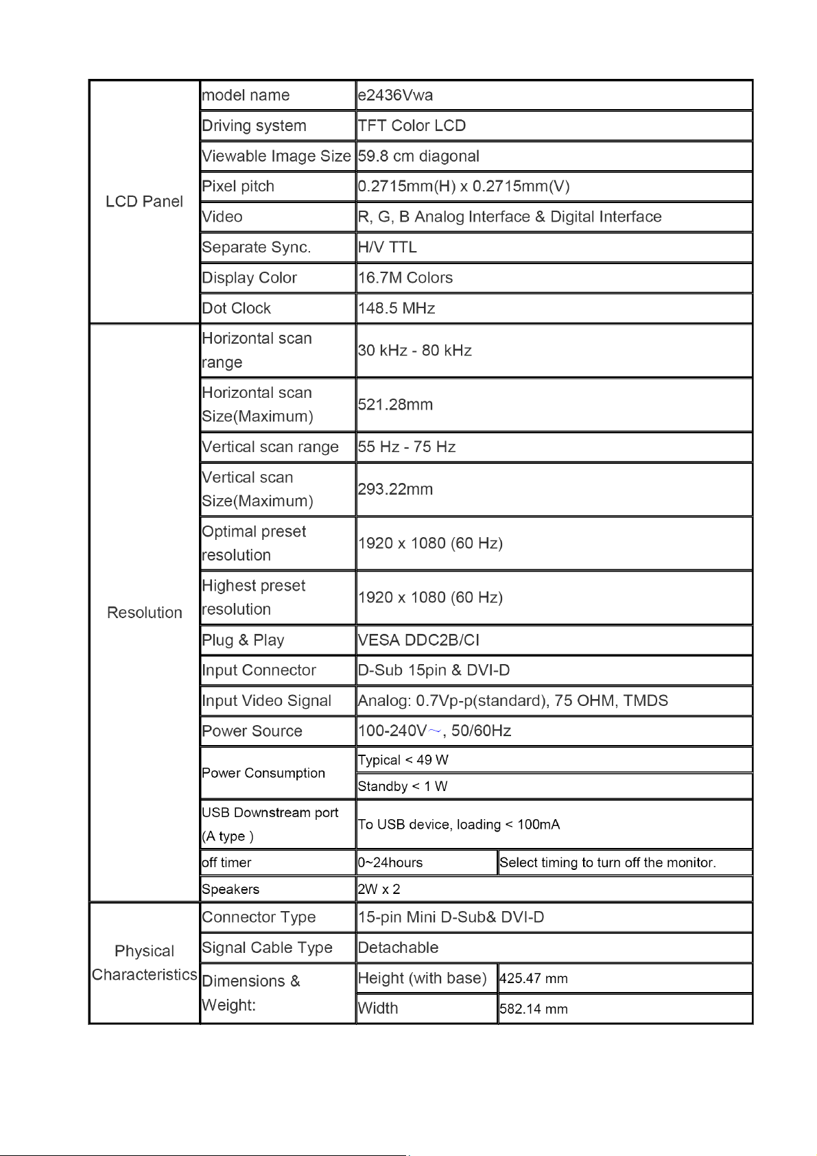
1.Monitor Specifications
4
Page 5
5
Page 6
A
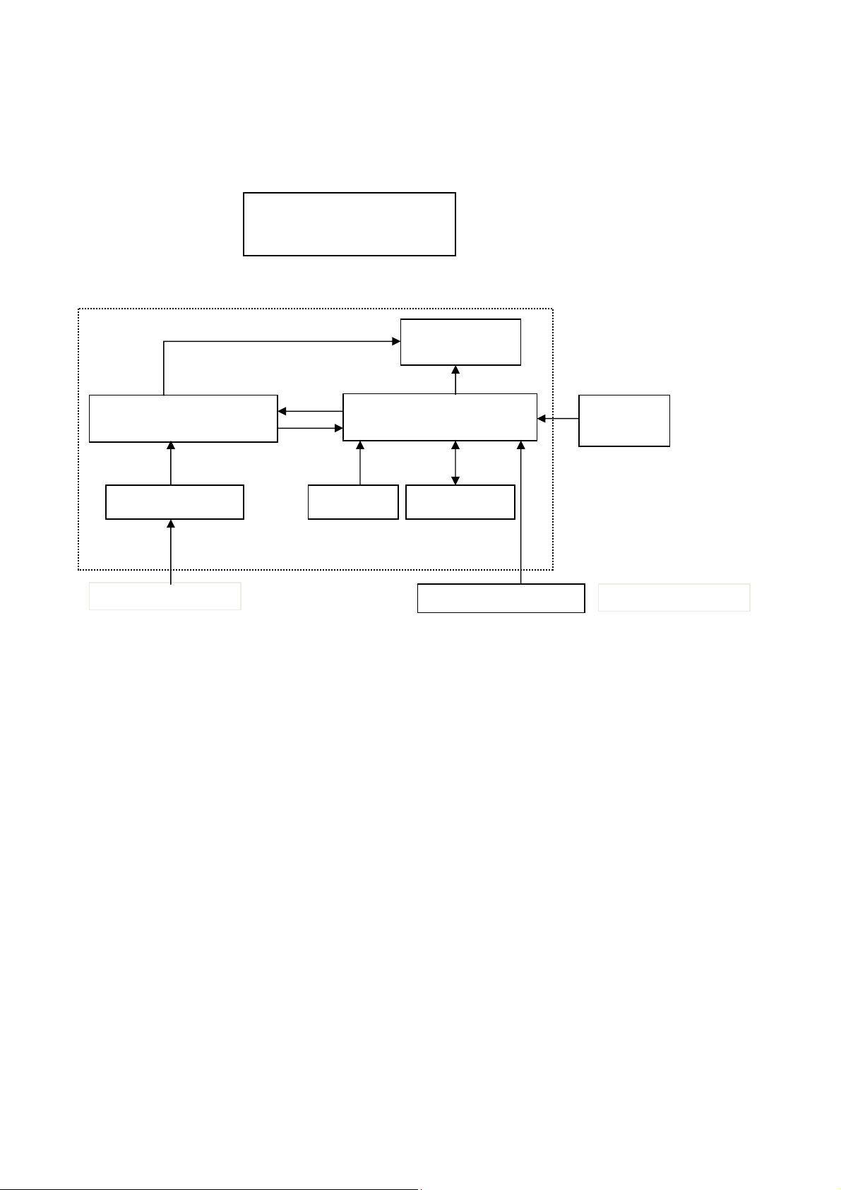
2.LCD Monitor Description
The LCD monitor will contain a main board, an adapter board, a converter board ,a key board and two USB
boards.The main board houses the flat panel control logic, brightness control logic and DDC.
The adapter board will provide AC to DC Inverter voltage to drive the backlight of panel and the main board chips
each voltage.
LED Drive
Monitor Block Diagram
Flat Panel and
LED backlight
Converter Board
Adapter Board
C-IN 90~264V
Key Board
Main Board
USB Board*2
HOST Computer
DVI-D
D-SUB
Video signal, DDC
6
Page 7
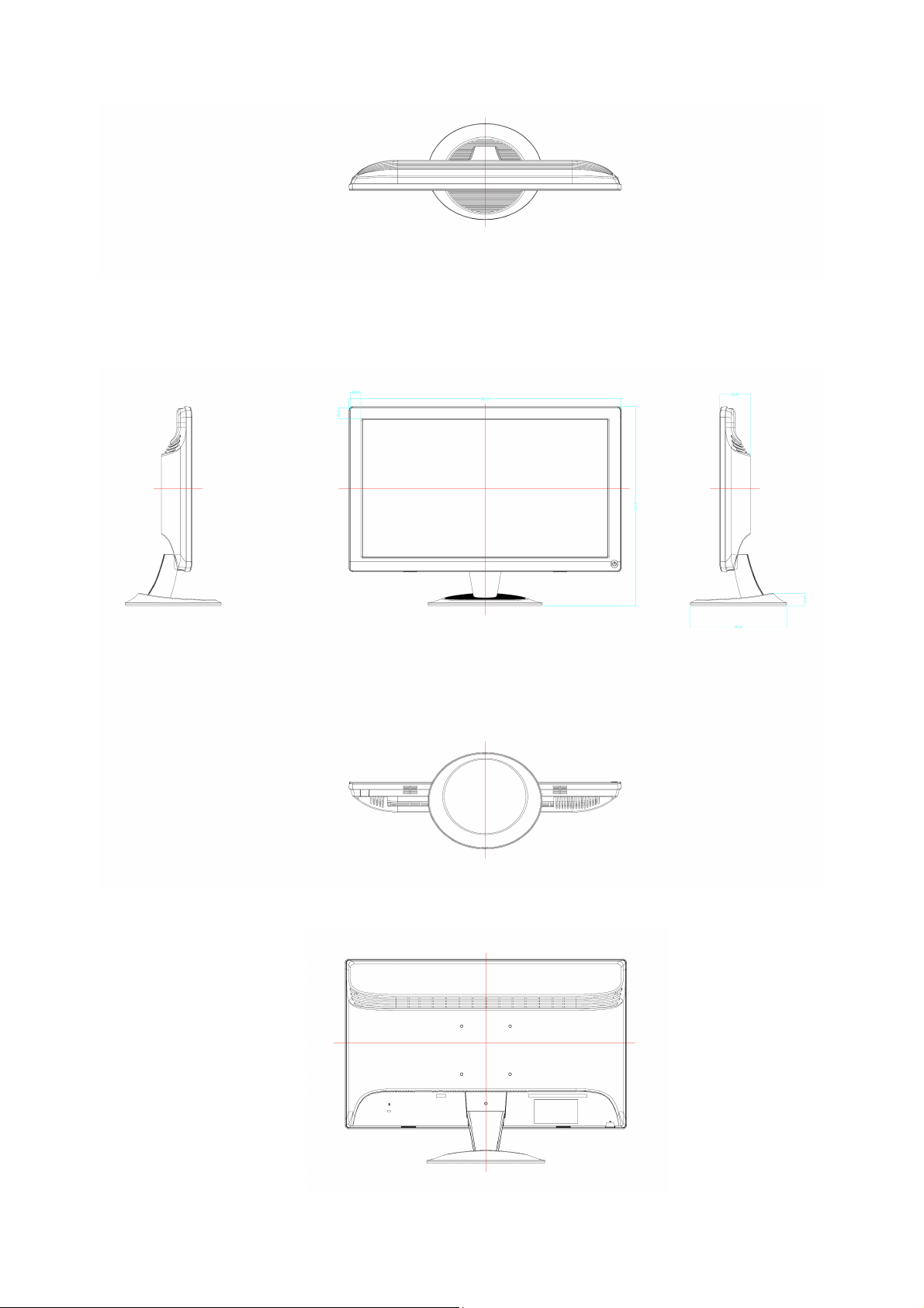
View and Dimension
7
Page 8
3. Operating Instructions
3.1 General Instructions
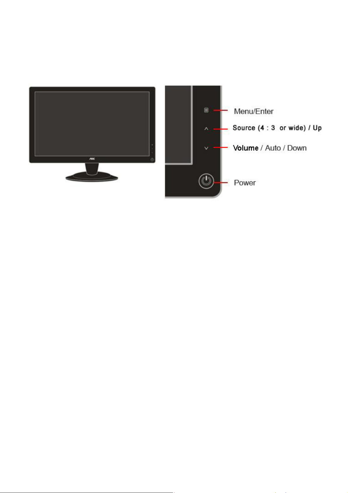
Press the power button to turn the monitor on or off. The other control knobs are located at front panel of the monitor
(See Figure ). By changing these settings, the picture can be adjusted to your personal preferences.
* The power cord should be connected.
* Press the power button to turn on the monitor. The power indicator will light up.
3.2 Control Buttons and Connections
Power Press to turn on or turn off the monitor.
Source (4 : 3 or wide)/ Up
Press∧key to change the screen aspect ratio between standard 4:3 format or Wide format. When the input
resolution is wide format, the aspect ratio hotkey is disabled. When the main menu or sub-menu is active, the∧ key
functions as to select up or increase value.
Source hot key : When the OSD is closed, press button will be Source hot key function (Only for the models with
dual or more inputs) .Press Source button continuously to select the input source showed in the message bar , press
Menu/Enter button to change to the source selected.
Menu / Enter
Press to activate OSD, then press Up or Down to navigate through the functions. Once the desired function is
highlighted, press the Menu button to activate the submenu. In sub-menu, Press Up or Down to navigate through
the functions. Once the desired function is highlighted, press Up or Down button to change the setting. Select Exit
icon then press Menu button to return to superior menu.
Volume(Auto) / Down
When there is no OSD, press the key to activate Volume and auto function, then press Up or Down to select
Volume or Auto configure function. Once the Volume icon is selected, press Menu button to activate it, and press Up
or Down to change the setting, press Menu button for confirmation and exit OSD . Once the Auto icon is selected,
press Menu button to do auto configure and exit OSD . If the product has no speaker built-in, to press the Down key
is to do auto configure directly. When it is DVI or HDMI input, auto configure function is disabled and the auto icon is
gray.
8
Page 9
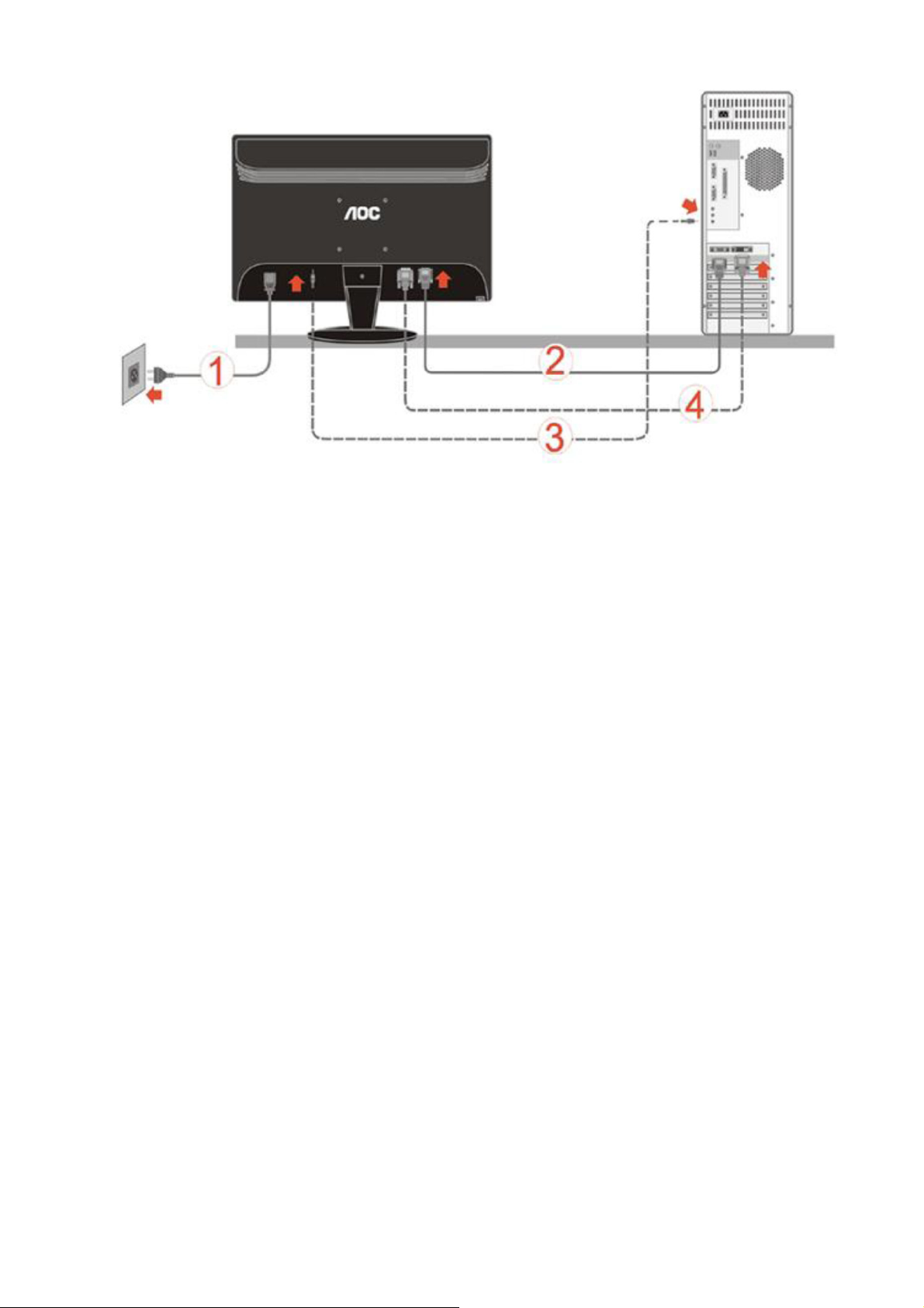
1. Power
2. Analog (DB-15 VGA cable)
3.Audio
4.DVI
To protect equipment, always turn off the PC and LCD monitor before connecting.
1 Connect the power cable to the AC port on the back of the monitor.
2 Connect one end of the 15-pin D-Sub cable to the back of the monitor and connect the other end to the computer's
D-Sub port.
3 Connect the audio cable to audio in port on the back of the monitor.
4 (Optional – Requires a video card with DVI port) - Connect one end of the DVI cable to the back of the monitor and
connect the other end to the computer‟s DVI port.
5 Turn on your monitor and computer.
If your monitor displays an image, installation is complete. If it does not display an image, please refer
Troubleshooting.
9
Page 10
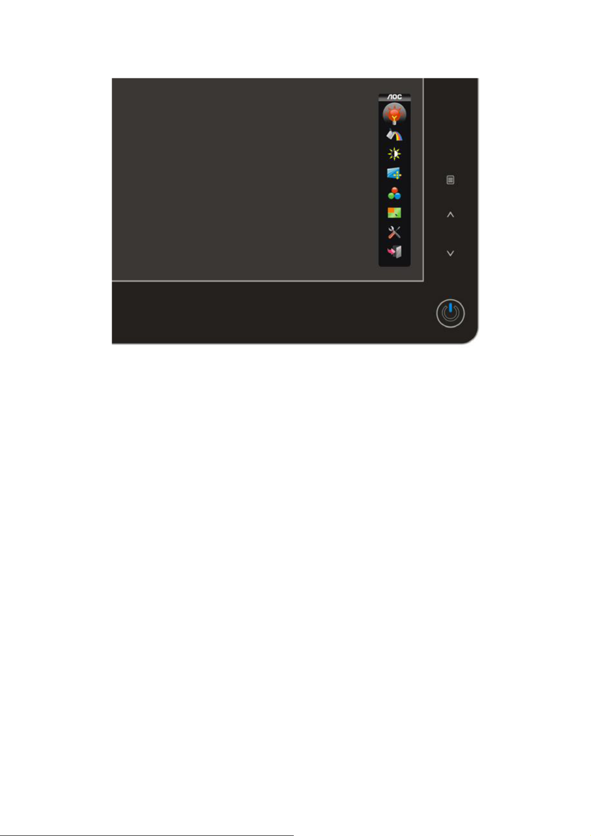
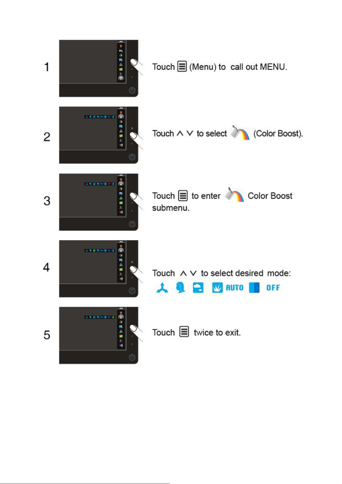
3.3 OSD Setting
Basic and simple instruction on the control keys.
When you press the MENU button on the front control of your monitor, the On DOWN Screen Display (OSD) Main
Controls window will pop up and you can then start making adjustments to your monitor's various features. Use the
UP or DOWN keys to make your adjustments. Follow the steps below to activate the adjustment.
1) Press the MENU key to activate the OSD window.
2) Press UP or DOWN to navigate through the functions. Once the desired function is highlighted, press the MENU
key to activate it. If the function selected has a sub-menu, press UP or DOWN again to navigate through the
sub-menu functions. Once the desired function is highlighted, press MENU key to activate it.
3) Press UP or DOWN to change the settings of the selected function. Press MENU key to exit and save, select the
exit function. If you want to adjust any other function, repeat steps 2-3.
4) OSD Lock Function: To lock the OSD, press and hold the MENU key while the monitor is off and then press
power button to turn the monitor on. To unlock the OSD, press and hold the MENU key while the monitor is off and
then press power button to turn the monitor on.
10
Page 11

Eco mode
11
Page 12
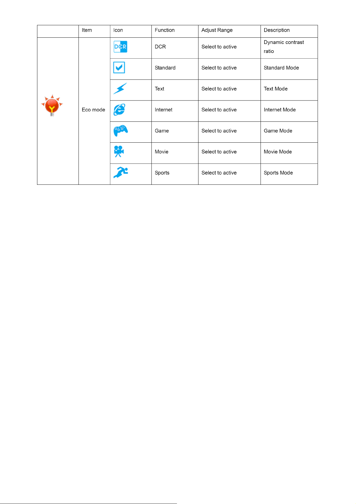
Notes :
When Eco mode is not set as “Standard”, Contrast and Brightness can not be adjusted; When DCR is set as “On”,
Contrast, Brightness, Eco mode and Gamma can not be adjusted.
12
Page 13
Color Boost
13
Page 14
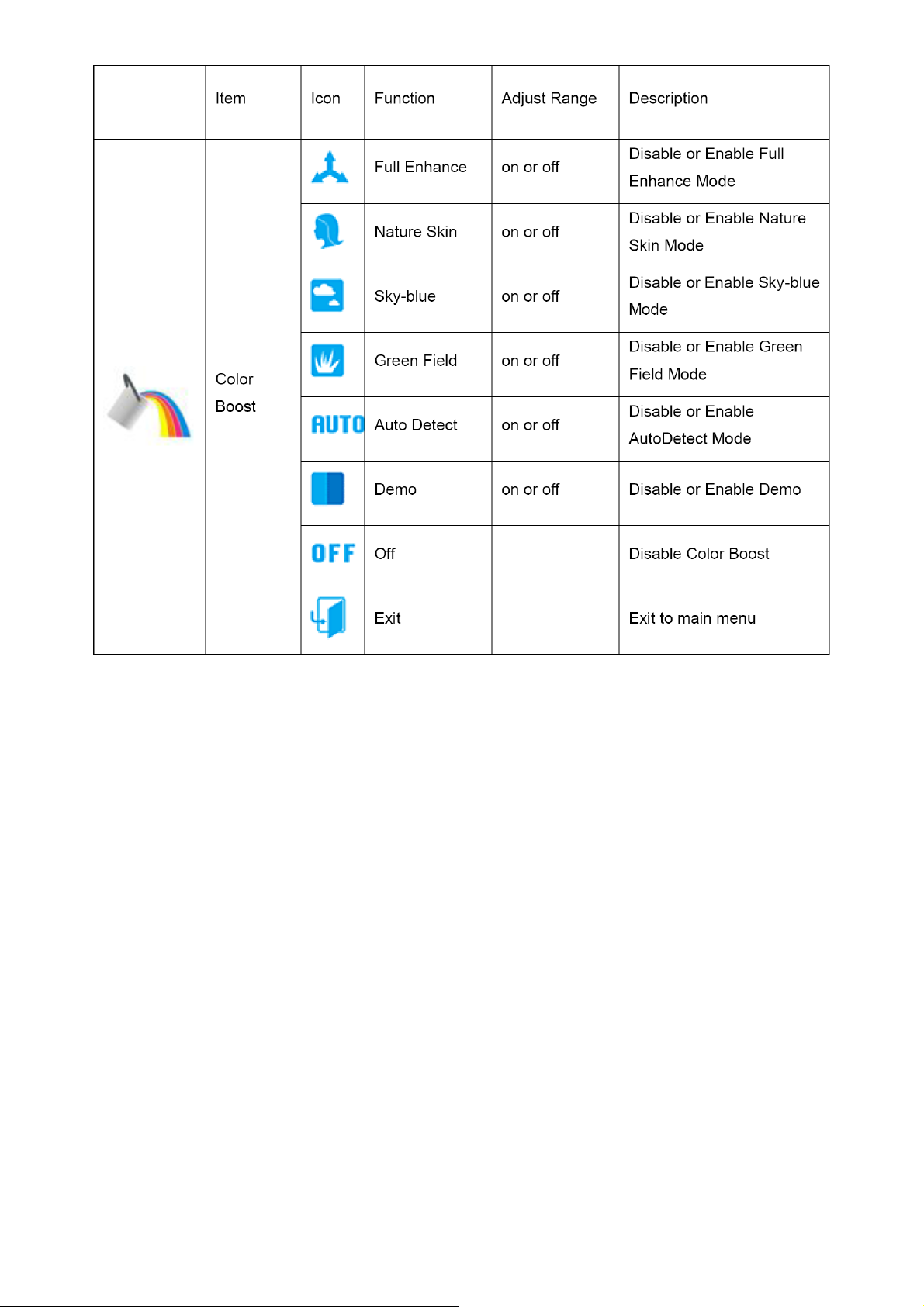
Notes :
Full Enhance: Total color saturation is enhanced, suitable for vivid pictures.
Natural Skin: Suitable for human portrait.
Green Field: Suitable for large area of green.
Sky Blue: Suitable for sky or ocean scene.
Auto Detect: Suitable for outdoor or garden.
Demo: Screen divided into two for comparison purpose.
14
Page 15
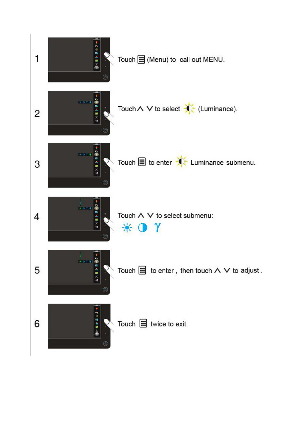
Luminance
15
Page 16
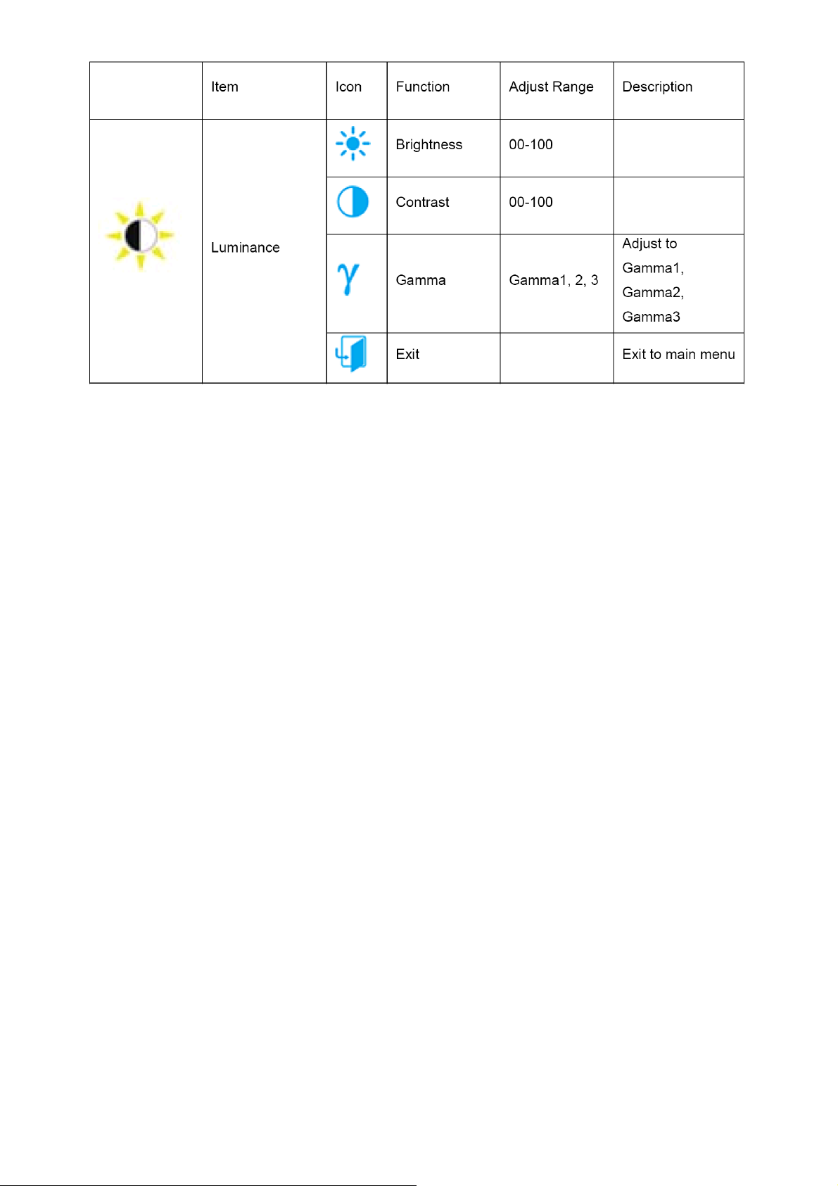
Notes :
When Eco mode is not set as “Standard”, Contrast and Brightness can not be adjusted; When DCR is set as “On”,
Contrast, Brightness, Eco mode and Gamma can not be adjusted.
16
Page 17
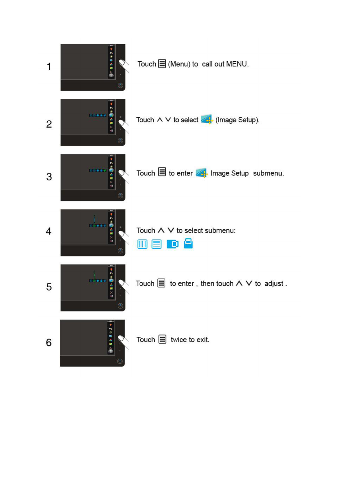
Image Setup
17
Page 18
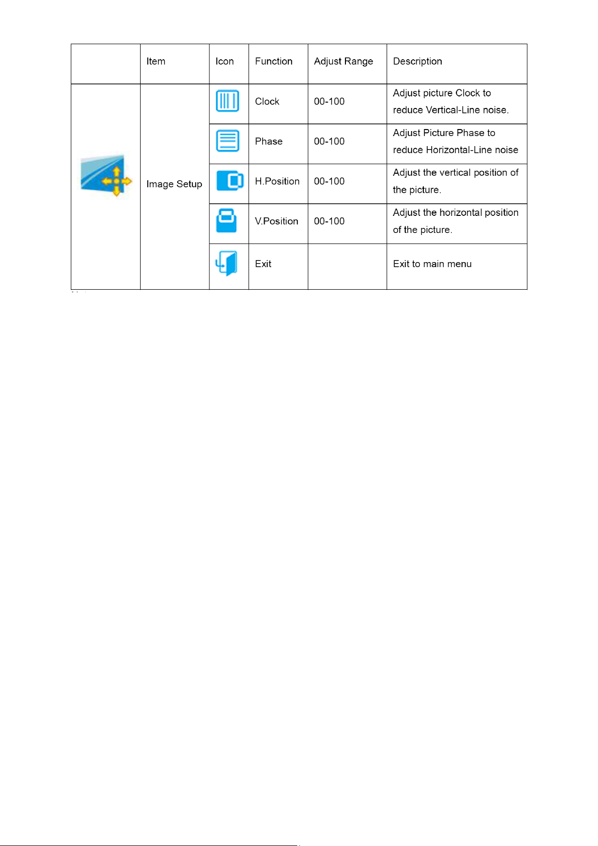
Notes :
When the input source is digital signal like DVI or HDMI, Image Setup can not be adjusted.
18
Page 19
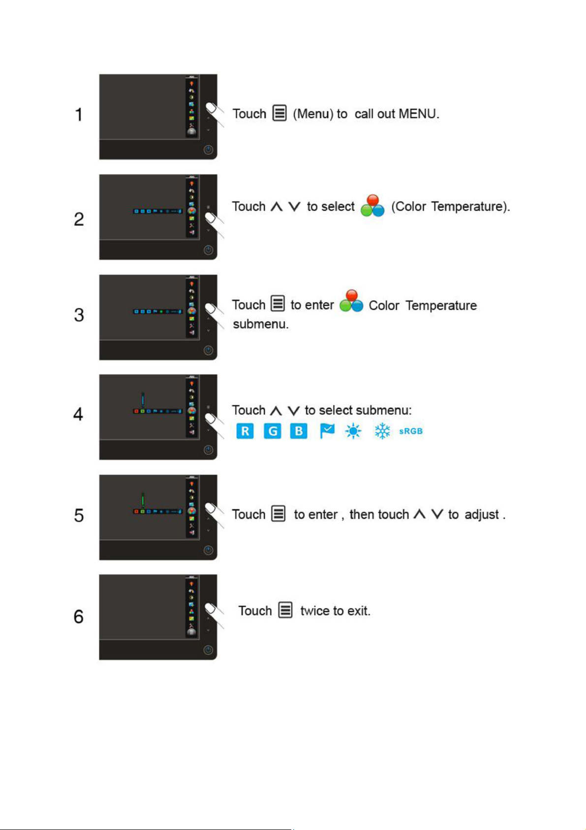
Color Temperature
19
Page 20
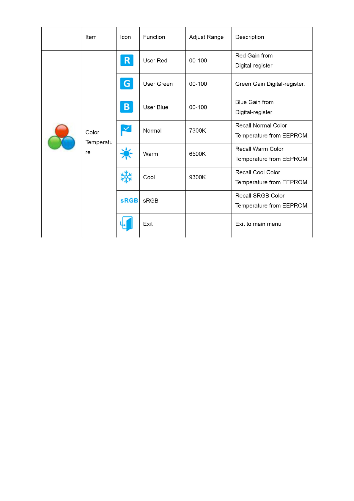
20
Page 21
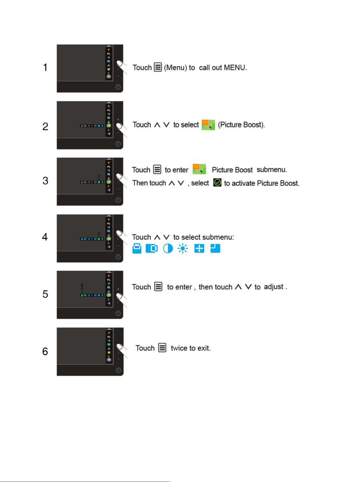
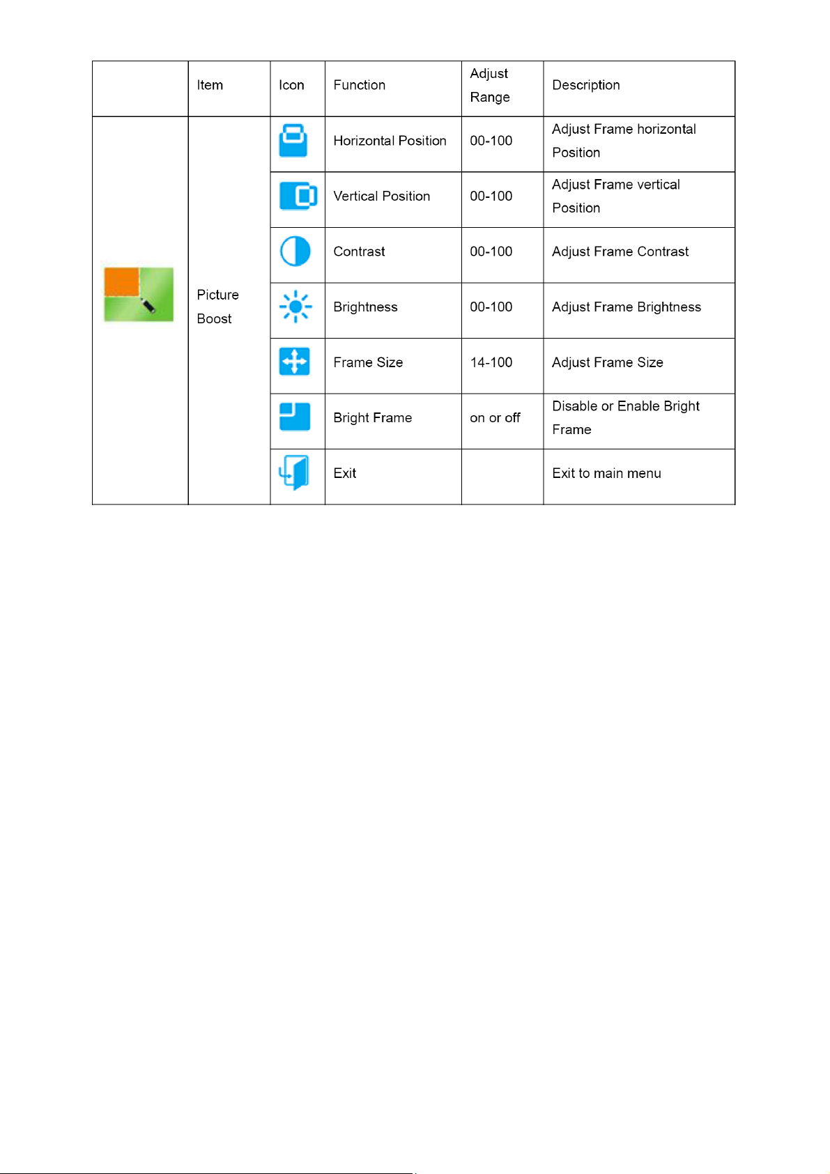
Picture Boost
21
Page 22
Notes :
One of DCR, Color Boost, and Picture Boost functions is active, the other two function is turned off accordingly.
22
Page 23
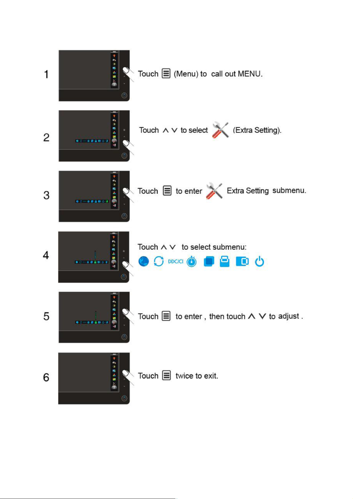
Extra Setting
23
Page 24
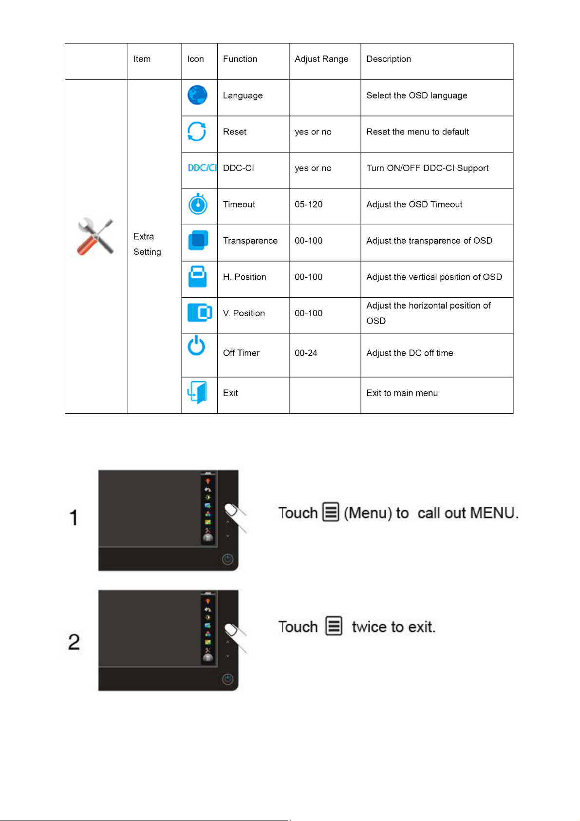
Exit
24
Page 25
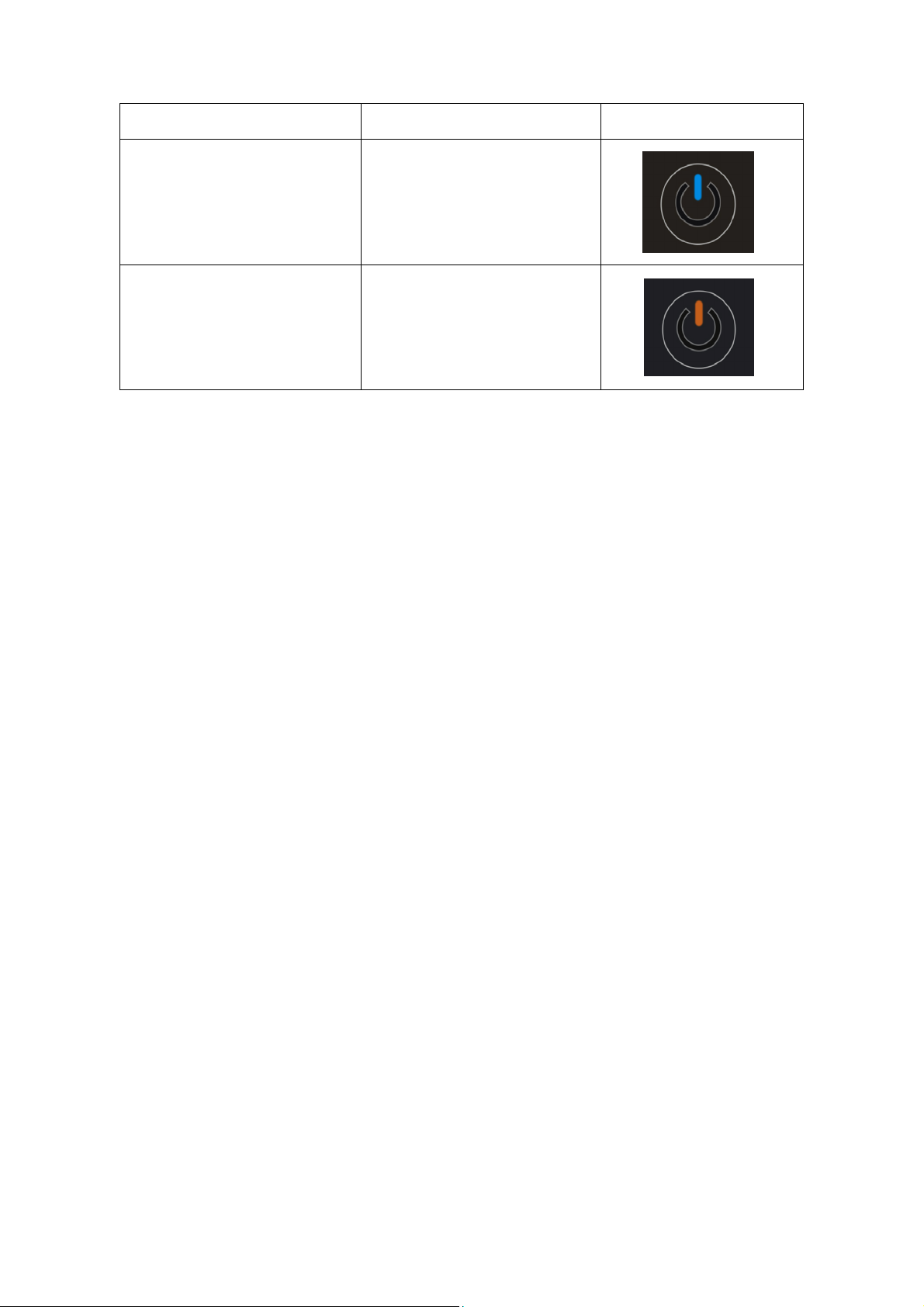
LED Indicators
Status LED Color
Full Power Mode Blue
Active-off Mode Orange
25
Page 26

4. Input/Output Specification
4.1 Input Signal Connector
Analog connector
Pin Number 15-Pin Side of the Signal Cable
DVI connector
1 Video-Red
2 Video-Green
3 Video-Blue
4 N.C.
5 Detect Cable
6 GND-R
7 GND-G
8 GND-B
9 +5V
10 Ground
11 N.C.
12 DDC-Serial data
13 H-sync
14 V-sync
15 DDC-Serial clock
Pin
No.
1 TMDS Data 2- 9 TMDS Data 1- 17 TMDS Data 0-
2 TMDS Data 2+ 10 TMDS Data 1+ 18 TMDS Data 0+
3 TMDS Data 2/4 Shield 11 TMDS Data 1/3 Shield 19 TMDS Data 0/5 Shield
4 TMDS Data 4- 12 TMDS Data 3- 20 TMDS Data 5-
5 TMDS Data 4+ 13 TMDS Data 3+ 21 TMDS Data 5+
6 DDC Clock 14 +5V Power 22 TMDS Clock Shield
7 DDC Data 15 Ground(for+5V) 23 TMDS Clock +
8 N.C. 16 Hot Plug Detect 24 TMDS Clock -
Signal Name Pin No. Signal Name
Pin
No.
Signal Name
26
Page 27

4.2 Preset Display Modes
STANDARD RESOLUTION
VGA 640×480 @60Hz 31.469 59.940
VGA 640×480 @67Hz 35.000 66.667
VGA 640×480 @72Hz 37.861 72.809
VGA 640×480 @75Hz 37.500 75.000
Dos-mode 720×400 @70Hz 31.469 70.087
SVGA 800×600 @56Hz 35.156 56.250
SVGA 800×600 @60Hz 37.879 60.317
SVGA 800×600 @72Hz 48.077 72.188
SVGA 800×600 @75Hz 46.875 75.000
SVGA 832×624 @75Hz 49.725 74.550
XGA 1024×768 @60Hz 48.363 60.004
XGA 1024×768 @70Hz 56.476 70.069
XGA 1024×768 @75Hz 60.023 75.029
XGA 1024×768 @75Hz 60.241 74.927
*** 1280×960 @60Hz 60.000 60.000
SXGA 1280×1024 @60Hz 63.981 60.02
SXGA 1280×1024 @75Hz 79.976 75.025
WXGA+ 1440×900 @60Hz 55.935 59.887
WSXGA 1680X1050 @60Hz 65.290 59.954
HD 1920×1080@60Hz 67.500 60.000
HORIZONTAL
FREQUENCY(kHZ)
VERTICAL
FREQUENCY(Hz)
4.3 Panel Specification
4.3.1 General Features
M236H3-L02 is a 23.6” TFT Liquid Crystal Display module with WLED Backlight unit and 30 pins 2ch-LVDS
interface. This module supports 1920 x 1080 Full HD mode and can display up to 16.7M colors. The converter
module for Backlight is not built in.
Features
–Extra-wide viewing angle. -High contrast ratio.
-Fast response time. -High color saturation.
-Full HD (1920 x 1080 pixels) resolution.
-DE (Data Enable) only mode.
-LVDS (Low Voltage Differential Signaling) interface.
RoHS compliance.
4.3.2 GENERAL SPECIFICATIONS
27
Page 28

4.3.3 Electrical Characteristics
1.TFT LCD Module
Vcc = 5.0 V, Ta = 25 ± 2℃, fv = 60Hz
2.Back Light Unit(LED matrix is 12S8P)
Ta = 25 ± 2℃
Note (1)LED can work normally if the PWM dinming ratio range is from 0% to 100% and the operation current
Is 25mA
Note (2) PLED = (ILED×8) ×VLED, LED matrix is 12S8P.
Note (3)The lifetime of LED is defined as the time when it continues to operate under the conditions at
Ta = 25 ± 2℃ and I = 25 mA(Per EA) until the brightness becomes ≤50% of its original value.
28
Page 29

4.3.4 Optical Characteristics
Ta = 25 ± 2℃,Ha =50±10 %RH, VCC =7V
29
Page 30

5. Block Diagram
5.1 Main Board
Keypad Interface Panel Interface
(CN402) (CN301)
Flash IC EN25F20 Scaler IC TSUMU58EHL-L Crystal
(U402) (Include ADC.OSD.MCU) NXS14.31818
(U401) (X401)
EEPROM EEPROM
AT24C02BN AT24C02BN
(U101) (U102)
DDC1-SCL DDC2-SCL
DDC1-SDA DDC2-SDA
D-Sub Connector DVI Connector
(CN101) (CN102)
30
Page 31

5.2 Power Board
Adapter
AC input Bridge Rectifier Transformer Rectifier 16V
EMI filter and Filter (T901) diodes
5V
Start Resistor
(R904,R905)
PWM Control Power Switch Feedback
LD7576(IC901) (Q901) Circuit
Photocoupler Regulator
(IC903) (IC904)
Audio
CN601(PHONE JACK)
Audio Power Amplifier
5V APA2069JITUL CN602
(IC601)
Converter
Boost Circuit 12V
LED
OVP Circuit Setup-up Controller
Panel DIM
IC TA9690G
Current Feedback (IC801,IC802) ENA
31
Page 32

6. Schematic
6.1 Main Board
715G3329 1 2
DDC1_SCL5
DDC1_SDA5
DDC 1_SCL
DDC 1_SDA
CN102
SYN C GND
JACK
GND POW ER
100R 1/16W 5%
VSYNC
DDC SCL
DDC SDA
+5V
HPD
1/3shiel d
2/4shiel d
0/5shiel d
clk shield
DAT0+
DAT0DAT1+
DAT1DAT2+
DAT2DAT3+
DAT3DAT4+
DAT4DAT5+
DAT5-
clk+
clk-
GND
GND
26
25
R101
R113
100R 1/16W 5%
8
15
DVI_HPD
6
7
14
16
11
3
19
22
18
17
10
9
2
1
13
12
5
4
21
20
23
24
DGND
H_Sync
R102 0R05 1/ 10W 5%
V_Sy nc
15
DSUB_SCL
14
13
DSUB_SDA
12
11
U107
AZC199-04S
1
I/O1
I/O4
2
GND
VDD
3 4
I/O2 I/O3
R106
2K2 1/16W 5%
CN101
17 16
ESD_VCC 1
6
5
候綼
10
5
9
4
8
3
7
2
6
1
U107
VGA_PLUG
DVI_5V
C120
NC
R107
2K2 1/16W 5%
VGA_BVGA_B+
ZD104
VGA_G-
RLZ5.6B
VGA_G+
VGA_RVGA_R+
R120 10K 1/16W 5%
C115
0.1uF/ 16V
U105
AZC199-04S
1
I/O1
I/O4
2
GND
VDD
3 4
I/O2 I/ O3
ESD_VCC 1
FB110
300 OHM
R103 1K 1/16W 5%
R104 1K 1/16W 5%
C103
C104
22pF
22pF
DSUB_SCL
DSUB_SDA
DSUB_5V
6
5
C124
0.1uF/ 16V
VGA_G+
VGA_R+
R118 100R 1/16W 5%
R119 100R 1/16W 5%
R126 10R 1/16W 5%
R127 10R 1/16W 5%
R128 10R 1/16W 5%
R129 10R 1/16W 5%
R130 10R 1/16W 5%
R131 10R 1/16W 5%
C118
NC
U105
ESD_VCC 2
U106
AZC199-04S
1
I/O1
I/O4
2
GND
VDD
3 4
I/O2 I/ O3
ESD_VCC 1 ESD_VCC 1
候綼
DSUB_H 5
DSUB_V 5
U104
AZC199-04S
1
I/O1
I/O4
2
GND
VDD
3 4
I/O2 I/O3
U103
AZC199-04S
1
I/O1
I/O4
2
GND
VDD
3 4
I/O2 I/O3
DDC2_SCL
DDC2_SDA
RX0P
RX0N
RX1P
RX1N
RX2P
RX2N
R132 10R 1/ 16W 5%
R134 10R 1/ 16W 5%
6
5
C119
NC
候綼
U106
6
5
6
5
DDC2_SCL 5
DDC2_SDA 5
RX0P 5
RX0N 5
RX1P 5
RX1N 5
RX2P 5
RX2N 5
H_Sync
V_Sy nc
VGA_PLUG
VGA_B+
RXCP
RXCN
ESD_VCC
候綼
ESD_VCC
候綼
R122
NC
DVI_HPD
VGA_PLUG
VGA_B+
VGA_B-
VGA_G+
C112
NC
U103
C101
NC
U101
DVI 1_5V
R140
NC
R121
NC
Q101
NC
RXCP 5
RXCN 5
R135
10K 1/16W 5%
6K8 1/16W 5%
T P V ( Top Victory Electronics Co . , Ltd. )
絬 隔 瓜 絪 腹
Key Component
Date
VGA_G-
VGA_R+
VGA_R-
HDCP_CTRL 5
VCC3.3
R133
10K 1/16W 5%
DET_CABLE 5R139
G3329-C-2-X-2-090401
2.0.I NPUT
FB102
1 2
BEAD
FB103
1 2
BEAD
FB101
1 2
BEAD
4K7 1/16W 5%
DDC1_SCL
DDC1_SDA
DDC_WP5
100R 1/16W 5%
R105
R108
75R 1/16W 5%
R112
75R 1/16W 5%
R116
75R 1/16W 5%
ESD_VCC
R124
R125
4K7 1/16W 5%
CMVCC1
4K7 1/16W 5%
FB104
300 OHM
C121
1000pF
ESD_VCC1
R137
DDC2_SCL
DDC2_SDA
DDC_WP5
OEM MO DE L Si ze
TPV MO DEL
PCB NAME
Sheet
C105
5pF/50V
100R 1/16W 5%
R109
470R 1/16W 5%
R110
R111
100R 1/16W 5%
C109
5pF/50V
100R 1/16W 5%
R114
100R 1/16W 5%
R115
C113
5pF/50V
R117
100R 1/16W 5%
CMVCC13,4
R123
4K7 1/16W 5%
2
3
R138
4K7 1/16W 5%
NEW R SERIES
AOC 2236VWA B
25Wednesday , June 10, 2009
of
1
D108
BAV70
R136
4K7 1/16W 5%
8
7
6
C114
8
7
6
C111
0.047uF
VCC
WP
SCL
C102
0.047uF
C106
0.047uF
C107
C108
0.047uF
C110
0.047uF
0.047uF
DVI 1_5V
VCC
WP
SCL
1000pF
CMVCC1
DSUB_5V
1
2
3
U101
1
A0
2
A1
3
A2
45
GNDSDA
AT24C02BN-SH-T
FB105
300 OHM
U102
A0
A1
A2
GNDSDA
AT24C02BN-SH -T
Rev
称爹
DSUB_B+ 5
DSUB_B- 5
DSUB_SOG 5
DSUB_G+ 5
DSUB_G- 5
DSUB_R+ 5
DSUB_R- 5
D104
BAV70
C116
0.22uF16V
DVI_5V
C122
1000pF
C117
0.22uF16V
1
2
3
45
B
称爹
>
<
32
Page 33

PA[0.. 9]5
PPWR_ON #5
PA[0.. 9]
R303
4K7 1/16W 5%
PA0
LVA3P
LVA3M
PA1
LVACKP
PA2
LVACKM
PA3
PA4
LVA2P
LVA2M
PA5
LVA1P LVBCKM
PA6
PA7
LVA1M
LVA0P
PA8
PA9
LVA0M
CMVCC12,4
R304
22K 1/16W 5%
C304
0.1uF /16V
PB[0.. 9]5
CMVCC1
R305
10K 1/16W 5%
Q302
2N3904S-RTK/PS
PB[0.. 9]
56K 1/16W 5%
1
G
R306
3
PB0
LVB3P
PB1
LVB3M
PB2
LVBCKP
LVBCKM
PB3
PB4
LVB2P
PB5
LVB2M
PB6
LVB1P
PB7
LVB1M
PB8
LVB0P
PB9
LVB0M
080912
R307
NC
D
2
S
C302
0.22uF16V
FB301
1 2
120 OHM
Q301
AO3401
C303
1uF/25V
LVB0M
LVB1M
LVB2M
LVBCKM
LVB3M
LVA0M
LVA1M
LVA2M
LVACKM
LVA3M
PANEL_VCC
C305
+
100UF25V
5
D
G
4
RXO0RXO1RXO2RXOCRXO3RXE0RXE1RXE2RXECRXE3-
876
U301
DDD
NC/ AO4411
SSS
123
R308
10K 1/16W 5%
LVB0M
RXO0-
LVB0P
CN302
9
7
5
3
1
CONN
CMVCC1
30
28
26
24
22
20
18
16
14
12
10
8
6
4
2
RXO0+
RXO1+
RXO2+
RXOC+
RXO3+
RXE0+
RXE1+
RXE2+
RXEC+
RXE3+
LVB0P
LVB1P
LVB2P
LVBCKP
LVB3P
LVA0P
LVA1P
LVA2P
LVACKP
LVA3P
PANEL_VCC
PANEL_VCC
R301
220 OHM 1/4W
R302
220 OHM 1/4W
29
27
25
23
21
19
17
15
13
11
LVB1M
LVB1P
LVB2M
LVB2P
LVBCKP
LVB3M
LVB3P
LVA0M
LVA0P
LVA1M
LVA1P
LVA2M
LVA2P
LVACKM
LVACKP
LVA3M
LVA3P
RXO0+
RXO1RXO1+
RXO2RXO2+
RXOCRXOC+
RXO3RXO3+
RXE0RXE0+
RXE1RXE1+
RXE2RXE2+
RXECRXEC+
RXE3RXE3+
C301
0.1uF/ 16V
AO3401L
CN301
30
29
28
27
26
25
24
23
22
21
20
19
18
17
16
15
14
13
12
11
10
9
8
7
6
5
4
3
2
1
NC
T P V ( Top Victory Electronics Co . , Ltd. )
絬 隔 瓜 絪 腹
Key Component
G3329-C-2-X-2-090401
3.0.OU TPUT
Date
OEM MODEL Size
TPV MO DEL
PCB NAME
Sheet
NEW R SERIES
AOC 2236VWA
of
35Wednesday , June 10, 2009
Rev
称爹
33
B
B
<
称爹
>
Page 34

CMVCC1 2,3
CN701
9
8
7
6
5
4
3
2
1
CONN
lock type
CMVCC1
CMVCC1
BKLT-VBRI
PANEL_ID #
Volume#
Mut e1
DGND 2,3,5
BKLT-VBRI
BKLT-EN
C702
0.1uF/ 16V
R710 NCBKLT-EN
Volume# 5
C701
0.1uF/ 16V
CMVCC1
R702
10K 1/16W 5%
Q701
2N3904S-RTK/PS
C712
0.1uF/ 16V
R704
22K 1/16W 5%
VCC3.3
R705
1K 1/16W 5%
VCC3.3
R703
10K 1/16W 5%
R706
100R 1/16W 5%
R709
NC
PANEL_ID # 5
Mute 5
on_BACKLIGH T 5
adj_BACKLIGH T 5
Both 223 and 252
foot-print
CMVCC1
R708
3.3OHM 2W
R701
NC
C713
0.1uF/ 16V
SOT 252
C708
0.1uF/ 16V
U704
NC/ AP1117E18LA
3 2
VI VO
GND
4
1
4
U703
AZ1117D-1. 8-E1
OUTIN
GND
1
ADJ(GND )
VOUT
VIN
123
SOT 223
VOUTVI N
VSS
1
U701
AP1117E33LA
SOT 223
23
U702
NC/ AP1117D33L-13
23
C705
0.1uF/ 16V
C709
0.1uF/ 16V
VCC1. 8
+
VCC3.3
C707
+
100UF25V
C704
100UF25V
T P V ( Top Victory Electronics Co . , Ltd. )
Date
G3329-C-2-X-2-090401
4.0.POW ER
絬 隔 瓜 絪 腹
Key Component
OEM MODEL Size
TPV MODEL
PCB NAME
NEW R SERIES
AOC 2236VWA B
of
45Wednesday , June 10, 2009
Sheet
Rev
称爹
34
B
称爹
>
<
Page 35

VDVI
AVDD
CMVCC1
0.22uF16V
MSCL
MSDA
VCC3.3
C401
R412
10K 1/16W 5%
C419
+
10UF50V
NC
SST
Eon
SST
010A
020A
Eon
020
AVDD
U402
1
8
CS#
VCC
2
7
DO
HOLD#
WP
3
6
WP#
CLK
4 5
VSS DI
U402
U402
U402
C420 47pF
C421 47pF
8
7
NC
PPWR_ON#3
U403
NC
VCC
E1
WC
E2
SCL
VSSSDA
EN25F20-100GCP
R421
100K 1/16W 5%
R442
R441NCR440
NC
EE_WP
For user data, WB, EDID,
HDCP are saved in
Flash.
Befor AOC ID2007 OSD
For ID2008 ID2009
For All model
DSUB_R+2
DSUB_R-2
DSUB_G+2
DSUB_G-2
DSUB_SOG2
DSUB_B+2
DSUB_B-2
DSUB_H2
DSUB_V2
DDC1_SDA2
DDC1_SCL2
RX2P2
RX2N2
RX1P2
RX1N2
RX0P2
RX0N2
RXCP2
RXCN2
DDC2_SDA2
DDC2_SCL2
R401 390 OHM 1/16W
0.1uF/16V
C417
R423
0R05 1/16W
X401
14.31818MHz
1 2
R428 100R 1/16W 5%
C422 0.1uF/16V
VCC3.3
1
2
3456
VMPLL
VPLL
8
14
98163249668234
23
RIN0P
AVDD_33
AVDD_33
AVDD_33
22
RIN0M
20
GIN0P
19
GIN0M
21
SOGIN0
18
BIN0P
17
BIN0M
27
HSYNC0
28
VSYNC0
30
DDCA_SD A/RS 232_TX
31
DDCA_SCL/rs232_R X
3
RX2P
4
RX2N
6
RX1P
7
RX1N
9
RX0P
10
RX0N
12
RXCKP
13
RXCKN
100
DDCD_SDA
1
DDCD_SCL
15
REXT
TSUMU58EHL-LF-1
26
REFP
25
REFM
37
SDO
38
SCZ
39
SCK
40
SDI
48
GPIO_P45/PWM1
84
RST
96
XOUT
97
XIN
80
BYPASS
52
MODE[ 0]
53
MODE[ 1]
GND
2
5
X'TAL
Normal Function : CL = Cs + ((Cg*Cd)/(Cg+Cd))
C423
P.S : Assume Cs = 4 pF
NC
蔼
瑉红
U403
C423
R429
R430
R440
R442
VDDC
VDDP
24
56
51
75
VDDP
VDDP
VDDP
VDDP
AVDD_33
AVDD_33
LVDS
GND
GND
GND
GND
GND
GND
GND
GND
GND
112933
5057767983
X401
(93G 22-53B-H)
(93G 22-53-J)
For NVRAM
M24C04-WMN6TP R419
0.22uF16V
100R 1/16W 5%
100R 1/16W 5%
10K 1/16W 5%
10K 1/16W 5%R441
10K 1/16W 5%
VDDC
VDDC
VDDC
VDDC
LVACKP
LVACKM
LVBCKP
LVBCKM
GPIO_P23
GPIO_P43
GPIO_P42
GPIO_P47
GPIO_P46
GPIO_P22/PWM0
PWM2/GPIO_P24
GPIO_P25
PWM3/GPIO_P27
GPIO_P00/SAR0
GPIO_P01/SAR1
GPIO_P02/SAR2
GPIO_P03/SAR3
GPIO_P07
GPIO_P15
PWM1/GPIO_P16
GPIO_P12
GPIO_P13
GPIO_P14/PWM0
GPIO_P10/I2C_MCL
GPIO_P11/I2C_MDA
Without NVRAM
NC
NC
NC
NC
NC
NC
NC
81
VCTRL
54
LVA3P
55
LVA3M
58
59
60
LVA2P
61
LVA2M
62
LVA1P
63
LVA1M
64
LVA0P
65
LVA0M
67
LVB3P
68
LVB3M
69
70
71
LVB2P
72
LVB2M
73
LVB1P
74
LVB1M
77
LVB0P
78
LVB0M
36
45
46
41
42
35
47
85
86
87
88
89
90
91
92
93
94
95
99
44
43
CL of SPEC
PA0
PA1
PA2
PA3
PA4
PA5
PA6
PA7
PA8
PA9
PB1
PB2
PB3
PB4
PB5
PB6
PB7
PB8
PB9
R425 NC
R445 NC
R409 100R 1/16W 5%
R415 100R 1/16W 5%
R416 100R 1/16W 5%
R417 100R 1/16W 5%
R419 0R05 1/16W
R420 NC
R424 100R 1/16W 5%
R426 NC
R429 NC
R430
NC
18 pF
32 pF
PA[0..9]
PA[0..9] 3
PB[0..9]PB0
PB[0..9] 3
POWER_KEY#
EE_WP
PANEL_ID# 4
WP
on_BACKLIGHT 4
adj_BACKLIGHT 4
KEY1
KEY2
DET_CABLE 2
LED G_B
LED O
HDCP_CTRL 2
27 pF
56 pF
Indirect LED
10K 1/16W 5%
10K 1/16W 5%
0R 1/16W 5%
2.2K 1/16W 5%
NC
0R 1/16W 5%
2.2K 1/16W 5%
NC
2N3906S
2N3906S
Mute 4
BUZZER
MSCL
MSDA
Cs and Cd (C420, C421)
R420
R453
R455
R461
R457
R459
R462
Q407
Q408
R402
1K 1/16W 5%
R404 1K 1/16W 5%
100R 1/16W 5%
Max condition for LED:
1. Vcc = 3.3 V
2. Current = 12 mA
FW need to be
modified.
Direct LED
100R 1/16W 5%
100R 1/16W 5%
0R 1/16W 5%
0R 1/16W 5%
DVI 1_5V
R447
NC
CMVCC1
R422
NC
NC
NC
NC
NC
NC
1
For detect function,
depend on FW
R446
NC
R406
22K 1/16W 5%
R427
NC
R434
0R05 1/16W
R451 NC
R452 0R05 1/16W
23
Q405
2N3906S-RTK/PS
R405 0R05 1/10W 5%
CMVCC1
VCC3.3
R407
10K 1/16W 5%
C438
NC
LED G_B
CN401
NC/CONN
CN402
CONN
6
5
4
3
2
1
7
6
5
4
3
2
1
LF_B
Volume# 4
C416
0.1uF 16V
R455 NC
R461
0R05 1/10W 5%
Q401
LMBT3904LT1G
Q407
NC
NC/CONN
DDC_WP 2
R453 NC
R454 NC
R456
22R 1/16W 5%
2
4
6
8
NC/CONN
CN405
CN403
CN404
NC/CONN
VCC3.3
LED_GRN/BLUE
1
3
5
7
1
2
3
4
5
6
1
2
3
4
5
6
7
VCC3.3
VCC3.3
CMVCC1 2
CMVCC1
TOUCH_POWER
FB402
300OHM
R408
R411
R414
0R05 1/16W
LED_ORANGE
R418
0R05 1/16W
FB404
300OHM
0.1uF/16V
VCC3.32,4
NC
NC
LED_GRN/BLUE
R435
VPLL
VCC3.3
AVDD
FB401
300OHM
C408
0.1uF/16V
VMPLL
C413
VCC3.3
VCC1.84
R459 NC
LED O
POWER_KEY#
C431
NC
NC
R436
10K 1/16W 5%
VCC3.3
FB405
NC
LF_B
C436
1uF 10V
VCC1.8
C402
4.7uF/10V
R462
NC
C407
0.1uF/16V
VCC3.3
VDVI
FB410
300OHM
C415
C414
0.1uF/16V
0.1uF/1 6V
VDDP
VDDC
C433
0.1uF/16V
0.1uF/16V
R457 NC
R458 NC
R460
NC
NC
NC
NC
C406
C404
C405
0.1uF/16V
0.1uF/16V
C412
C409
0.1uF/16V
C411
C410
0.1uF/ 16V
0.1uF/16V
CMVCC1
VCC3.3
LED_ORANGE
VCC3.3
R433
R432
3.9K OHM +-1% 1/16W
3.9K OHM +-1% 1/16W
KEY1
KEY2
C435
C434
ZD401
BUZZER
CMVCC1
NC
CN406
1
2
3
NC/CONN
NC
For BUZZER control board
or Touch Panel
C403
0.1uF/16V
Q408
NC
R431
C432
0.1uF/16V
T P V ( Top Victory Electronics Co . , Ltd. )
G3329-C-2-X-2-090401
絬 隔 瓜 絪 腹
Key Component
5.0.SCALER
Date
OEM MOD EL Si ze
NEW R SERIES
TPV MODEL
AOC 2236VWA B
PCB NAME
of
Sheet
55Wednesday, J une 10, 2009
Custom
Rev
称爹
>
<
称爹
35
Page 36

6.2 Power Board
Adapter
715G2824P01010001S
1
BD901
+
!
-
4
C904
0.22UF 275V
2
3
L901
27mH
1
4
C903
0.22UF 275V
1 MOHM +-5% 1/4W
!
C901
1000pF
3
12
2
GBU408
R901
!
1
2
GND1
GND
!
!
67G315Z12115K
120uF450V
12
t
F901
FUSE
!
3
!
!
R902
1 MOHM +-5% 1/4W
!
C902
1000pF
CN901
SOCKET
GND2
GND
1
2
NR901
NTCR
C905
C940
47nF 50V
+
1500PF2KV
C928
10nF 50V
HS3
HEAT SINK(D906)
1
2
C938
NC
IC901
1
CT
2
COMP
3
CS
4 5
GNDOU T
LD7576
CN801
5
4
3
2
1
CONN
VCC
+
C918
680uF25V
L904
Coil
L903
R924
100 OHM 1/8W
C934
1000uF25V
Coil
C915
+
470UF M 16V
L905
Coil
+
OEM MOD EL Size
TPV MOD EL
PCB NAME
Sheet
R918100 OHM 1/4W
R919100 OHM 1/4W
R920100 OHM 1/4W
!
FB902
0R05 4A 1/4W
R904
8.2K 1/4W
R905
8.2K 1/4W
C907100N 50V
8
HV
7
NC
6
+16V
+
DIM
ON/OF F
CN802
5
4
3
2
1
CONN
HS2
HEAT SINK(D908)
1
2
+
D903 1N4148
R910
10 OHM 1/4W
R912
220 OHM 1/4W
C909
220pF 50V
+16V
C910
100uF 50V
C906
1500PF2KV
C908
22uF 50V
STP10NK70ZF P
NC
1
2
D901
FR103
Q901
R938
10KOHM +-5% 1/8W
R914
0.39 OHM 2W +-5%
CN903
1
2
3
4
CONN
HS1
HEAT SINK(Q90 1)
R903
100KOHM +-5% 2WS
R909
3.3 OHM 1/4 W
D900
FR107
C937
100PF1KV
!
+5V
DIM
ON/OF F
PID
VOL
MUTE
+5V1
4
POWER X'FMR
5
6
1
3
!
C921
1000pF
C900
3300pF 250V
T901
IC903
PC123X2YFZOF
43
C931
100N 50V
8
7
9
10
12
11
1K 1/8W
12
R925
C924
100N 50V
IC904
KIA431A-AT/P
12
R926
1K 1/10W
C912
1000pF630V
D906
2
FMX-12SL
3
R935 100 OHM 1/4W
R961 100 OHM 1/4W
R962 100 OHM 1/4W
D909
31DQ06FC3
D907
31DQ06FC3
FB901
BEAD
R949 100 OHM 1/4W
R950 100 OHM 1/4W
R951 100 OHM 1/4W
2
3
CN902
1
2
3
4
5
6
7
8
9
10
11
12
13
Wire Harness
C917
+
680uF25V
1
C929
1000pF630V
+
C939
1000uF M 16V
C935
1000pF630V
1
D908
MBRF1060CT
+
C916
NC
T P V ( Top Victory Electronics Co . , Ltd. )
G2824-P0A-010-0010-1-091028
絬 隔 瓜 絪 腹
Key Component
03.POWER
Date
820 OHM 2W
R947
C932
1N 50V
ZD902
TZX18B
R943
470OHM +-5% 1/8W
R939
1K 1/8W
L906
2.2uH
C930
100N 50V
R927
10K +-1% 1/10W
R930
9.1KOHM +-1% 1/10W
F902
FUSE
Rev
称爹
R946
820 OHM 2W
Q903
KTD1028
e2436vwa
ADPC91603H D1 1
715G2824-P0A-010-0010
of
23Wednesday , Oct ober 28, 2009
R940
NC
+16V
F903
FUSE
+5V1
Custom
OD M MOD EL
+5V
36
Page 37

+5V1
C603 0.47uF 16V
+
LOUT-
VDD
LOUT+
GND
GND
ROUT+
VDD
ROUT-
C602 0.47uF 16V
4
3
2
1
CN602
CONN
10
11
12
13
14
15
16
LOUT+
LOUT-
ROUT-
ROUT+
CN601
PHONEJ ACK
+5V1
VOL
4
Lin
5
3
2
1
R604 10K 1/10W 5%
Rin
R605 10K 1/10W 5%
R602
10K 1/10W
R603
10K 1/10W
C609
1U 25V
C601 0.47uF 16V
C606 0.47uF 16V
10K 1/10W
R609
+5V1
C604
100uF 25V
IC601
8 9
SE/BTL
7
VOLUME
6
LIN -
5
GND
4
GND
3
RIN-
2
BYPASS
1
SHUTDOWN
APA2069JI TUL
R608
0R051/8W
FB602
1 2
BEAD
HS4
HEAT SINK(I C601)
1
2
C610100pF 50V
C612
6.2K 1/10W
R606
6.2K 1/10W
R607
C611100pF 50V
MUTE
R612
D601
10 OHM 1/10W
1N4148
1K 1/10W
C613
+
100uF 25V
R613
Q607
PMBS3906
Q608
10K 1/10W
R610
R611
56K1/10W
MMBT 3904
100N16V
R601
10K 1/10W
C614
100N16V
C608
1U25V
IC with Heat-sink(90G6295-3)
T P V ( Top Victory Electronics Co . , Ltd. )
絬 隔 瓜 絪 腹
Key Component
Date
G2824-P0A-010-0010-1-091028
03.AUDIO
OEM MODEL Size
TPV MODEL
PCB NA ME
Sheet
e2436vwa
ADPC91603H D1 1
715G2824-P0A-010-0010
of
33Wednesday , October 28, 2009
Rev
称爹
Custom
OD M MO D EL
37
Page 38

Converter
715G3918P03000004C
CN801
CONN
CN802
CONN
5
4
3
2
1
1
2
Τэ
OVP2
OVP1
+12V
DIM
ENA
Vout
R822
1M 1/10W 5%
R823
4.7K 1/ 10W
R824
43KOHM +-1% 1/10W
F801
100N 50V
R825
0R05 1/4W
FUSE
C801
0.15 OH M +-1% 1/4W
R844 NC
+
C813
100uF 50V
R801
C812
100p 50V X7R
Iout
R804
R842
R815
R843
L801
22uH
1
2
3
4 5
APM8005KCTRG
25mA
20mA
56K
27K
56K
150K
56K
27K
56K
150K
C811 NC
S1
D1
G1
D1
S2
D2
G2 D2
Q801
100 OHM 1/10W
R802
NC
8
7
6
R845
ZD801
B360B
C803
100N 50V
10K 1/10W 5%
10K 1/10W 5%
100uF 50V
C814
100P 50V
R806
R817
+
C804
+
C810
100uF 50V
R804
30K +-1% 1/10W
N.C
R842
R815
30K +-1% 1/10W
R843 N.C
R816 160KOH M +-1%1/10W
T P V ( Top Victory Electronics Co . , Ltd. )
絬 隔 瓜 絪 腹
Key Component
Date
OVP1
R805 160KOH M +-1%1/10W
10R 1/ 10W 5%
OVP2
G3918-P0E-000-0040-1-091215
02.CON VERTER
1
PWM
STATUS
2
ISEN1
3
ISEN2
SSTCMP
4
ISEN3
5
6
7
8
9
10
11
12 13
R807
1
2
3
4
5
6
7
8
9
10
11
12 13
COMP
ISEN4
GNDA
ISEN8
GNDP
ISEN6
VREF
ISEN7
OVP
ISEN5
ISET
RT ENA
IC801
TA96 90G N
R814
10 OHM 1/10W
PWM
STATUS
ISEN1
ISEN2
SSTCMP
ISEN3
COMP
ISEN4
GNDA
ISEN8
GNDP
ISEN6
VREF
ISEN7
OVP
ISEN5
ISET
RT ENA
IC802
TA9690GN
LDR
ISW
LDR
ISW
R833 1 OH M 1/10W
R832 1 OH M 1/10W
R831 1 OH M 1/10W
R830 1 OH M 1/10W
R829 1 OH M 1/10W
R813 10K 1/10W 5%
R812
C805
0.47uF 16V
1K 1/10W 5%
R808
NC
C808
0.47uF 16V
R803
1K 1/10W 5%
R818
NC
C809
2.2U 16V
R828 1 OH M 1/10W
R827 1 OH M 1/10W
R826 1 OH M 1/10W
R810
C807
2.2U 16V
R809
100K 1/10W 5%
R839 1 OH M 1/10W
R838 1 OH M 1/10W
R837 1 OH M 1/10W
R836 1 OH M 1/10W
R835 1 OH M 1/10W
R834 1 OH M 1/10W
24
23
NC
22
21
20
SEL
19
VIN
18
17
16
15
14
24
23
NC
22
21
20
SEL
19
VIN
18
17
16
15
14
OEM MO DE L Size
TPV MODEL
PCB NAME
Sheet
100 OHM 1/10W
C806
2U2 25V
R811
0R05 1/ 10W
R821 10K 1/ 10W 5%
100 OHM 1/10W
AOC E2436VWA
LNPC9D432MHD 1
715G3918-P0E-000-0040
22Wednes day , D ecem ber 16, 2009
of
R820
R841 1 OH M 1/10W
R840 1 OH M 1/10W
R819
100K 1/10W 5%
Rev
称爹
Vout
CN803
CONN
A4
ver.E
ODM MODEL
CN805
NC
CN804
CONN
10
9
8
7
6
5
4
3
2
1
11 12
12
11
10
9
8
7
6
5
4
3
2
1
13 14
10
9
8
7
6
5
4
3
2
1
11 12
38
Page 39

7. PCB Layout
7.1 Main Board
715G3329 1 2
39
Page 40

7.2 Power Board
Adapter
715G2824P01010001S
40
Page 41

41
Page 42

Converter
715G3918P03000004C
7.3 Key Board
715G3371 2
42
Page 43

7.4 USB Board
715G3501 2
715G2663 2
43
Page 44

8. Maintainability
8.1 Equipments and Tools Requirement
1. Voltmeter.
2. Oscilloscope.
3. Pattern Generator.
4. DDC Tool with an IBM Compatible Computer.
5. Alignment Tool.
6. LCD Color Analyzer.
7. Service Manual.
8. User Manual.
44
Page 45

8.2 Trouble Shooting
1. No Power
No power
Check power cable is
tightened?
OK
Check Power “On/Off”
is “On”?
OK
Check the LED
indicate is OK?
NG
Re-plug the power cable
NG
Turn on the Power “On/Off” switch
NG
Check the AC power
OK
Replace the converter board
NG
Replace main board and check connections
NG
Replace key board and check connections
45
Page 46

2. No Video (Power LED Blue)
No Video (Power LED Blue)
Press the power
button is OK?
OK
Replace the converter
board
NG
Replace the main
board and connection
NG
Replace the main board
OK
The end
OK
The end
NG
Check the LVDS/FFC
cable or panel
NG
Replace the key board
OK
Replace the LVDS/FFC
cable or panel
46
Page 47

3. DIM
DIM (image overlap, focus or flicker)
Reset in factory mode
NG
OK
The end
Set to the optimal
frequency, select the
recommended frequency
NG
Readjust the phase and pixel
clock in the user mode
NG
Pull out signal cable and
check “Self Test Feature
Check” is ok?
OK
The end
OK
The end
OK
Check the signal cable
and the PC
NG
Replace the main board
NG
Replace the panel
OK
NG
OK
The end
47
Page 48

4. Color is not optimal
Miss color
Replace the signal cable
NG
Pull out the signal cable
and check the screen
color display is normal?
NG
Replace the main board
Replace the signal cable or PC
Color is not optimal
OK
The end
OK
Color shift
Reset the factory mode
NG
In the user mode, set the” color
settings” until customer satisfy
NG
48
Page 49

9. FOS Testing
9.1 Brightness Measurement
Max. Brightness>250 cd/㎡(typ).
Test conditions:
- Center of display
- Video input (RGB) = 0,700V for Analog Input
- Brightness control is set to max
- Contrast control is set to max.
Min. brightness measurement:
< 45% of Max luminance (max luminance = max contrast + max brightness)
Test conditions: - Center of display
- Video input (RGB) = 0.700V for Analog Input
- Brightness control is set to min.
- Contrast control is set to min.
9.2 Patterns Testing
Condition
Item
(Resolution, Commended
test paten)
Normal picture Abnormal Picture
Waterwave
noise
Mura
LCD
bubble
1. 1920 x 1080 (60 Hz)
2. White pattern
1. 1920 x 1080 (60 Hz)
2. Black pattern or White
pattern.
1. 1920 x 1080 (60 Hz)
2. Black pattern or White
pattern
49
Page 50

Cross line
Half line
1. 1920 x 1080 (60 Hz)
2. Black pattern
1. 1920 x 1080 (60 Hz)
2. Black pattern or White
pattern
H-Line
V-Line
1. 1920 x 1080 (60 Hz)
2. Black pattern, Red
pattern, Green pattern or
Blue pattern.
1. 1920 x 1080 (60 Hz)
2. Black pattern or White
pattern
H-Strip
1 1920 x 1080 (60 Hz)
2. Black pattern, Gray scale
pattern, Red pattern, Green
pattern or blue pattern .
50
Page 51

V-St rip
1. 1920 x 1080 (60 Hz)
2. Black pattern, Gray scale
pattern, Red pattern, Green
pattern or blue pattern .
Abnormal
display
Gray defect
1. 1920 x 1080 (60 Hz)
2. Gray scale pattern
1. 1920 x 1080 (60 Hz)
2. Gray scale pattern
Video noise
Color tint
1. 1920 x 1080 (60 Hz)
2. Gray scale pattern
1. 1920 x 1080 (60 Hz)
2. Gray scale pattern
51
Page 52

Gray scale
failure
Light
leakage
Fuzzy
video
1. 1920 x 1080 (60 Hz)
2. Gray scale pattern
1. 1920 x 1080 (60 Hz)
2. Black pattern or White
pattern
1. 1920 x 1080 (60 Hz)
2. Pane picture
52
Page 53

10. Firmware and DDC Instruction
10.1Firmware Instruction(TSUM IC ISP for exemple TSUMO58GDJ)
1. OPERATION CONDITIONS:
1) An i486 (or above) personal computer or compatible.
2) Microsoft operation system Windows XP.
3) “MSTAR ISP Tool V4.5.0.7.7”programs.
4) Printer cable and VGA cable.
5) ISP board (PN: 715GT039-A).
2. Connection:
1) LPT cable connect PC and ISP board ;
2)VGA cable connect monitor and ISP board ;
3)Reference picture as below
ISP Board (TPV P/N:715GT039-A)
3.Software list:
1)LPT driver:
2)MSTAR ISP TOOL:
Eg: TSUMO58GDJ_LGLM215WF4_20100518_V005_8143.BIN
3)Setup LPT driver:run Port95nt icon:
4)USB driver install
53
Page 54

4 .Program:
1)Run MSTAR ISP Tool V4.5.0.7.7,interface as below:
2) Choose CONFIG icon ,interface as below :
Setting as :
Port type :LPT1
Speed :50KHZ
54
Page 55

3)Choose DEVICE,and choice WP Pin pull to high during ISP :
4)Choose CONNECT icon ,and interface show Device type , PC and monitor communications successful, click
“OK”.
55
Page 56

5)Click “Read”, show as follow picture, then choose correct software to click “open.
PS:For exemple TSUMO58GDJ_LGLM215WF4_20100518_V005_8143.BIN
6 )Then ,as below :
7.
56
Page 57

7) Show the interface as follows after press the AUTO button
8).Then , press Run icon ,as below,Show Blank OK, Program OK, Verify OK, It’s successfully if interface show
PASS.
57
Page 58

9) AC off, wait about one minute, after the elextricity large capacitance of power board release, then AC on,
otherwise, the key button and power button cann't work.
5.Check Software Version and auto color and reset:
You should check the program code is right in factory mode ;(about the method of enter factory mode ,pls reference
the service manual )
5.1Auto level :
1)Monitor display gray pattern ;
2)Enter the factory mode ;
3)Choise the AUTO LEVEL icon and run it.
4)Check the gray pattern is clear ;
5)Change to full black pattern , and check the display there is no noise .
5.2Reset
Monitor would change to default setting after reset .
5.3power off
Monitor must be turned off after rework code.
58
Page 59

10.2 DDC Instruction(For exemple:Philips 201B)
General
DDC Data Re-programming
In case the main EEPROM with Software DDC which store all factory settings were replaced because a defect
repaired monitor’ the serial numbers have to be re-programmed.
It is advised to re- soldered the main EEPROM with Software DDC from the old board onto the new board if circuit
board have been replaced, in this case the DDC data does not need to be re-programmed.
Additional information about DDC (Display Data Channel) may be obtained from Video Electronics Standards
Association (VESA). Extended Display Identification Data (EDID) information may be also obtained from VESA.
1. An i486 (or above) personal computer or compatible.
2. Microsoft operation system Windows 95/98/2000/XP.
3. “PORT95NT.exe, TPVDDC5.6.exe” program.
4. EDID Board (715GT034-B) x1,
5. Printer cablex1, VGA cable x 1, DVI-D cable x 1, 12V DC power source
6. EDID data
10.2.1. Install the “PORT95NT.EXE”, and restart the computer.
The process of installing “PORT95NT” has been specified in, so it will not be specified again. If you have any
problem, please read it.
10.2.2.Connect the EDID Board as follow:
Note: when update, should make sure the LCD AC on, DC on.
Note:
If the VGA can not write successfully, please try to cut off the 5th and 9th pin of the VGA connector.
If the DVI can not write successfully, please try to cut off the 14th pin of the DVI connector.
59
Page 60

1. Rename the EDID data to “wa”, “wd”.
2. Put the “wa” and “wd” into a new folder, and then create another new folder named “ddc” (It must be “ddc” instead
of other names).
Step1: Must put the “ddc” folder and “TPVDDC6.0.exe” into the same folder.
Step2: Must copy the folder which contains EDID data and “config” to “ddc” folder.
60
Page 61

3. Double-click
,and choose the “Analog and DVI”, it will show the picture as follow:
4. Click “LoadFile”, it will show the picture as follow:
61
Page 62

5. Click “OK”, it will show the picture as follow:
6. Key in the same 14 numbers in the Input SN and Verify SN.
62
Page 63

7. Click “Program”, if it shows the below mistake, please try to write again.
63
Page 64

8. If it shows the below picture, it means the write is successful.
9. Click “ReadBoth”, if the DDC Write is OK, it will show the picture as follow:
64
Page 65

10. Click “program”, if the 12V connector is not OK, it will show the picture as follow:
11. Click “program”, if the cable connector is not OK, it will show the picture as follow:
65
Page 66

11.White- Balance, Luminance Adjustment
Approximately 30 minutes should be allowed for warm up before proceeding white balance adjustment.
How to setting MEM channel you can reference to chroma 7120 user guide or simple use “SC” key and
“NEXT” Key to modify xyY value and use “ID” key to modify the TEXT description Following is the procedure to do
white-balance adjust .
1. Setting the color temp.
A. MEM.CHANNEL 3 (Warm color):
Warm color temp. parameter is x=313±30 ,y=329±30
B. MEM.CHANNEL 4 (Normal color):
Normal color temp. parameter is x=302±30 ,y=318±30
C. MEM.CHANNEL 9(Cool color):
Cool color temp. parameter is x=283±30,y=297±30
D. MEM.CHANNEL 10 (sRGB color):
sRGB color temp. parameter is x=313±30 ,y=329±30
2. Enter into the factory mode:
Turn on power, press the power button, then press key and the key at the same time, the next, press the ∧∨
power button. You will enter into the factory mode.
3. Bias adjustment:
Set the Contrast
to 50; Adjust the Brightness to 90.
4. Gain adjustment:
A. Adjust Warm (6500K) color-temperature
1. Switch the chroma-7120 to RGB-Mode (with press “MODE” button)
2. Switch the MEM.channel to Channel 3 (with up or down arrow on chroma 7120)
3. The LCD-indicator on chroma 7120 will show x=313±30 ,y=329±30
4. Adjust the RED on factory window until chroma 7120 indicator reached the value R=100
5. Adjust the GREEN on factory window until chroma 7120 indicator reachedthe value G=100
6. Adjust the BLUE on factory window until chroma 7120 indicator reached the value B=100
7. Repeat above procedure (item4, 5, 6) until chroma 7120 RGB value meet the tolerance =100±2
B. Adjust Normal (7300K) color-temperature
1. Switch the chroma-7120 to RGB-Mode (with press “MODE” button)
2. Switch the MEM.channel to Channel 4(with up or down arrow on chroma 7120)
3. The LCD-indicator on chroma 7120 will show x=302±30 ,y=318±30
4. Adjust the RED on factory window until chroma 7120 indicator reached the value R=100
5. Adjust the GREEN on factory window until chroma 7120 indicator reachedthe value G=100
6. Adjust the BLUE on factory window until chroma 7120 indicator reached the value B=100
7. Repeat above procedure (item 4, 5, 6) until chroma 7120 RGB value meet the tolerance =100±2
66
Page 67

C. Adjust Cool (9300K) color-temperature
1. Switch the Chroma-7120 to RGB-Mode (with press “MODE” button)
2. Switch the MEM. Channel to Channel 9 (with up or down arrow on chroma 7120)
3. The LCD-indicator on chroma 7120 will show x=283±30,y=297±30
4. Adjust the RED on factory window until chroma 7120 indicator reached the value R=100
5. Adjust the GREEN on factory window until chroma 7120 indicator reached the value G=100
6. Adjust the BLUE on factory window until chroma 7120 indicator reached the value B=100
7. Repeat above procedure (item 4, 5, 6) until chroma 7120 RGB value meet the tolerance =100±2
D. Adjust sRGB color-temperature
1. Switch the chroma-7120 to RGB-Mode (with press “MODE” button)
2. Switch the MEM.channel to Channel 10 (with up or down arrow on chroma 7120)
3. The LCD-indicator on chroma 7120 will show x=313±30 ,y=329±30
4. Adjust the RED on factory window until chroma 7120 indicator reached the value R=100
5. Adjust the GREEN on factory window until chroma 7120 indicator reachedthe value G=100
6. Adjust the BLUE on factory window until chroma 7120 indicator reached the value B=100
7. Repeat above procedure (item 4, 5, 6) until chroma 7120 RGB value meet the tolerance =100±2
E. Turn the Power-button off to quit from factory mode.
67
Page 68

12.Mechanical Instructions
1.Put the monitor on the EPE pad.
2.Lay down the monitor, then use cross screwdriver or the expert tools leave off the stand while press the Push area
of the back cover.
3.Overturn the monitor and the top towards to us.
68
Page 69

4.Take apart the front frame with hands on the label area.
5.As the center of one side of USB connector, take apart 3 sides and stop. Attention: Do not break off the key pc
side, or pull the front frame forcibly, to avoid the keypad peel off.
6.Overturn the monitor, on the USB connector area, one hand press the Panel, and use the other to undrawn the
back cover.
69
Page 70

7.Make the notice that the front frame of the key pc side should be separated at last.
8. In turn to take apart the key pc connect PIN (A&B), lamp line (C&D), peel off the aluminum foil (E&F), draw off the
FFC pin (G), if there is defect with main pc, need leave of f the six-angle screw (H).
9.Withdraw the front frame from the Panel side. Use screwdriver to take off the screw which used to fix the iron
frame and Panel, and then take apart them.
70
Page 71

10. According to the different defective area, take off the screws ABCDE to get the relevant part to maintain. Before
take apart the POWER pc should take off the AC iron piece first.
11. Use little screwdriver to peel off the key pc from the front frame when need maintain it.
71
Page 72

13. Monitor Exploded Views
72
Page 73

14. BOM List
Note: The parts information listed below are for reference only, and are subject to change without notice. Please go
to http://cs.tpv.com.cn/hello1.asp
TD92A8NB6WA1PNE
Location Part No. Description Remark
050G 600 1 W WHITE STRAP (1G004991)
052G 1186 SMALL TAPE
052G 1211 B Conductive Tape 85mm *40mm *0.09mm
HDCP-L 070GHDCP500HDC NO-SUGGEST HDCP CODE
E07801 078G0020 2 V SPEAKER 4 OHM 2 W 430/230mm 40X20mm
E08904 089G 173 56 4B AUDIO CABLE
E08905 089G 175 8 C USB CABLE A+B 1.8M
E08902 089G 715HAAE01 SIGNAL CABLE
E08901 089G404A15N IS POWER CORD
E09504 095G176J 10E07 FFC CABLE 10PIN P0.5MM 370MM
E09514 095G176J 10E08 FFC CABLE 10PIN P0.5MM 325MM
E09503 095G8014 7TE05 HARNESS 7P-6P 350MM
0D1G1730 6120 SCREW
0D1G1730 8120 SCREW
0M1G 130 6120 SCREW M3X6
705GH934026 24"LCD STAND-BASE ASS'Y
E750 750GLV236H3211N000 PANEL M236H3-L02 C1A FQ TPV
A15G0556502 mainframe
A34G1062AEDD2B0130 BEZEL
A34G1063AEDA5S0100 REAR COVER
A85G0140201 AC Shield
ADPC91603HD1 ADAPTER BOARD
H26G 800504 2A barcode
H40G 18N61525B e936Swa EU ID LABEL
H40G 58161569A USB LABEL
H40G 58261537A e936Vw POP LABEL
H40G 58261569A CARTON LABEL
H40G 58361560A SRS WIN7 GOLD EPA LABEL
H41G780961518B QSG
H44GD027102 EPS
H44GD027202 EPS
H44GD027615 5B CARTON
H45G 77 6 PE PACKING
H45G 87 1 20 EPE COVER
H52G 1250006 Conductive Tape 100mm*50mm*0.08mm
H52G6029 1 TAPE-INSULATION
H70G200961544B CD MANUAL
KEPC9HAB KEY BOARD
Q45G 76 28 H A PE BAG FOR MANUAL
Q45G 76 28V13 A PE BAG
Q50G 4 10 TIE (Y1900221)
Q52G 1185 99 big carton tape for aoc
E08907 S89G179T30N522 FFC CABLE 30P 275mm P1.0MM
USB9HA3 USB BOARD
USBAHA5 USB BOARD
0Q1G1040 10120 SCREW
A34G1064AED 1S0100 Stand-Front
A34G1065ABJ 1S0100 Stand-Back
A34G1066AED 2S0130 BASE_AOC_2436
for the latest information.
73
Page 74

A37G0108 2 HINGE
H01G6006 1 Screw
756GH9CB A2015 MAIN BOARD-CBPC9A8A1H1
SMTCR-U402 100GAMMD003W11 MCU ASS'Y-056G1133129
GND1 009G6005 1 GROUND TERMINAL
CN602 033G3802 4 WAFER 2.0MM 4P
040G 45762412B CBPC LABEL
IC903 056G 139 7 1 IC EL817MA M-TYPE
NR901 061G 58809MEN RST NTCR 8OHM £«£20£¥ 4A XIANZHENG
R946 061G152M561 64 SY RST MOFR 560 OHM +-5% 2WS FUTABA
R947 061G152M561 64 SY RST MOFR 560 OHM +-5% 2WS FUTABA
C903 063G107K224AUM CAP X2 0.22uF 10% 305V
C901 065G305M1022BP CAP Y2 1000PF M 250VAC
C902 065G305M1022BP CAP Y2 1000PF M 250VAC
C921 065G306M1022BP Y1 1000PF M 250VAC
C900 065G306M3322BP Y1 CAP 3300PF M 250VAC
C910 067G 4151017KV EC 100uF 50V ED 8*12
C918 067G215D6814KV CAP 105C 680uF M 25V 10*20
C917 067G215D6814KV CAP 105C 680uF M 25V 10*20
C939 067G215S1023KV 105C 1000uF M 16V
C934 067G215S1024KV EC 1000UF 20% 25V 12.5*20
C915 067G215S4713KV
EC 105℃ CAP 470UF M 16V
C905 067G315Z12115K EC 120UF 20% 450V 20*40
L905 073G 253 91 L CHOKE BY LI TA
L904 073G 253 91 L CHOKE BY LI TA
L903 073G 253 91 L CHOKE BY LI TA
CN901 087G 501 32 DL AC SOCKET DIP 3PIN+2PIN GROUND
CN601 088G 30214K DC PHONE JACK 5P GREEN -
D907 093G3006 1 1 31DQ06FC3 NIHON INTER
CN902 095G 82013WE03 harness 13p-9p 200mm
705GQ857026 Q901 ASS'Y
705GQ893039 D908 ASS'Y
705GQ893040 D906 ASS'Y
AD91603HD1SMT ADAPTER BOARD FOR SMT
LNPC9D432MHD1 CONVERTER BOARD
HS4 Q90G6295 3 HEAT SINK
L901 S73G17465V2 Transformer Ass'Y
T901 S80GL22T3V1 XFMR POWER 490uH TPV-PT
IC601 056G 616 34 IC APA2069JITUL 2.6W*2 PDIP-16
BD901 093G 50460911 BRIDGE GBU406 4A/800V
CN402 033G3802 7B Y L CONNECTOR 7P 2.0
CN701 033G3802 9B Y L CONN 2.0 9P
CN301 033G801930F CH JS CONNECTOR
040G 45762412B CBPC LABEL
R708 061G152M33964L RST MOFR 3.3 OHM +-5% 2WS
CN101 088G 35315F XH D-SUB 15PIN VERTICAL CONN WITH SCREW
CN102 088G 35424F D DVI 24PIN CONN F ATTACHED SCREW
X401 093G 2253B J NXS14.31818AC32F-KAB10
E09513 095G8022 6D504 HARNESS 6P-6P 200MM
A33G0564 2 1L0100 Key-Guide
Q52G 3 75 3M DOUBLE FACE TAPE
CN511 033G3802 5 BH L CONNECTOR 5PIN
CN512 088G 352 2 XH USB CONN
715G2663 2 USB BOARD PCB
CN501 033G3802 5B Y L CONNECTOR 5P 2.0
74
Page 75

CN502 088G 351 2B XH USB CONN
E09508 095G8014 5DH09 HARNESS 5P(PH)-5P(PLUG) 180MM
Q901 057G 667 21 NO-SUGGEST STP10NK70ZFP
0M1G 930 8120 SCREW
HS1 Q90G6263 6 HEAT SINK
D908 093G 60278 DIODE SP1060 ITO-220 SECOS
0M1G 930 8120 SCREW
HS2 Q90G6263 6 HEAT SINK
D906 093G 52 66 DIODE FMX-12SL 10A/200V TO-220
0M1G 930 8120 SCREW
HS3 Q90G6264 5 HEAT SINK
IC901 056G 379128 IC LD7576 GS SOP-8
Q607 057G 417517 Tra LMBT3906LT1G -200mA/-40V SOT-23 LRC
Q608 057G 417518 TRA LMBT3904LT1G 200mA/40V SOT-23 LRC
R612 061G0603100 JT RST CHIP 10R 1/10W 5% TZAI YUAN
R926 061G06031001FT RST CHIP 1K 1/10W 1%
R927 061G06031002FT RST CHIP 10K 1/10W 1%
R613 061G0603102 JT RST CHIP 1K 1/10W 5% TZAI YUAN
R604 061G0603103 JT RST CHIP 10K 1/10W 5% TZAI YUAN
R605 061G0603103 JT RST CHIP 10K 1/10W 5% TZAI YUAN
R609 061G0603103 JT RST CHIP 10K 1/10W 5% TZAI YUAN
R601 061G0603103 JT RST CHIP 10K 1/10W 5% TZAI YUAN
R602 061G0603103 JT RST CHIP 10K 1/10W 5% TZAI YUAN
R603 061G0603103 JT RST CHIP 10K 1/10W 5% TZAI YUAN
R610 061G0603103 JT RST CHIP 10K 1/10W 5% TZAI YUAN
R611 061G0603563 JT RST CHIPR 56KOHM +-5% 1/10W TZAI YUAN
R606 061G0603622 JT RST CHIPR 6.2KOHM +-5% 1/10W TZAI YUAN
R607 061G0603622 JT RST CHIPR 6.2KOHM +-5% 1/10W TZAI YUAN
R930 061G06039101FT RST CHIP 9K1 1/10W 1%
R608 061G0805000 JT RST CHIPR 0 OHM +- 5% 1/8W TZAI YUAN
JR903 061G0805000 JT RST CHIPR 0 OHM +- 5% 1/8W TZAI YUAN
JR601 061G0805000 JT RST CHIPR 0 OHM +- 5% 1/8W TZAI YUAN
R924 061G0805101 JT RST CHIP 100R 1/8W 5% TZAI YUAN
R939 061G0805102 JT RST CHIPR 1K OHM +- 5% 1/8W TZAI YUAN
R925 061G0805102 JT RST CHIPR 1K OHM +- 5% 1/8W TZAI YUAN
R938 061G0805103 JT RST CHIPR 10K OHM +- 5% 1/8W TZAI YUAN
R943 061G0805471 JT RST CHIPR 470OHM +-5% 1/8W TZAI YUAN
JR902 061G1206000 JT RST CHIPR MAX0R05 1/4W TZAI YUAN
JR901 061G1206000 JT RST CHIPR MAX0R05 1/4W TZAI YUAN
FB902 061G12060004JT RST CHIPR 1206 MAX0R05 4A 1/4W TZAI YUAN
R910 061G1206100 JT RST CHIPR 10 OHM +-5% 1/4W TZAI YUAN
R962 061G1206101 JT RST CHIPR 100 OHM +-5% 1/4W TZAI YUAN
R961 061G1206101 JT RST CHIPR 100 OHM +-5% 1/4W TZAI YUAN
R951 061G1206101 JT RST CHIPR 100 OHM +-5% 1/4W TZAI YUAN
R950 061G1206101 JT RST CHIPR 100 OHM +-5% 1/4W TZAI YUAN
R949 061G1206101 JT RST CHIPR 100 OHM +-5% 1/4W TZAI YUAN
R935 061G1206101 JT RST CHIPR 100 OHM +-5% 1/4W TZAI YUAN
R920 061G1206101 JT RST CHIPR 100 OHM +-5% 1/4W TZAI YUAN
R919 061G1206101 JT RST CHIPR 100 OHM +-5% 1/4W TZAI YUAN
R918 061G1206101 JT RST CHIPR 100 OHM +-5% 1/4W TZAI YUAN
R901 061G1206105 JT RST CHIPR 1MOHM +-5% 1/4W TZAI YUAN
R902 061G1206105 JT RST CHIPR 1MOHM +-5% 1/4W TZAI YUAN
R912 061G1206221 JT RST CHIPR 220 OHM +-5% 1/4W TZAI YUAN
R909 061G1206339 JT RST CHIPR 3.3 OHM +-5% 1/4W TZAI YUAN
R905 061G1206822 JT RST CHIPR 8.2 KOHM +-5% 1/4W TZAI YUAN
75
Page 76

R904 061G1206822 JT RST CHIPR 8.2 KOHM +-5% 1/4W TZAI YUAN
C610 065G060310131J A CAP CHIP 0603 100PF J 50V NPO SAMSUNG
C611 065G060310131J A CAP CHIP 0603 100PF J 50V NPO SAMSUNG
C932 065G060310232K A CAP CHIP 0603 1000pF K 50V X7R
C614 065G060310412K A NO-SUGGEST 0603 0.1uF K 16V X7R SAMSUNG
C612 065G060310412K A NO-SUGGEST 0603 0.1uF K 16V X7R SAMSUNG
C601 065G060347412K T CAP CHIP 0603 0.47UF K 16V X7R
C602 065G060347412K T CAP CHIP 0603 0.47UF K 16V X7R
C603 065G060347412K T CAP CHIP 0603 0.47UF K 16V X7R
C606 065G060347412K T CAP CHIP 0603 0.47UF K 16V X7R
C928 065G080510332K F CAP 0805 10NF K 50V X7R
C907 065G080510432K A CAP CHIP 0805 0.1UF K 50V X7R
C924 065G080510432K A CAP CHIP 0805 0.1UF K 50V X7R
C930 065G080510432K A CAP CHIP 0805 0.1UF K 50V X7R
C931 065G080510432K A CAP CHIP 0805 0.1UF K 50V X7R
C608 065G080510522K T CAP 0805 1UF 10% 25V X7R
C609 065G080510522K T CAP 0805 1UF 10% 25V X7R
C909 065G080522131J F CAP CHIP 0805 220PF J 50V NPO
C940 065G080547332K F CAP CHIP 0805 47NF K 50V X7R
C935 065G1206102B2K T CAP CHIP1206 1000PF K 630V X7R
C929 065G1206102B2K T CAP CHIP1206 1000PF K 630V X7R
C912 065G1206102B2K T CAP CHIP1206 1000PF K 630V X7R
AD91603HD1AI ADAPTER BOARD FOR AI
040G 45762412B CBPC LABEL
C813 067G 4151017LV EC 100uF 20% 50V RZY 8*11.5
C804 067G 4151017LV EC 100uF 20% 50V RZY 8*11.5
CN802 311GB254B04AAL PIN HEADER 2.54MM 4P 2P7.2MM/2P4.0MM
CN801 311GB254B07AAL PIN HEADER 2.54MM 7P 5P7.2MM/2P4.0MM
LN9D432MHD1SMT CONVERTER BOARD FOR SMT
C419 067G 3151007KB EC 10uF M 50V 5*11mm
C704 067G 3151014KB EC LOW ESR 100UF M 25V 6.3*11mm
C305 067G 3151014KB EC LOW ESR 100UF M 25V 6.3*11mm
C707 067G 3151014KB EC LOW ESR 100UF M 25V 6.3*11mm
U401 056G 562574 NO-SUGGEST IC TSUMU58EHL-LF-1 PQFP100
U703 056G 563 31 IC AZ1117D-1.8-E1
U701 056G 585 4A IC AP1117E33L-13
U103 056G 662502 IC ESD AZC199-04S.R7G SOT23-6L
U104 056G 662502 IC ESD AZC199-04S.R7G SOT23-6L
U105 056G 662502 IC ESD AZC199-04S.R7G SOT23-6L
U106 056G 662502 IC ESD AZC199-04S.R7G SOT23-6L
U107 056G 662502 IC ESD AZC199-04S.R7G SOT23-6L
U402 056G1133129 IC EN25F20-100GCP 2Mb SOP-8
U102 056G1133918 NO-SUGGEST AT24C02BN-SH-T 2kb SO-8
U101 056G1133918 NO-SUGGEST AT24C02BN-SH-T 2kb SO-8
Q302 057G 417 12 T KEC 2N3904S-RTK/PS
Q701 057G 417 12 T KEC 2N3904S-RTK/PS
Q405 057G 417 13 T KEC 2N3906S-RTK/PS
Q401 057G 417518 TRA LMBT3904LT1G 200mA/40V SOT-23 LRC
Q301 057G 763 1 AO3401 SOT23 BY AOS
R452 061G0402000 RST CHIP MAX 0R05 1/16W
R434 061G0402000 RST CHIP MAX 0R05 1/16W
R423 061G0402000 RST CHIP MAX 0R05 1/16W
R419 061G0402000 RST CHIP MAX 0R05 1/16W
R418 061G0402000 RST CHIP MAX 0R05 1/16W
R414 061G0402000 RST CHIP MAX 0R05 1/16W
76
Page 77

R134 061G0402100 RST CHIPR 10 OHM +-5% 1/16W
R132 061G0402100 RST CHIPR 10 OHM +-5% 1/16W
R131 061G0402100 RST CHIPR 10 OHM +-5% 1/16W
R130 061G0402100 RST CHIPR 10 OHM +-5% 1/16W
R129 061G0402100 RST CHIPR 10 OHM +-5% 1/16W
R128 061G0402100 RST CHIPR 10 OHM +-5% 1/16W
R127 061G0402100 RST CHIPR 10 OHM +-5% 1/16W
R126 061G0402100 RST CHIPR 10 OHM +-5% 1/16W
R119 061G0402101 RST CHIPR 100 OHM +-5% 1/16W
R409 061G0402101 RST CHIPR 100 OHM +-5% 1/16W
R415 061G0402101 RST CHIPR 100 OHM +-5% 1/16W
R416 061G0402101 RST CHIPR 100 OHM +-5% 1/16W
R417 061G0402101 RST CHIPR 100 OHM +-5% 1/16W
R422 061G0402101 RST CHIPR 100 OHM +-5% 1/16W
R424 061G0402101 RST CHIPR 100 OHM +-5% 1/16W
R428 061G0402101 RST CHIPR 100 OHM +-5% 1/16W
R706 061G0402101 RST CHIPR 100 OHM +-5% 1/16W
R118 061G0402101 RST CHIPR 100 OHM +-5% 1/16W
R117 061G0402101 RST CHIPR 100 OHM +-5% 1/16W
R115 061G0402101 RST CHIPR 100 OHM +-5% 1/16W
R114 061G0402101 RST CHIPR 100 OHM +-5% 1/16W
R113 061G0402101 RST CHIPR 100 OHM +-5% 1/16W
R111 061G0402101 RST CHIPR 100 OHM +-5% 1/16W
R109 061G0402101 RST CHIPR 100 OHM +-5% 1/16W
R105 061G0402101 RST CHIPR 100 OHM +-5% 1/16W
R101 061G0402101 RST CHIPR 100 OHM +-5% 1/16W
R705 061G0402102 RST CHIPR 1 KOHM +-5% 1/16W
R404 061G0402102 RST CHIPR 1 KOHM +-5% 1/16W
R402 061G0402102 RST CHIPR 1 KOHM +-5% 1/16W
R104 061G0402102 RST CHIPR 1 KOHM +-5% 1/16W
R103 061G0402102 RST CHIPR 1 KOHM +-5% 1/16W
R703 061G0402103 RST CHIPR 10 KOHM +-5% 1/16W
R702 061G0402103 RST CHIPR 10 KOHM +-5% 1/16W
R436 061G0402103 RST CHIPR 10 KOHM +-5% 1/16W
R412 061G0402103 RST CHIPR 10 KOHM +-5% 1/16W
R407 061G0402103 RST CHIPR 10 KOHM +-5% 1/16W
R308 061G0402103 RST CHIPR 10 KOHM +-5% 1/16W
R305 061G0402103 RST CHIPR 10 KOHM +-5% 1/16W
R135 061G0402103 RST CHIPR 10 KOHM +-5% 1/16W
R133 061G0402103 RST CHIPR 10 KOHM +-5% 1/16W
R120 061G0402103 RST CHIPR 10 KOHM +-5% 1/16W
R421 061G0402104 RST CHIPR 100 KOHM +-5% 1/16W
R106 061G0402222 RST CHIPR 2.2 KOHM +-5% 1/16W
R107 061G0402222 RST CHIPR 2.2 KOHM +-5% 1/16W
R704 061G0402223 RST CHIPR 22 KOHM +-5% 1/16W
R406 061G0402223 RST CHIPR 22 KOHM +-5% 1/16W
R304 061G0402223 RST CHIPR 22 KOHM +-5% 1/16W
R401 061G0402390 0F RST CHIP 390R 1/16W 1%
R432 061G0402390 1F NO-SUGGEST RST CHIPR 3.9KOHM +-1% 1/16W
R433 061G0402390 1F NO-SUGGEST RST CHIPR 3.9KOHM +-1% 1/16W
R110 061G0402471 RST CHIPR 470 OHM +-5% 1/16W
R303 061G0402472 RST CHIPR 4.7 KOHM +-5% 1/16W
R138 061G0402472 RST CHIPR 4.7 KOHM +-5% 1/16W
R137 061G0402472 RST CHIPR 4.7 KOHM +-5% 1/16W
R136 061G0402472 RST CHIPR 4.7 KOHM +-5% 1/16W
77
Page 78

R125 061G0402472 RST CHIPR 4.7 KOHM +-5% 1/16W
R124 061G0402472 RST CHIPR 4.7 KOHM +-5% 1/16W
R123 061G0402472 RST CHIPR 4.7 KOHM +-5% 1/16W
R306 061G0402563 RST CHIP 56K 1/16W 5%
R139 061G0402682 RST CHIP 6K8 1/16W 5%
R116 061G0402750 RST CHIPR 75 OHM +-5% 1/16W
R112 061G0402750 RST CHIPR 75 OHM +-5% 1/16W
R108 061G0402750 RST CHIPR 75 OHM +-5% 1/16W
R102 061G0603000 RST CHIP MAX 0R05 1/10W
R405 061G0603000 RST CHIP MAX 0R05 1/10W
R461 061G0603000 RST CHIP MAX 0R05 1/10W
R456 061G0603220 RST CHIPR 22 OHM +-5% 1/10W
R301 061G1206221 NO-SUGGEST RST CHIPR 220 OHM +-5% 1/4W
R302 061G1206221 NO-SUGGEST RST CHIPR 220 OHM +-5% 1/4W
C122 065G0402102 32 1000PF +-10% 50V X7R
C121 065G0402102 32 1000PF +-10% 50V X7R
C107 065G0402102 32 1000PF +-10% 50V X7R
C412 065G040210412K A CAP CHIP 0402 100nF K 16V X7R
C413 065G040210412K A CAP CHIP 0402 100nF K 16V X7R
C414 065G040210412K A CAP CHIP 0402 100nF K 16V X7R
C415 065G040210412K A CAP CHIP 0402 100nF K 16V X7R
C417 065G040210412K A CAP CHIP 0402 100nF K 16V X7R
C422 065G040210412K A CAP CHIP 0402 100nF K 16V X7R
C432 065G040210412K A CAP CHIP 0402 100nF K 16V X7R
C701 065G040210412K A CAP CHIP 0402 100nF K 16V X7R
C702 065G040210412K A CAP CHIP 0402 100nF K 16V X7R
C705 065G040210412K A CAP CHIP 0402 100nF K 16V X7R
C708 065G040210412K A CAP CHIP 0402 100nF K 16V X7R
C709 065G040210412K A CAP CHIP 0402 100nF K 16V X7R
C712 065G040210412K A CAP CHIP 0402 100nF K 16V X7R
C713 065G040210412K A CAP CHIP 0402 100nF K 16V X7R
C416 065G040210412K A CAP CHIP 0402 100nF K 16V X7R
C115 065G040210412K A CAP CHIP 0402 100nF K 16V X7R
C124 065G040210412K A CAP CHIP 0402 100nF K 16V X7R
C301 065G040210412K A CAP CHIP 0402 100nF K 16V X7R
C304 065G040210412K A CAP CHIP 0402 100nF K 16V X7R
C403 065G040210412K A CAP CHIP 0402 100nF K 16V X7R
C404 065G040210412K A CAP CHIP 0402 100nF K 16V X7R
C405 065G040210412K A CAP CHIP 0402 100nF K 16V X7R
C406 065G040210412K A CAP CHIP 0402 100nF K 16V X7R
C407 065G040210412K A CAP CHIP 0402 100nF K 16V X7R
C408 065G040210412K A CAP CHIP 0402 100nF K 16V X7R
C409 065G040210412K A CAP CHIP 0402 100nF K 16V X7R
C410 065G040210412K A CAP CHIP 0402 100nF K 16V X7R
C411 065G040210412K A CAP CHIP 0402 100nF K 16V X7R
C436 065G0402105 A5 NO-SUGGEST CAP 0402 1UF K 10V X5R
C104 065G0402220 31 CHIP 22PF 50V NPO
C103 065G0402220 31 CHIP 22PF 50V NPO
C116 065G0402224 17 NO-SUGGEST MLCC 0402 0.22UF Z 16V Y5V
C117 065G0402224 17 NO-SUGGEST MLCC 0402 0.22UF Z 16V Y5V
C302 065G0402224 17 NO-SUGGEST MLCC 0402 0.22UF Z 16V Y5V
C401 065G0402224 17 NO-SUGGEST MLCC 0402 0.22UF Z 16V Y5V
C420 065G0402470 31 MLCC 0402 CAP 47PF J 50V NPO
C421 065G0402470 31 MLCC 0402 CAP 47PF J 50V NPO
C114 065G0402473 12 CHIP 0.047uF 16V X7R
78
Page 79

C111 065G0402473 12 CHIP 0.047uF 16V X7R
C110 065G0402473 12 CHIP 0.047uF 16V X7R
C108 065G0402473 12 CHIP 0.047uF 16V X7R
C106 065G0402473 12 CHIP 0.047uF 16V X7R
C102 065G0402473 12 CHIP 0.047uF 16V X7R
C113 065G0402509 31 CHIP 5pF 50V NPO
C109 065G0402509 31 CHIP 5pF 50V NPO
C105 065G0402509 31 CHIP 5pF 50V NPO
C303 065G060310522K T CAP CHIP 0603 1uF K 25V X7R
C402 065G0805475 A5 0805 4.7UF +-10% 10V X5R
FB301 071G 56K121 M CHIP BEAD 120OHM 6A MGLB2012-120T-LF
FB410 071G 56V301 B CHIP BEAD 0805 300OHM BULLWILL
FB404 071G 56V301 B CHIP BEAD 0805 300OHM BULLWILL
FB402 071G 56V301 B CHIP BEAD 0805 300OHM BULLWILL
FB401 071G 56V301 B CHIP BEAD 0805 300OHM BULLWILL
FB104 071G 59G301 CHIP BEAD 300OHM
FB105 071G 59G301 CHIP BEAD 300OHM
FB110 071G 59G301 CHIP BEAD 300OHM
FB103 071G 59K190 B 19 OHM BEAD
FB102 071G 59K190 B 19 OHM BEAD
FB101 071G 59K190 B 19 OHM BEAD
D104 093G 64 42 L DIODE LBAV70LT1G SOT-23 LRC
D108 093G 64 42 L DIODE LBAV70LT1G SOT-23 LRC
ZD104 093G 39GA01 T RLZ5.6B
715G3329 1 2 MAIN BOARD PCB
CN001 033G8034 6H H X WAFER 1.0mm SMT 6P
U001 056G 669 10 IC CG7246AM QFN-16(COL)
R012 061G0603000 RST CHIP MAX 0R05 1/10W
R009 061G0603000 RST CHIP MAX 0R05 1/10W
R008 061G0603000 RST CHIP MAX 0R05 1/10W
R001 061G0603000 RST CHIP MAX 0R05 1/10W
R002 061G0603101 RST CHIPR 100 OHM +-5% 1/10W
R007 061G0603561 RST CHIPR 560 OHM +-5% 1/10W
R006 061G0603561 RST CHIPR 560 OHM +-5% 1/10W
R005 061G0603561 RST CHIPR 560 OHM +-5% 1/10W
R004 061G0603561 RST CHIPR 560 OHM +-5% 1/10W
C001 065G0603102 31 CHIP 1000PF 50V NPO
C002 065G0603225 A5 CHIP 2.2uF 10V X5R
LED001 081G15BY 2 GP LED GPTD1204BOC1-A GP
ZD005 093G 39S 34 T UDZSNP5.6B ROHM
ZD004 093G 39S 34 T UDZSNP5.6B ROHM
715G3371 2 KEY BOARD PCB
C503 065G0603104 12 CER2 0603 X7R 16V 100N P
C501 065G0603509 31 CHIP 5PF +-0.5PF 50V NPO
C502 065G0603509 31 CHIP 5PF +-0.5PF 50V NPO
FB501 071G 56K121 M CHIP BEAD 120OHM 6A MGLB2012-120T-LF
715G3501 2 USB BOARD PCB
CN901 006G 31500 EYELET
IC904 056G 158 10 T IC AS431AZTR-E1 TO-92 BY AAC
Q903 057G 530503 T 2SD1207T
R903 061G152M10452T SY RST MOFR 100KOHM +-5% 2WS FUTABA
R914 061G152M39852T SY RST MOFR 0.39 OHM +-5% 2WS FUTABA
C937 065G 1K101 2T6921 CAP CER 100pF 1KV K Y5P
C906 065G 2K152 2T6921 CAP CER 1500pF K 2KV Y5P
C604 067G 2151014RB EC 100uF M 25V 6.3*11mm
79
Page 80

C613 067G 2151014RB EC 100uF M 25V 6.3*11mm
C908 067G215R2207KB LOW ESR EC 22uF 50V M 6.3*11mm
FB602 071G 55 9 T FERRITE BEAD 3.5*6*0.8-T52
FB901 071G 55 29 FERRITE BEAD
F901 084G 56 4 B FUSE 4A 250V
F903 084G 56 4 B FUSE 4A 250V
F902 084G 56 4 B FUSE 4A 250V
ZD902 093G 39A0852T GDZJ18B
D900 093G 6026T52T RECTIFIER DIODE FR107
D901 093G 6038T52T FR103 AO
D601 093G 6452452T SWITCHING 1N4148-B4006 0.2A 100V DO-35
D903 093G 6452452T SWITCHING 1N4148-B4006 0.2A 100V DO-35
J806 095G 90 23 JUMPER WIRE
J909 095G 90 23 JUMPER WIRE
J910 095G 90 23 JUMPER WIRE
J916 095G 90 23 JUMPER WIRE
J901 095G 90 23 JUMPER WIRE
J902 095G 90 23 JUMPER WIRE
J911 095G 90 23 JUMPER WIRE
J912 095G 90 23 JUMPER WIRE
J913 095G 90 23 JUMPER WIRE
J906 095G 90 23 JUMPER WIRE
J907 095G 90 23 JUMPER WIRE
J908 095G 90 23 JUMPER WIRE
J914 095G 90 23 JUMPER WIRE
J903 095G 90 23 JUMPER WIRE
J904 095G 90 23 JUMPER WIRE
J905 095G 90 23 JUMPER WIRE
L906 095G 90 23 JUMPER WIRE
J601 095G 90 23 JUMPER WIRE
J602 095G 90 23 JUMPER WIRE
J603 095G 90 23 JUMPER WIRE
J604 095G 90 23 JUMPER WIRE
J605 095G 90 23 JUMPER WIRE
J606 095G 90 23 JUMPER WIRE
J607 095G 90 23 JUMPER WIRE
E715 715G2824P01010001S ADAPTER BOARD PCB
CN803 033G801910Y H FPC CONN. 0.5mm SMT 10P
CN804 033G801910Y H FPC CONN. 0.5mm SMT 10P
IC801 056G 379167 IC TA9690GN-A1-0-TR SOP-24
IC802 056G 379167 IC TA9690GN-A1-0-TR SOP-24
Q801 057G 763947 MOSFET APM8005KCTRG SOP-8
R814 061G0603100 JF RST CHIPR 10 OHM 5% 1/10W FENGHUA
R845 061G0603100 JT RST CHIP 10R 1/10W 5% TZAI YUAN
R820 061G0603101 JF RST CHIPR 100 OHM +-5% 1/10W FENGHUA
R812 061G0603101 JF RST CHIPR 100 OHM +-5% 1/10W FENGHUA
R803 061G0603102 JT RST CHIP 1K 1/10W 5% TZAI YUAN
R810 061G0603102 JT RST CHIP 1K 1/10W 5% TZAI YUAN
R806 061G0603103 JT RST CHIP 10K 1/10W 5% TZAI YUAN
R813 061G0603103 JT RST CHIP 10K 1/10W 5% TZAI YUAN
R817 061G0603103 JT RST CHIP 10K 1/10W 5% TZAI YUAN
R821 061G0603103 JT RST CHIP 10K 1/10W 5% TZAI YUAN
R809 061G0603104 JT RST CHIP 100K 1/10W 5% TZAI YUAN
R819 061G0603104 JT RST CHIP 100K 1/10W 5% TZAI YUAN
R841 061G0603109 JT RST CHIP 1R 1/10W 5% TZAI YUAN
80
Page 81

R840 061G0603109 JT RST CHIP 1R 1/10W 5% TZAI YUAN
R839 061G0603109 JT RST CHIP 1R 1/10W 5% TZAI YUAN
R838 061G0603109 JT RST CHIP 1R 1/10W 5% TZAI YUAN
R837 061G0603109 JT RST CHIP 1R 1/10W 5% TZAI YUAN
R836 061G0603109 JT RST CHIP 1R 1/10W 5% TZAI YUAN
R835 061G0603109 JT RST CHIP 1R 1/10W 5% TZAI YUAN
R834 061G0603109 JT RST CHIP 1R 1/10W 5% TZAI YUAN
R832 061G0603109 JT RST CHIP 1R 1/10W 5% TZAI YUAN
R830 061G0603109 JT RST CHIP 1R 1/10W 5% TZAI YUAN
R833 061G0603109 JT RST CHIP 1R 1/10W 5% TZAI YUAN
R831 061G0603109 JT RST CHIP 1R 1/10W 5% TZAI YUAN
R829 061G0603109 JT RST CHIP 1R 1/10W 5% TZAI YUAN
R828 061G0603109 JT RST CHIP 1R 1/10W 5% TZAI YUAN
R827 061G0603109 JT RST CHIP 1R 1/10W 5% TZAI YUAN
R826 061G0603109 JT RST CHIP 1R 1/10W 5% TZAI YUAN
R816 061G0603124 JT RST CHIP 120K 1/10W 5% TZAI YUAN
R842 061G06031503FF RST CHIPR 150KOHM +-1% 1/10W FENGHUA
R843 061G06031503FF RST CHIPR 150KOHM +-1% 1/10W FENGHUA
R805 061G06032003FT RST CHIPR 200KOHM +-1% 1/10W
R807 061G0603220 JF ST CHIPR 22 OHM +-5% 1/10W FENGHUA
R804 061G06032702FF RST CHIPR 27KOHM +-1% 1/10W FENGHUA
R815 061G06032702FF RST CHIPR 27KOHM +-1% 1/10W FENGHUA
R824 061G06034302FF RST CHIPR 43KOHM +-1% 1/10W FENGHUA
R811 061G0603470 JT RST CHIP 47R 1/10W 5% TZAI YUAN
R823 061G0603472 JF RST CHIPR 4.7KOHM +-5% 1/10W FENGHUA
R822 061G0805105 JT RST CHIP 1M 1/8W 5% TZAI YUAN
R825 061G1206000 JF RST CHIPR MAX0R05 1/4W FENGHUA
R802 061G1206308 JT RST 1206 0.3R 5% 1/4W
R801 061G1206308 JT RST 1206 0.3R 5% 1/4W
C814 065G060310131J F CAP CHIP 0603 100PF J 50V NPO
C805 065G060347412K T CAP CHIP 0603 0.47UF K 16V X7R
C808 065G060347412K T CAP CHIP 0603 0.47UF K 16V X7R
C801 065G080510432K A CAP CHIP 0805 0.1UF K 50V X7R
C803 065G080510432K A CAP CHIP 0805 0.1UF K 50V X7R
C806 065G080522522K T CAP 0805 2.2uF 10% 25V X7R
C807 065G080547515K T CAP CHIP 0805 4.7UF K 16V X5R
C809 065G080547515K T CAP CHIP 0805 4.7UF K 16V X5R
L801 073G253S 80 DN SMD CHOKE 22uH 2.16A LZ.3A220.A1P HF
F801 084G 52 3 FUSE
ZD801 093G 60S 31 T DIODE B360B 3A/60V SMB
E715 715G3918P03000004C CONVERTER BOARD PCB
81
 Loading...