

Page 1
AOC 193FW (+)
SERVICE MANUAL
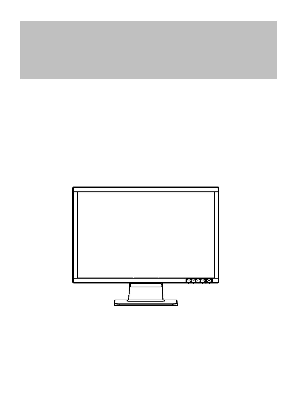
19” LCD Monitor
193FW (+)
THESE DOCUM ENTS ARE FOR REPAIR SERVICE INFO RMAT ION ONLY. EVERY REASONABLE EF FORT
HAS BEEN MADE TO ENSURE THE ACCURACY OF THIS MANUAL; WE CANNOT GUARANTEE THE
ACCURACY OF THI S INFORMATION AFTER THE DATE OF PUBLICATION AND DISCLAIMS RELIABILITY FOR
CHANGES, ERROR S OR O MI S SIO NS.
1
Page 2

AOC 193FW (+)
Ta b le of Content
Revision List………………………………………………………………………………………………………….
1. Monitor Specifications…………………………………………………………………………………………..
2. LCD Monitor Description………………………………………………………………………………………..
3. Operating Instructions…………………………………………………………………………………………..
3.1 General Instructions…………………………………………………………………………………………... 6
3.2 Control Buttons………………………………………………………………………………………………... 6
3.3 Adjusting the Picture………………………………………………………………………………………….. 7
3
4
5
6
4. Input/Output Specification……………………………………………………………………………………...
4.1 Input Signal Connector……………………………………………………………………………………….. 9
4.2 Factory Preset Display Modes……………………………………………………………………………….. 9
4.3 Power Supply Requirem ents ………………………………………………………………………………… 10
4.4 Panel Specification………………………………………………………………………………………….… 10
4.4.1Display Characteristics………………………………………………………………………………… 10
4.4.2Optical Characteristics…………………………………………………………………………………… 11
4.4.3 Parameter Guide Line For CCFL Inverter……………………………………………………………… 11
5. Block Diagram………………………………………………………………………………………………….…
5.1 Monitor Exploded View……………………………………………………………………………………….. 12
5.2 Software Flow Chart…………………………………………………………………………………………... 13
5.3 Electrical Block Diagram……………………………………………………………………………………… 15
5.3.1 Main Board………………………………………………………………………………………………... 15
5.3.2 Inverter/Power Board………………………………………………………….…………………………. 16
6. Schematic……………………………………………………………………………………………………….…
6.1 Main Board…………………………………………………………………………………………………….. 17
6.2 Power Board……………………………………………………………………….………………………….. 24
7. PCB Layout……………………………………………………………………………………………………….
7.1 Main Board…………………………………………………………………………………………………….. 27
9
12
17
27
7.2 Adapter Board………………………………………………………………………….……………………… 28
7.3 Inverter Board ………………………………………………………………………………………………… 28
8. Maintainability…………………………………………………………………………………………………….
8.1 Equipments and Tools Requirement………………………………………………………………………… 29
8.2 Trouble Shooting…………………………………………………………………………………………….… 30
8.2.1 Main Board………………………………………………………………………………………………... 30
8.2.2 Adaptor /Inverter/Board………………………………………………………………………………… 33
8.2.3 Keypad Board…………………………………………………………………………………………….. 34
9. White-Balance, Luminance adjustment ……………………………………………………………………
10. EDID Content…………………………………………………………………………………………………….
11. BOM List……………………………………………………………………………………………………….....
12. Different Parts list………………………………………………………………………………………….
29
35
36
37
181
2
Page 3

AOC 193FW (+)
Revision List
Version Date Revision History TPV Model Name
A00 Jan-16-06
A01
A02
A03 Oct-05-06 Add the sold area model
A04 Oct-25-06 Add the sold area model T95MM2HCWCPUNP
A05
A06 Nov-30-06 Add BOM in item 11 T982KM2HMBUIN
A07 Jan-26-07 Add BOM in item 11 T96MM2NQWCA1N
A08 Jun-05-07 Add BOM in item 11 T95MM2HCWCCGNP
Sep-13-06 Add the sold area model T95MM2HLWCCKNP
Sep-18-06 Add the sold area model T95MM2HMWCUPNP
Nov-22-06 Add TPV Model in item 12 T982KM4HBAE1NP
Initial Release T982KM2HDBAON
T982KM2NKBA1N
T982KM2NKBA1NP
T95MM2HKWCA1FP
3
Page 4
1. Monitor Specifications
Items Specifications
AOC 193FW (+)
Driving system TFT Color LCD
Size 48.0cm(19.0")
LCD Panel
Input
Display Color 16.7M colors
Dot Clock 135MHz
Contrast Ratio 500:1
White Luminance 300cd/m
Max. Resolution 1440 × 900 @60Hz
Plug & Play VESA DDC2BTM
Power Consumption
Pixel pitch 0.285mm(H) x 0.285mm(V)
Viewable angle 150˚ (H) 130˚ (V)
Response time (type) 8 ms for AU p anel
Separate Sync.
15Pin R, G, B Analog signal
Video
H-Frequency 30kHz – 80kHz
V-Frequency 55-75Hz
2
ON Mode<36W
OFF Mode<1W
H/V TTL
24Pin DVI digital signal
Power Source 100~240VAC,47~63Hz
Maximum Screen Size
Environmental
Considerations
Horizontal : 410mm
Vertical: 256mm
Operating Te mp: 5°C to 50°C
Storage Temp: -20°C to 60°C
Operating Humidity: 10% to 85%
4
Page 5
AOC 193FW (+)
For white balance
Keyboard
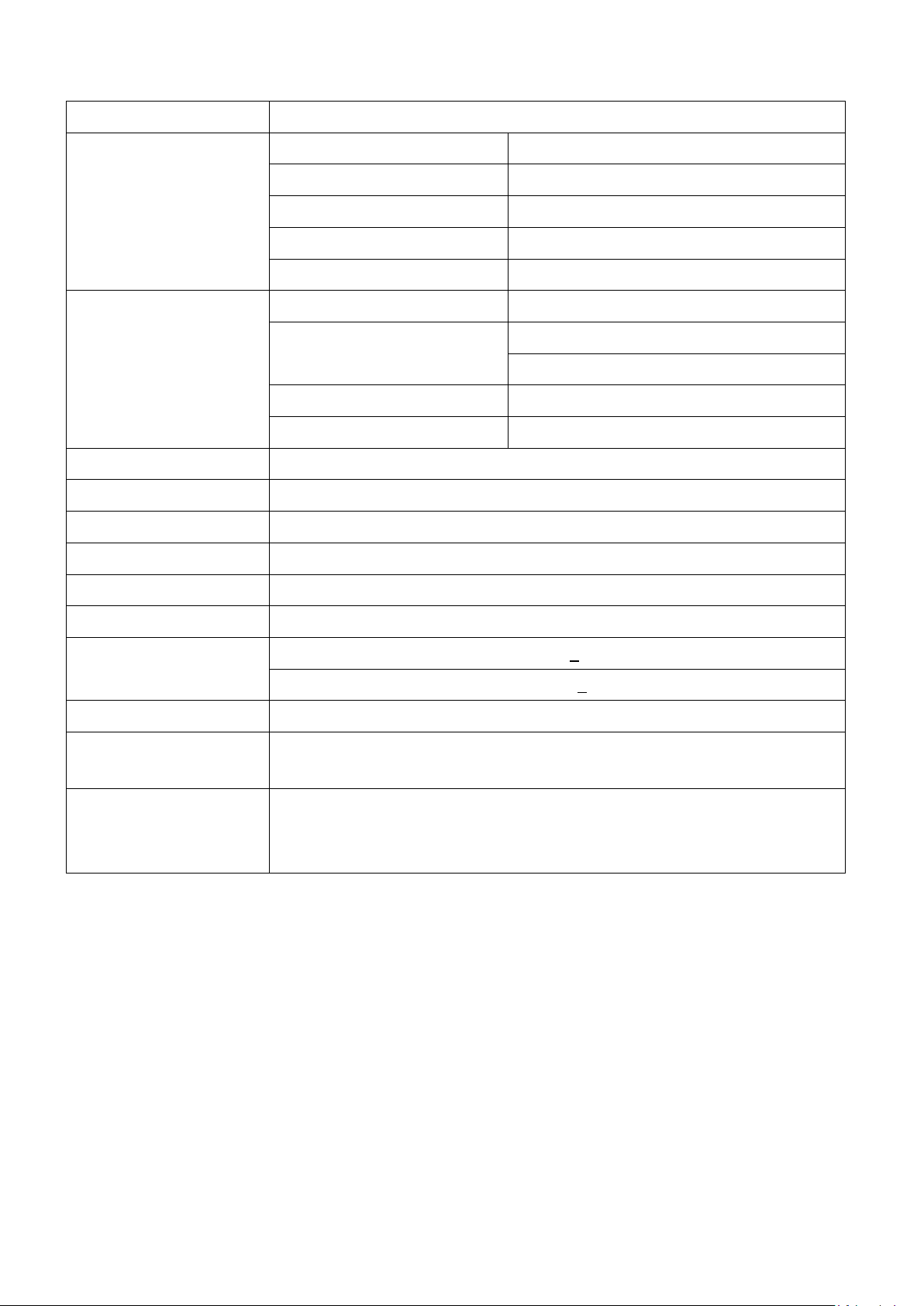
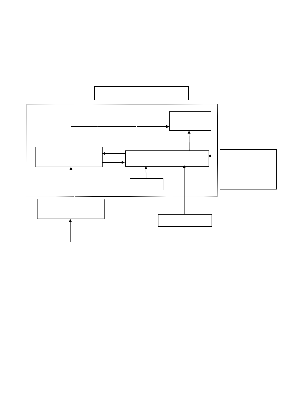
2. LCD Monitor Description
The LCD MONITOR wil l contain a m ain board, an a dapter, an inverter boar d and a keypad board which h ouse the
flat panel control logic, brightness control logic and DDC.
The Inverter board will drive the backlight of panel and the DC-DC conversion.
The Adapter will provide the 12V DC-power to inverter/power board.
Monitor Block Diagram
CCFL Drive.
Flat Panel and
CCFL backlight
Inverter board
Main Board
RS232 Connector
DC-IN
12V
adjustment in factory
mode
Adaptor board
Video signal
AC-IN
100V-240V
HOST Computer
5
Page 6
AOC 193FW (+)
3. Operating Instructions
3.1 General Instructions
Press the power butto n to turn the m onitor on or off. The other co ntrol butto ns are located at front panel of t he
monitor.
By changing these settings, the picture can be adjusted to your personal preferences.
The power cord should be connected.
-
Connect the video cable from the monitor to the video card.
-
Press the power button to turn on the monitor, the power indicator will light up.
-
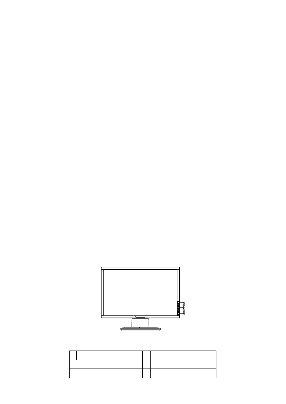
3.2 Control Buttons
- Power Button:
When pressed, the monitor enters the off mode, and the LED turns blank. Press again to restore normal status.
- Contrast:
Adjust contrast or function adjusts.
- Brightness:
Adjust brightness or function adjusts.
- Auto Adjust button / Exit:
When OSD menu is in active status, this button will act as EXIT-KEY (EXIT OSD menu).
1.
2. When OSD menu is in off status, press this button over 2 seconds to activate the Auto Adjustment function.
The Auto Adjustment function is used to set the HPos, VPos, Clock and Focus.
- Power Indicator:
Green — Power On mode.
Red — Off mode.
OSD Lock Function: To lock the OSD, press and hold the MENU button while the monitor is off and then press power button to
turn the monitor on. To un-lock the OSD - press and hold the MENU button while the monitor is off and then pre ss pow er button
to turn the monitor on.
Power Key
1.
MENU/ENTER
3.
Brightness
5.
LED
2.
Contrast
4.
Auto Adjust Key/Exit
6.
6
Page 7
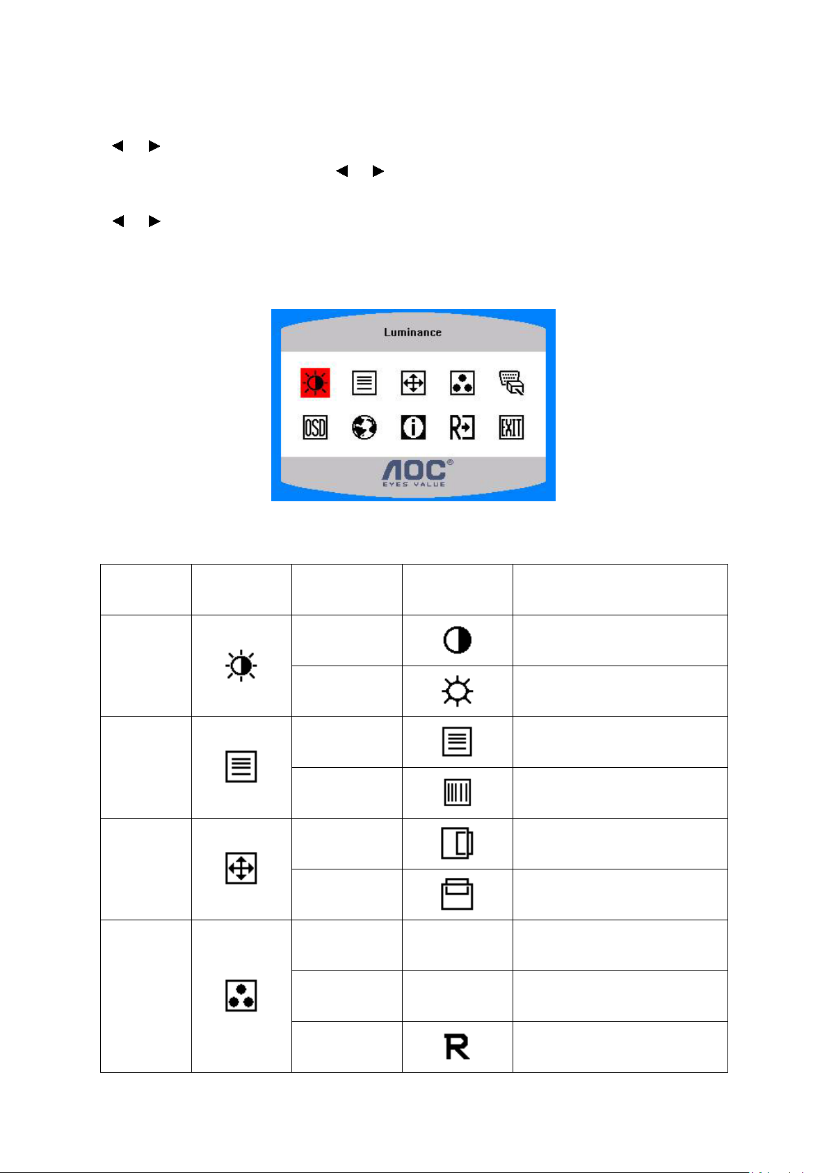
3.3 Adjusting The Picture
Adjustment steps:
1. Press the MENU-button to activate the OSD window.
AOC 193FW (+)
2. Press
it. If the function selected has a sub-menu, press or again to navigate through the sub-menu functions. Once the desired
function is highlighted, press ME NU -button to activate it.
3. Press or to change the settings of the selected function.
4. To exit and save, select the exit function. If you want to adjust any other function, repeat steps 2-3.
or to navigate through the functions. Once the desired f unctio n is high lighted, pr ess the M ENU -button to act ivate
OSD TABLE:
Main Menu
Item
Luminance
Image Setup
Image
Position
Main Menu
Icon
Sub Menu Item Sub Menu Icon Description
Contrast
Contrast from Digital-register.
Brightness
Backlight Adjustment
Adjust Picture Phase to reduce
Focus
Horizontal-Line noise
Adjust picture Clock to reduce
Clock
Vertical-Line noise.
Adjust the horizontal position of
H. Position
the picture.
Adjust the vertical position of the
V. Position
picture.
Recall Warm Color Temperature
Warm N/A
from EEPROM.
Color T emp.
Cool N/A
Recall Cool Color Temperature
User / Red
Red Gain from Digital-register.
from EEPROM.
7
Page 8
AOC 193FW (+)
frequency and input port of current
Input signal
select
OSD Setup
User / Green
User / Blue
Analog
Digital N/A Select the digital signal input
H. Position
V. Position
OSD Timeout
English N/A
Deutsch N/A
N/A Select the analog signal input
Green Gain Digital-register.
Blue Gain from Digital-register.
Adjust the horizontal position of
the OSD.
Adjust the vertical position of the
OSD.
Adjust the OSD timeout.
Set OSD display language to
English.
Set OSD display language to
German.
Language
Information
Reset
Français N/A
Español N/A
Italiano N/A
简体中文 N/A
Information N/A
Yes N/A
No N/A
Set OSD display language to
French.
Set OSD display language to
Spain.
Set OSD display language to
Italian.
Set OSD display language to
Simplified Chinese.
Show the resolution, H/V
input timing.
Clear each old status of
Auto-configuration and set the
color temperature to Cool.
Do not execute reset, return to
main menu.
Exit
N/A N/A Exit OSD
8
Page 9
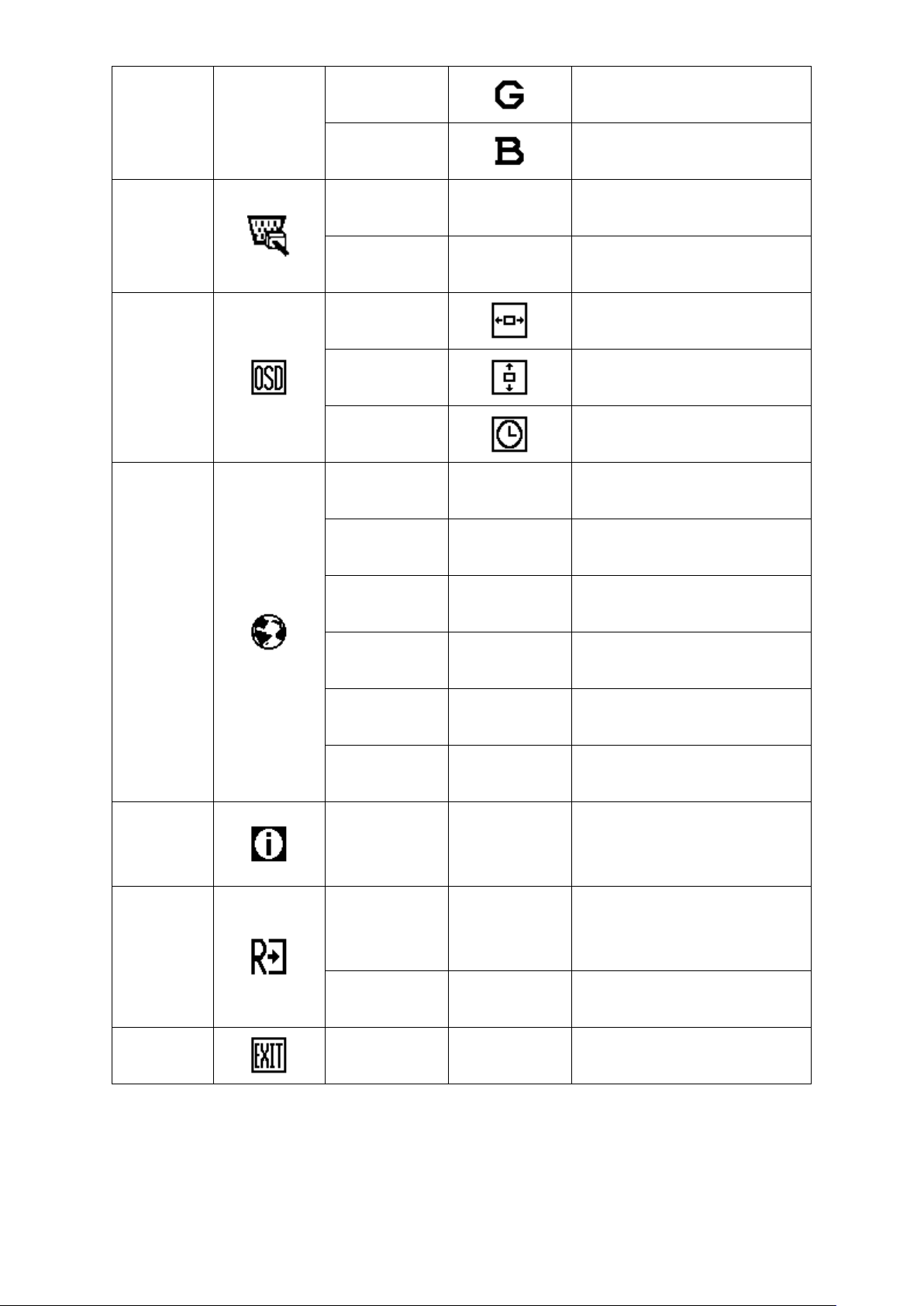
4. Input/Output Specification
1
5
61011
15
4.1 Input Signal Connector
Analog connector
Pin No. Description Pin No. Description
AOC 193FW (+)
1.
2.
3.
4.
5.
6.
7.
8.
DVI-D connector
Red Video
Green Video
Blue Video
Ground
Ground
Red Ground
Green Ground
Blue Ground
VGA connector layout
9.
10.
11.
12.
13.
14.
15.
Detect Cable
Ground
DDC-Serial Data
H-Sync
V-Sync
DDC-Serial Clock
+5V
Pin No.
1.
2.
Description
TMDS data 2-
TMDS data 2+
Pin No.
13.
14.
Description
TMDS data 3+
+5V Power
3. TMDS data 2/4 Shield 15. GND
4.
5.
6. DDC Clock 18.
TMDS data 4-
TMDS data 4+
16. Hot Plug Detect
17.
TMDS data 0-
TMDS data 0+
7. DDC Data 19. TMDS data 0/5 Shield
8. Analog Vertical Sync 20.
9.
10.
TMDS data 1-
TMDS data 1+
21.
22. TMDS Clo c k Shi eld
TMDS data 5-
TMDS data 5+
11. TMDS data 1/3 Shield 23. TMDS Clock +
12.
TMDS data 3-
24.
TMDS Clock -
24 - Pin Color Dis pl a y Signal Cable
9
Page 10
4.2 Factory Preset Display Modes:
Dos-mode
720 × 400
31.47kHz
70.0Hz
640 × 480
31.47kHz
60.0Hz
640 × 480
37.50kHz
75.0Hz
800 × 600
37.879kHz
60.0Hz
800 × 600
46.875kHz
75.0Hz
1024 × 768
48.363kHz
60.0Hz
1024 × 768
56.476kHz
70.0Hz
1024 × 768
60.021kHz
75.0Hz
1280 × 1024
64.000kHz
60.0Hz
1280 × 1024
80.000kHz
75.0Hz
WXGA
1440 × 900
55.935kHz
59.8Hz
AOC 193FW (+)
Standard
VGA
SVGA
XGA
SXGA
Resolution
4.3 Power Supply Requirements
A/C Line voltage range 100 V ~ 240 V
Horizontal
Frequency
Vertical
Frequency
A/C Line frequency range
Current 1.5A max at 100V; 0.8A max at 240 V
Peak surge current < 55A peak at 240 VAC and cold starting
Leakage current < 3.5mA
Power line surge
DC output Voltage 5VDC ± 5%; 12VDC± 5%
CURRENT 1.5Amp (5V) ;2 Amp (12V)
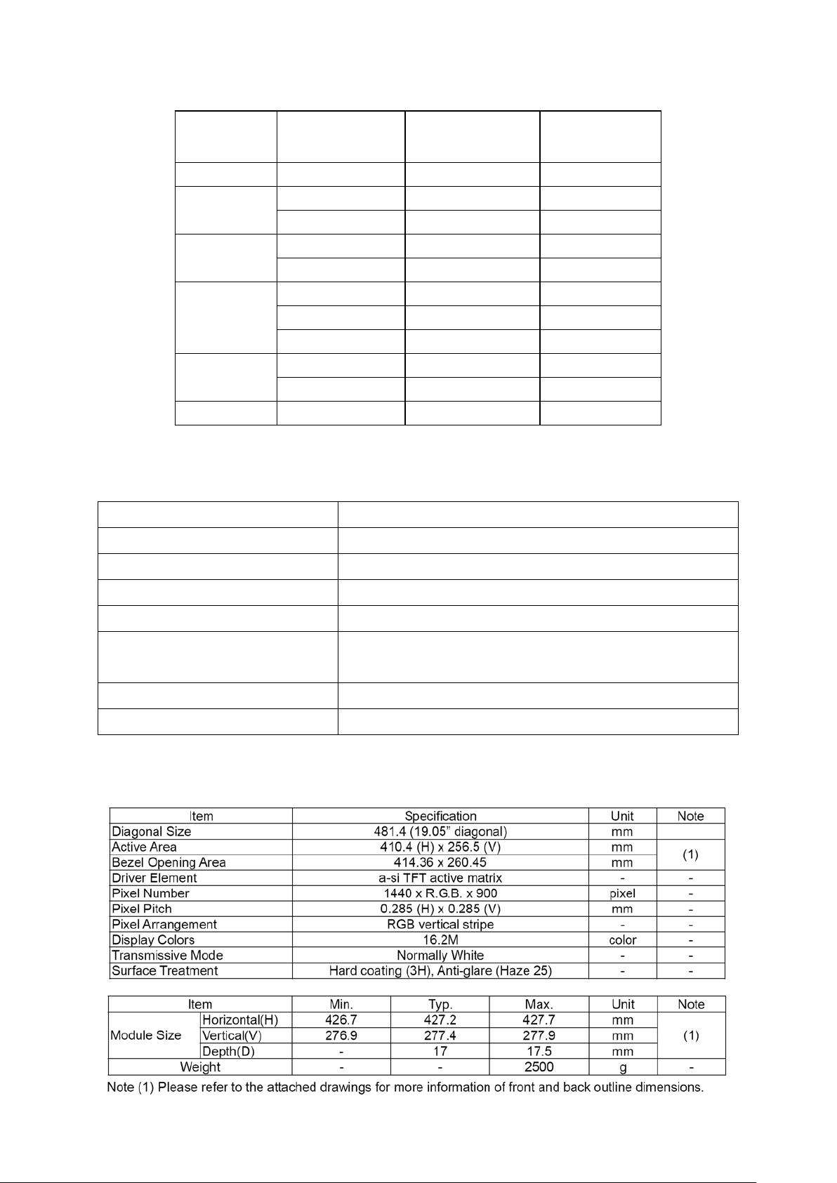
4.4 Panel Specification
4.4.1 Display Characteristics
50 ± 3Hz, 60 ± 3Hz
No advance effects (no loss of information or defect)
with a maximum of 1 half-wave missing per second
10
Page 11
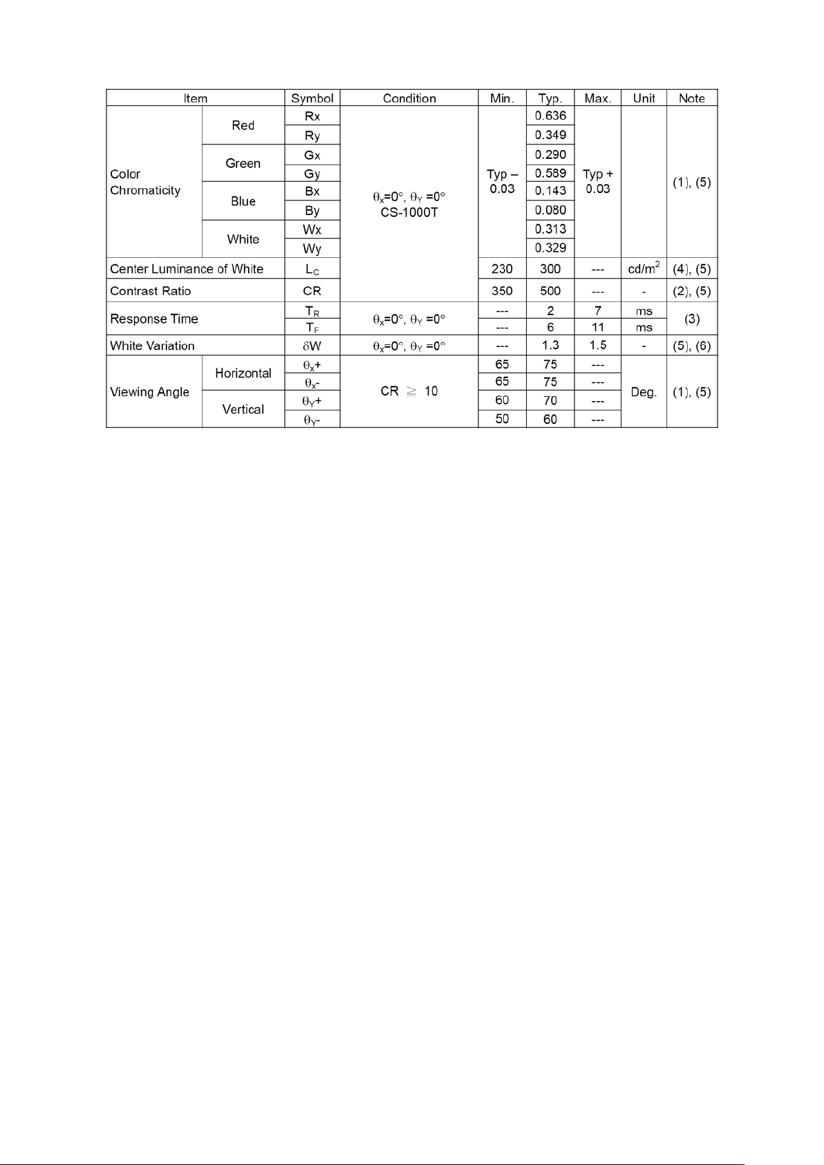
4.4.2 Optical Characteristics
AOC 193FW (+)
11
Page 12
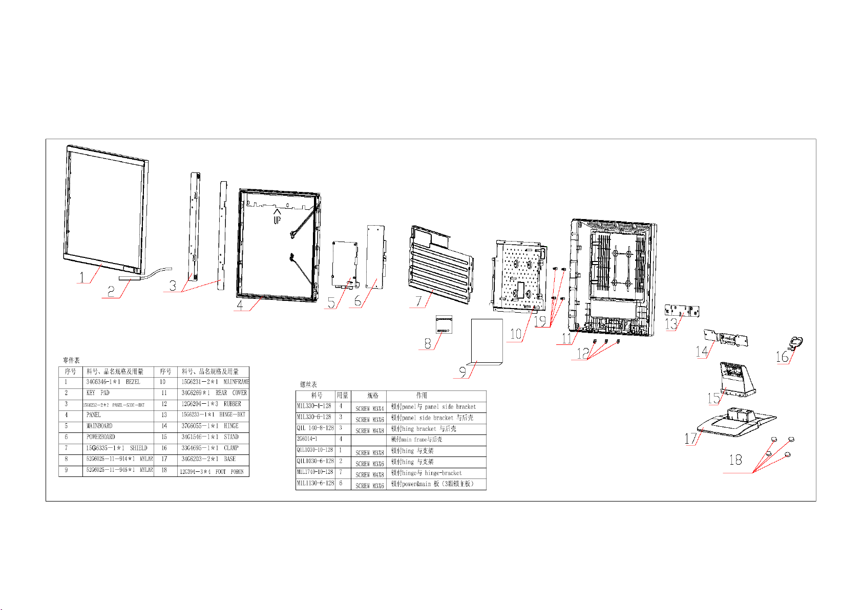
5. Block Diagram
5.1 Monitor Exploded View
AOC 193FW (+)
12
Page 13
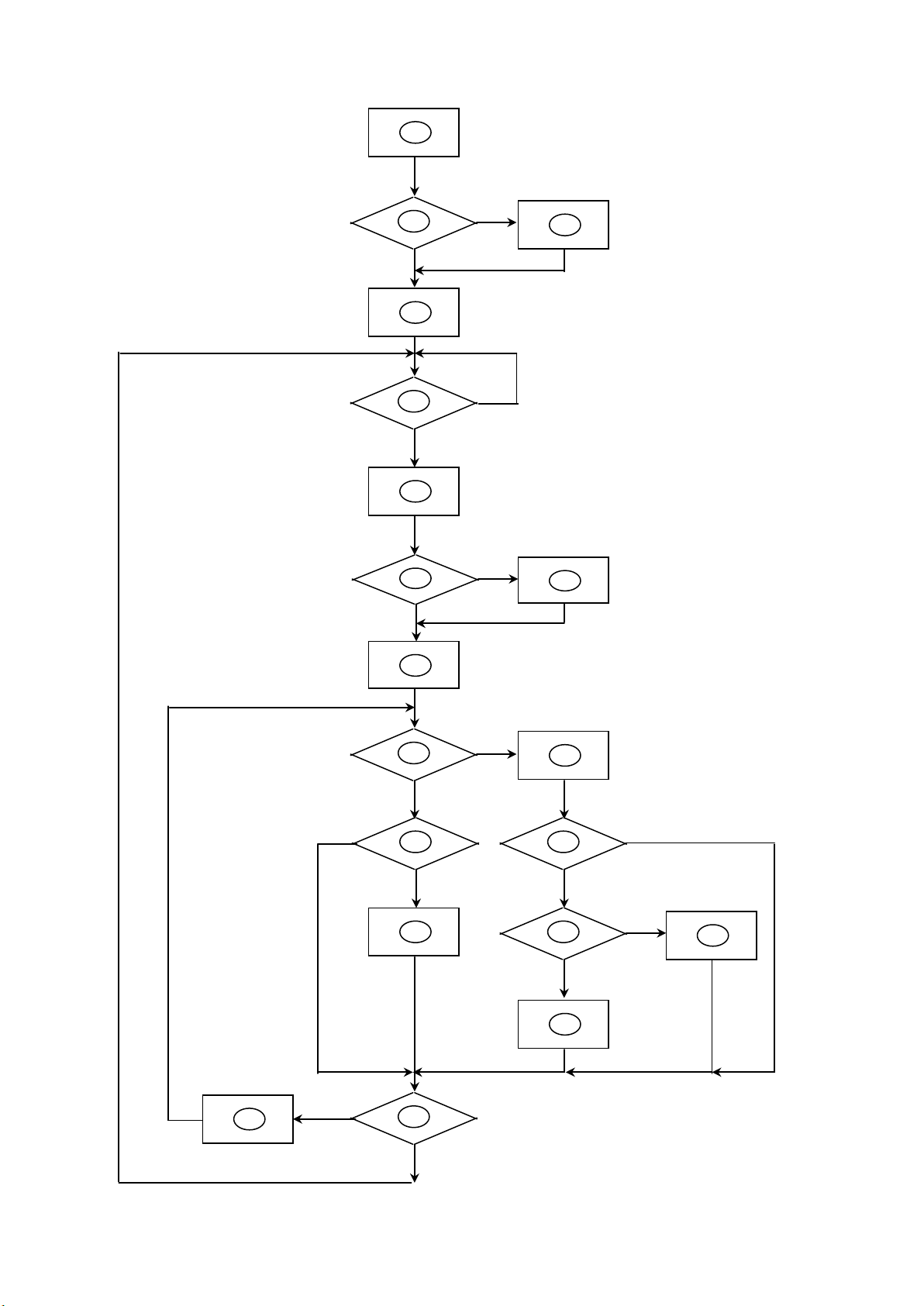
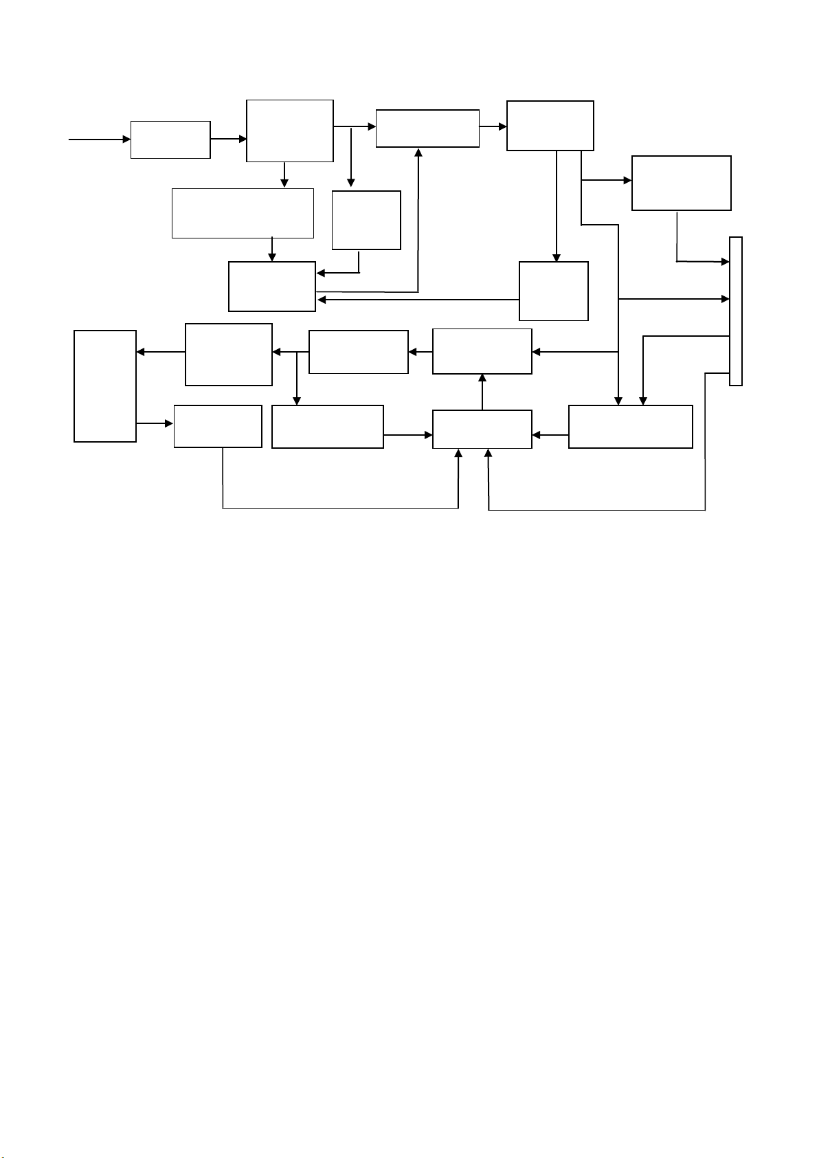
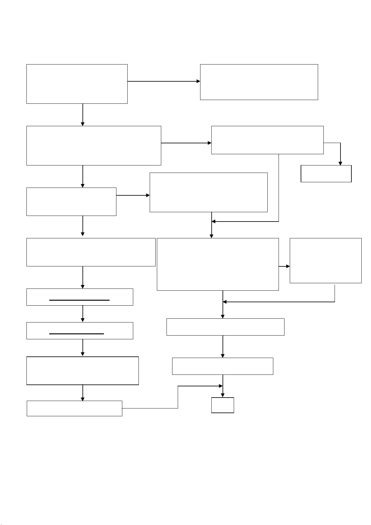
5.2 Software Flow Chart
1
2
N
Y 5 Y
N
10
Y
N
12
Y
N
7 N 6 4 3
9
14
11
13
Y
N
15
Y
N
16
17
19
Y
N
18
AOC 193FW (+)
13
Page 14

AOC 193FW (+)
standby mode after the
1) MCU initializes.
2) Is the EPROM blank?
3) Program the EPROM by default values.
4) Get the PWM value of brightness from EPROM.
5) Is the power key pressed?
6) Clear all global flags.
7) Are the AUTO and SELECT keys pressed?
8) Enter factory mode.
9) Save the power key status into EPROM.
Turn on the LED and set it to green color.
Scalar initializes.
10) In standby mode?
11) Update the lifetime of back light.
12) Check the analog port, are there any signals coming?
13) Does the scalar send out an interrupt request?
14) Wake up the scalar.
15) Are there any signals coming from analog port?
16) Display "No connection Check Signal Cable" message. And go into
messages disappear.
17) Program the scalar to be able to show the coming mode.
18) Process the OSD display.
19) Read the keyboard. Is the power key pressed?
14
Page 15
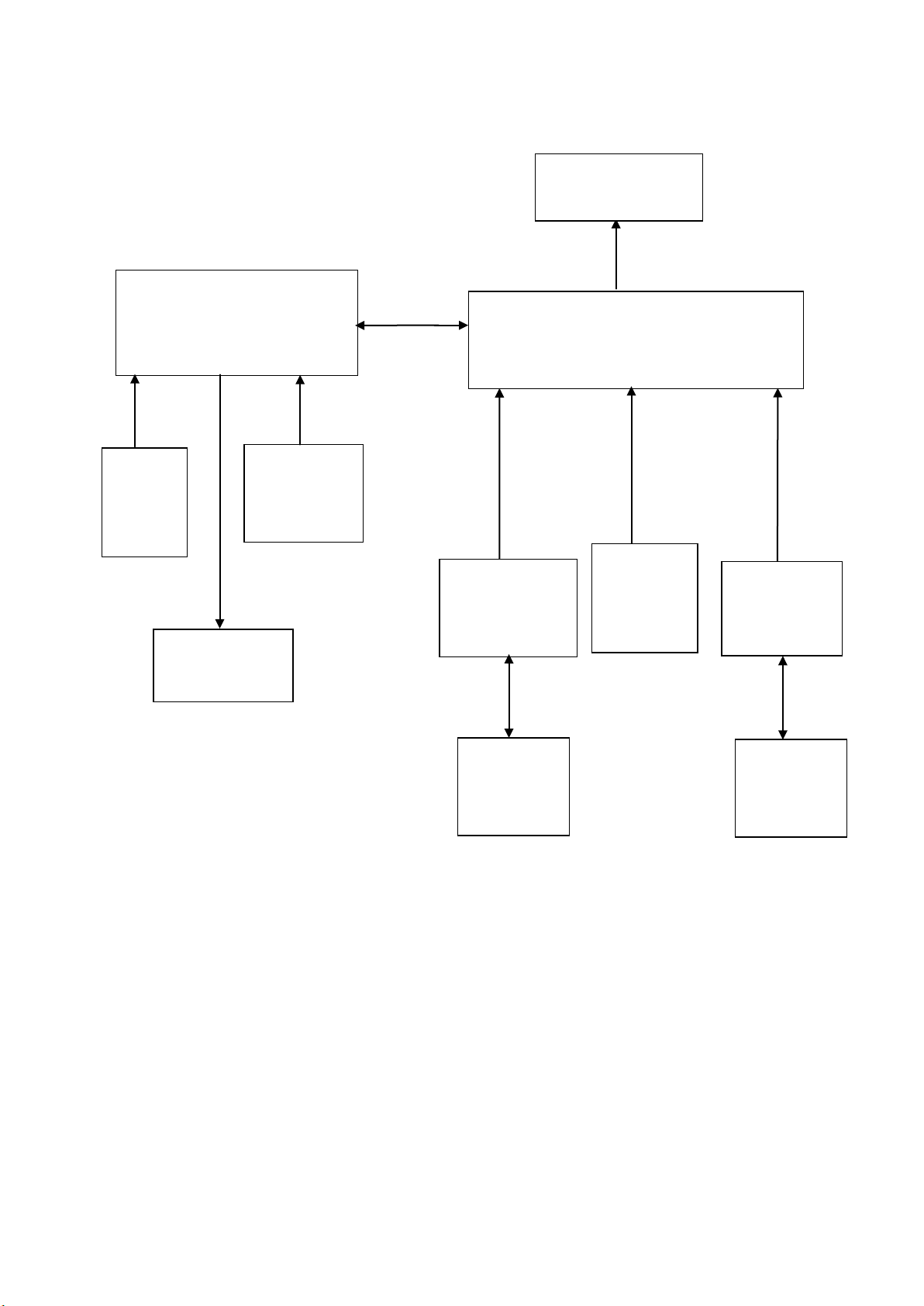
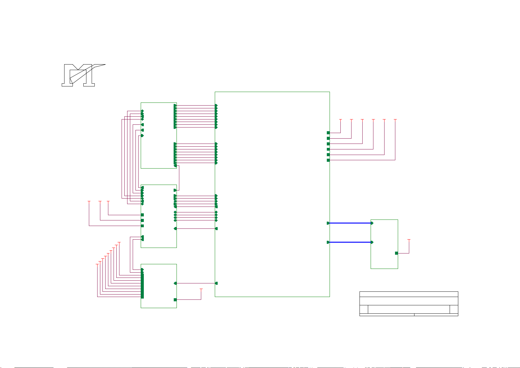
5.3 Electrical Block Diagram
DB15_SCL
SCL
5.3.1 Main Board
AOC 193FW (+)
LCD Interface
(CN503)
MTV512 MV 44PIN-PLCC
Crystal
X601
24Mhz
MCU
(U601)
Key Board
EPR_SDA
EPR_SCL
EEPROM
AT24C16N
(U602)
TSU56AK-LF
(Include ADC, OSD)
(U401)
RGB
CLK+
CLK-
DVI
Connector
(CN302)
H sync
V sync
RGB
Connector
(CN301)
Crystal
D-Sub
X601
14.318Mhz
CN602
DB15_SDA,
SDA,
EEPROM
M24C02
(U301)
EEPROM
M24C02
(U302)
15
Page 16
5.3.2 Inverter/Power Board
PWM
Feed
AC input
PWM
Feedback
Circuit
OSC and
DC Convert
Circuit
Over Voltage
Protect
ON/OFF
DIM
Protect
EMI filter
Bridge
Rectifier
and Filter
Transformer
Rectifier
diodes
AOC 193FW (+)
Lamp
Start Circuit: R903、
R904
Control IC
Output
Circuit
Over
Voltage
MOSFET
PWM
Control IC
back
circuit
DC-to-DC IC
12V
ON/OFF Control
CN201
5V
16
Page 17

Page 18
6. Schematic
VAA3
VCC12V
B4
2.POW ER
onPanel_5V/3.3V
onBACKLITE
AdjBACKLITE
VCC3.3
VCC1.8
VAA1
VAA2
VAA3
VAA4
VCC5V
VCC12V
VLCD
VCPU
VLCD
VAA4VAA3
VCC12V
B3
6.MCU
onBACKLITE
onPANEL_5V/3.3V
SDA
INT
CSZ
DDC_DAT
ST_D ET1
SCL
HWRESET
DDC_CLK
Volume
VCC5V
VCC12V
VCPU
RXD
TXD
AD0
AD1
AD2
AD3
DDC_WPDVI_DET
DDCCI_SEL
VCC5V
VAA2
VAA4
VCPU
B5
5.PANEL INTERFA CE
VLCD
PB[0..9]
PA[0..9]
VCC3.3
B1
3.INPUT
RIN
GIN
BIN
VSYNC
GNDR
GNDG
GNDB
ST_D ET1 HSYNC
SOGDDC_CLK
DDC_DAT
R+
RG-
G+
B+
B-
CLK+
CLK-
TXD
RXD
DDC_WP
DVI_DET
DDCCI_SEL
VCC5V
PA[0..9]
PB[0..9]
VCC1.8
B2
4.SCALER
RIN
GIN
SOG
BIN
GNDR
GNDG
GNDB
HSYNC
VSYNC
R+
R-
G-
G+
B+
BCLK+
CLK-
CSZ
SCL
SDA
HWRESET
INT
Volume
AdjBACKLITE
PA[0..9]
PB[0..9]
VCC1.8
VCC3.3
VAA1
VAA2
VAA3
VAA4
AD0
AD1
AD2
AD3
VAA1
TOP B
TSU56AK FOR MYSON512 SWITCH
B
1 6Wednesday , Oc t ober 06, 2004
Title
Size Docum ent N um ber Rev
Date: Sheet
of
VAA1
VCPU
VLCD
VCC1.8
VCC3.3
VAA2
TSU56AK SCHEMATIC
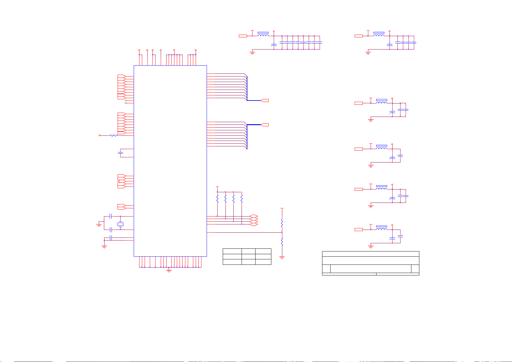
6.1 Main Board
AOC 193FW (+)
18
Page 19
AOC 193FW (+)
R214
NC
FB201
NC
TO-263
VCPU 6
+
C215
47uF/16V
DIM
R201 4.7K£[ 1/ 16W
R208
10K£[ 1/16W
FB202
600 OHM
R212 4.7K£[ 1/ 16W
VCC1.8 4
Q204
PMBS3904
CE
B
VCC12V
VCPU
C207
0.1uF
C214
0.1uF
C201
0.1uF
VLCD 5
Q202
PMBS3904
CE
B
+
C208
10uF/16V
onPanel_5V/3.3V6
VCC12V
D201 SS14
C203
0.1uF
VCC5V+
C
B E
C216
0.1uF
C212
0.1uF
VCC3.3 4
VLCD
VCC3.3
VCC12V
VCC3.3
R206
10K£[ 1/16W
R210
NC
GND
+
C218
47uF/25V
C206
1uF/25V
VCC5V
U202
AIC1084-33M
3
1
2
VIN
ADJ
VOUT
GND
R204
10K£[ 1/16W
VAA4 4
R209
0£[ 1/16W
H1
SCREW3.2RM
1
2
3
4
5
6
7
8
9
123
4
5
678
9
GND
+
C202
220uF/25V
U201
AZ1117D-1.8
3 2
1
VI VO
GND
VCC5V+
+
C204
220uF/25V
VAA3 4
Brightness
R202
10K£[ 1/16W
GND
R203
1K£[ 1/16W
VCC5V
C210
0.1uF
VCC5V
VCC5V+
C219
0.1uF/16V
POWER B
TSU56AK FOR MYSON512 SWICH
B
2 6Wednesday , Oc t ober 06, 2004
Title
Size Docum ent N um ber Rev
Date: Sheet
of
H4
SCREW3.2RM
1
2
3
4
5
6
7
8
9
123
4
5
678
9
C
B E
VAA2 4
VCC12V
2004/09/05 ADD
TOUCH PANEL
POWER
VAA1
VAA4
+
C211
47uF/16V
Q201
PMBS3904
CE
B
C217
0.1uF
VCC5V
ON_OFFGND
VCC5V
C205
0.1uF
Q203
AO3401
PITCH 2.0
CN202
CONN
1
2
R211
10K£[ 1/16W
SOT-252
VCC5V
VCPU
R205 4.7K£[ 1/ 16W
D202
GS1D
R207 4.7K£[ 1/ 16W
VAA1 4
VCC5V
CN201
CONN
2
4
6
8
10
12
1
3
5
7
9
11
VCC1.8
VCC12V
H2
SCREW3.2RM
1
2
3
4
5
6
7
8
9
123
4
5
678
9
GND
VCC12V 6
VAA2
VCC5V
VCC5V
VCC5V 3,4,6
VAA3
GND
R213
NC
R215
51K£[ 1/16W
onBACKLITE 6
AdjBACKLITE4
19
Page 20
AOC 193FW (+)
C310 0.047uF
R350 10£[ 1/16W
PC5V C302
NC
SOG 4
C323
0.1uF
4/2/2004-Add W/P control by MCU
R340
0£[ 1/16W
D305
BAV70
3
1
2
GIN 4
D326
BAV70
3
1
2
C309 0.047uF
DDC_CLK6
VGA_CON
D322
TZMC5V6-GS08 NC
R334
NC
C315
0.1uF
FB302 0£[ 1/16W
4/2/2004-Add R329,R330
Q301
PMBS3904
CE
B
DDCCI_SEL 6
D309
BAV99
3
1
2
R338
10K£[ 1/16W
D319
TZMC5V6-GS08
VCC5V
R306 68£[ 1/ 16W
R327
75£[ 1/16W
C303
NC
4/2/2004-Add D324 Solution
D320
TZMC5V6-GS08
C306 0.047uF
BIN 4
R+ 4
R343 10£[ 1/16W
R345 10£[ 1/16W
R310 1K£[ 1/ 16W
D303
BAV99
3
1
2
R330NC
GNDG 4
DVIDDC_5V
R335
4.7K£[ 1/16W
operating
voltage-2.5v-5.5v
VCC5V
R316 100£[ 1/ 1 6W
R333
NC
R301 33£[ 1/ 16W
VCC5V
R346 10£[ 1/16W
G+ 4
operating
voltage-2.5v-5.5v
U302
M24C02WMN6
1
2
3
45
6
7
8
A0
A1
A2
GNDSDA
SCL
WP
VCC
PC5V
D301
BAV99
3
1
2
C324
0.1uF
R329NC
C307 0.001uF
R349 10£[ 1/16W
D323
TZMC5V6-GS08 NC
R344 10£[ 1/16W
R319 100£[ 1/ 1 6W
ST_D ET1 6
2004/09/05
ADD ESD
Solution
DVI_HPD
R320 100£[ 1/ 1 6W
C318
0.1uF
VCC5V
CN301
DB15
1
6
2
7
3
8
4
9
5
11
12
13
14
15
10
16
17
D317
TZMC5V6-GS08
C311
47pF
R323
10K£[ 1/16W
D310
BAV99
3
1
2
D321
TZMC5V6-GS08
DVI5V
R326
75£[ 1/16W
R309 100£[ 1/ 1 6W
HSYNC 4
VCC5V
R339 4.7K£[ 1/16W
R314
2.2K£[ 1/16W
R342 NC
VSYNC 4
TXD 6
DSUBDDC_5V
CLK_DDC2
C304 0.047uF
D314
LL5232B 5.6V 5%
C319
0.1uF
R- 4
GNDB 4
C305 0.047uF
U303
74VHC4053
12
11
2
1
5
4
6
13
10
9
14
15
3
7
8
16
0A
SA
0B
1B
0C
ZC
INH
1A
SB
SC
ZA
ZB
1C
VEE
GND
VCC
D316
LL5232B 5.6V 5%
C320
0.1uF
R312 100£[ 1/ 1 6W
VCC5V
D318
TZMC5V6-GS08
DDC_DAT 6
DSUBDDC_5V
D324
BAV99/NC
3
1
2
FB304 430 OHM
C325
0.1uF
R336 4.7K£[ 1/16W
CLK+ 4
RIN 4
DVI5V
D315
LL5232B 5.6V 5%
D307
BAV99
3
1
2
R313
2.2K£[ 1/16W
INPUT B
TSU56AK FOR MYSON512 SWITCH
C
3 6Wednesday , Oct ober 06, 2004
Title
Size Docum ent N um ber Rev
Date: Sheet
of
DVIDDC_5V
C301
NC
VCC5V
C322
0.1uF
DDC_WP 6
C314
0.1uF
DDC_CLK 6
D308
BAV99
3
1
2
B+ 4
R303 33£[ 1/ 16W
CLK_DDC
GNDR 4
B- 4
VCC5V
R321
10K£[ 1/16W
R325
75£[ 1/16W
CLK- 4
C313
0.1uF
DAT_DDC
D313
BAV99
3
1
2
R348 10£[ 1/16W
FB303 0£[ 1/16W
VCC5V
CN302
JACK NC
1
2
3
4
5
6
7
8
25
28
9
10
11
12
13
14
15
16
26
29
17
18
19
20
21
22
23
24
27
31
32
DAT2 -
DAT2 +
2/4shield
DAT4 -
DAT4 +
DDC SCL
DDC SDA
VSYNC
R
HSYNC
DAT1 -
DAT1 +
1/3shield
DAT3 -
DAT3 +
+5V
SYNC GND
HPD
G
RGB GND
DAT0 -
DAT0 +
0/5shield
DAT5 -
DAT5 +
clk shield
clk+
clk-
B
31
32
C321
0.1uF
D304
BAV70
3
1
2
D312
BAV99
3
1
2
R315 100£[ 1/ 1 6W
DDC_DAT6
G- 4
HSI
R318
10K£[ 1/16W
R347 10£[ 1/16W
RXD 6
R304 470£[ 1/ 1 6W
R317
10K£[ 1/16W
2004/08/19 ADD
U301
M24C02WMN6
1
2
3
45
6
7
8
A0
A1
A2
GNDSDA
SCL
WP
VCC
D311
BAV99
3
1
2
R305 68£[ 1/ 16W
R324
10K£[ 1/16W
R302 33£[ 1/ 16W
DAT_DDC2
R337 4.7K£[ 1/ 16W
C312
220pF
C308 0.047uF
8/9/2004-Add DVI
CABLE Detect
R341 NC
FB301 0£[ 1/16W
R331
10K£[ 1/16W
DVI_DET 6
C316
0.1uF
VSI
D302
BAV99
3
1
2
R311 1K£[ 1/ 16W
C317
0.1uF
D325
MLL5232B 5.6V
R307 68£[ 1/ 16W
8/9/2004-Add DDC/CI
Solution
R332 1K£[ 1/16W
R308
10K£[ 1/16W
D306
BAV99
3
1
2
20
Page 21
VCC5V
R404
10K£[ 1/16W
BIN3
VDPLL
PB8
PA6
R402
100£[ 1/16W
VAA4
R401
VAA3
C426
0.1uF
CSZ6
HSYNC3
PA9
PB5
C417
0.1uF
B+3
4.7K
VCC1.8
VCC3.3
PB1
PB2
GNDR3
B-3
FB403
600 OHM
FB404
600 OHM
PB[0..9] 5
VAA22
NC
R407
10K£[ 1/16W
C423
0.1uF
R+3
VPO
VAD
VCC3.32
PA5
PA8
C404 0.1uF
GIN3
4.7K
AD2 6
VAA42
CLK-3
+
C405
10uF/16V
PB9
+
C424
10uF/16V
C421
0.1uF
R401
NC
3-WIRE
VDPLL
FB402
600 OHM
VAD
VPLL
PB6
FB405
600 OHM
RIN3
PA2
C416
0.1uF
VCC1.82
AD0 6
C428
0.1uF
AdjBACKLITE2
PB7
C418
0.1uF
VAA2
C410
0.1uF
HWRESET6
PA1
VAA1
VDVI
VPO
+
C414
10uF/16V
Volume6
INT6
VDVI
PB4
C406
0.1uF
C408
0.1uF
PA0
VAA32
VPLL
C401
0.1uF
SDA6
PA4
G+3
PB3
AD1 6
+
C419
10uF/16V
AD3 6
C409
0.1uF
PA7
VDD
PA[0..9] 5
CLK+3
VAA12
FB401
600 OHM
GNDG3
PA3
C402 22pF
C413
0.1uF
VDD
C403 22pF
C415
0.1uF
PB0
C411
0.1uF
Direct Bus
X401
14.318MHz
SCL6
+
C427
10uF/16V
C420
0.1uF
R405
10K£[ 1/16W
PA[0..9]
C425
0.1uF
VDVI
R403 390£[ 1/16W
U401
TSU56AK
63
60
61
58
62
59
57
37
38
40
41
43
44
46
47
49
50
52
66
67
69
70
71
32
72
73
74
107
55
35
45
3
51
11
21
84
94
104
114
126
18
87
97
117
39
56
36
2
54
42
10
20
85
95
115
127
19
86
96
105
116
33
34
108
109
110
111
112
113
118
119
120
121
122
123
124
125
128
1
29
28
30
31
53
65
64
48
106
103
102
68
77
78
6
RIN0
GIN0
SOGIN0
BIN0
RIN0M
GIN0M
BIN0M
HSYNC0
VSYNC 0
R+
RG+
GB+
BCK+
CKRE XT
REFP
REFM
CSZ
SDA
SCL
HWRESETZ
INT
PWM0
PWM1
LVACKM
AVDD
AVDD_MPLL
AVDD_DVI
BYPASS
AVDD_DVI
VDDP
VDDP
VDDP
VDDP
VDDP
VDDP
VDDP
VDDC
VDDC
VDDC
VDDC
AVSS_DVI
AVSS
AVSS_MPLL
AVSS_LPLL
AVSS_PLL
AVSS_DVI
GNDP
GNDP
GNDP
GNDP
GNDP
GNDP
GNDC
GNDC
GNDC
GNDP
GNDC
XIN
XOU T
LVA2P
LVA2M
LVA1P
LVA1M
LVA0P
LVA0M
NC/LVB3P
NC/LVB3M
NC/LVBCKP
NC/LVBCKM
NC/LVB2P
NC/LVB2M
NC/LVB1P
NC/LVB1M
NC/LVB0P
NC/LVB0M
DDC1_CLK/GPO8
DDC1_DAT/GPO7
ADO/NC
AD3/NC
AVDD_PLL
AVDD
AVSS
AVSS_DVI
LVACKP
LVA3M
LVA3P
AVSS
AD1/NC
AD2/NC
BUS TYPE/N C
R402
VCC3.3
C407
0.1uF
C412
0.1uF
SOG3
R-3
SCALER B
TSU56AK FOR MYSON512 SWITCH
B
4 6Wednesday , Oc t ober 06, 2004
Title
Size Docum ent N um ber Rev
Date: Sheet
of
PB[0..9]
FB406
600 OHM
VSYNC3
+
C422
10uF/16V
GNDB3
NC
R406
10K£[ 1/16W
G-3
AOC 193FW (+)
21
Page 22
AOC 193FW (+)
RXEC-
LVBCKP
PB3
PA4
LVB1M
PB5
LVA1P
LVBCKM
LVB3P
PA5
LVBCKP
LVACKP
LVA1M
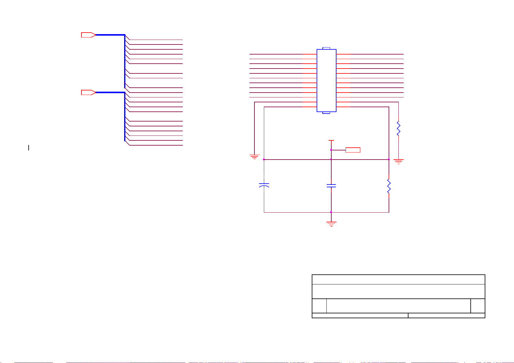
VLCD 2
PB1
LVA0M
LVA3P
C510
0.1uF
RXE2+
RXOC-
PB2
PB4
LVA3M
CN503
CONN
2
4
6
8
10
12
14
16
18
20
22
24
1
3
5
7
9
11
13
15
17
19
21
23
RXOC+
RXE1+
RXO1-
LVACKM
RXE0-
PB7
PA3
RXE1-
R502
0£[ 1/ 16W
LVB2M
VLCD
RXO0-
LVA2M
LVA3M
LVB0P
RXO0+LVACKM
RXO1+
LVB1P
RXE3+
LVA1P
LVA2P
PA[0..9]
PA6
LVB0M
RXE3-
PB0
LVB3M
PB6
LVB1P
RXE0+
RXE2-
PA9
PANEL INTERF ACE B
TSU56AK FOR MY SON512 SWI TCH
A
5 6Wednes day , Oc t ober 06, 2004
Title
Size Doc um ent N um ber Rev
Date: Sheet
of
R503
2.2K£[ 1/ 16W
+
C509
22uF/16V
LVA1M
PA2
LVA0M
PA7
PB[0..9]
LVA0P
LVA3P
LVB0M
LVA2P
PB9
LVBCKM
LVB3PLVB3M
PB[0..9]4
PA8
RXO3+
LVB2P
RXO3-
PA1
PA[0..9]4
PA0
LVB1M
RXO2-
RXEC+
PB8
LVB0P
LVA0P
LVACKP
LVB2P
LVB2M
RXO2+
LVA2M
22
Page 23
X601
24MHz
R601
10K£[ 1/16W
R622 470£[ 1/16W
DDC_CLK 3
R611 220£[ 1/16W
INT4
POWER
R652 10K£[ 1/16W
R638 NC
OUT-R-
RN602
10K£[ 1/16W
1
2
3
4
8
7
6
5
R625 10K£[ 1/16W
DVI_DET 3
RN601
10K£[ 1/16W
1
2
3
4
8
7
6
5
C617
100pF
Q605
PMBS3904
CE
B
ENTER
OUT-R-
U603 MAX810STR (NC)
1
2
3
GND
RST
VCC
R604 10K£[ 1/16W
VCC12V 2
+
C603
10uF/16V
OUT-L-
LED_G
SDA 4
OUT-R+
R618
120£[ 1/16W
R607
10K£[ 1/16W
R624 470£[ 1/ 16W
AD3 4
I/O
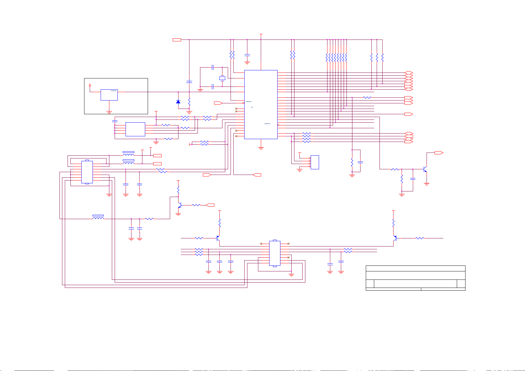
U601
MYSON512
35
21
20
10
14
15
16
2
3
4
5
6
7
8
9
43
42
41
40
39
38
37
36
24
25
26
27
28
29
30
31
19
18
32
33
13
11
22 44
12
17
NC
XTAL 1
XTAL 2
RESET
INT0/P3.2
INT1/P3.3
T0/P3.4
P5.0
P5.1
P5.2
P5.3
P5.4
P5.5
P5.6
P5.7
P1.0
P1.1
P1.2
P1.3
P1.4
P1.5
P1.6
P1.7
P6.0
P6.1
P6.2
P6.3
P6.4
P6.5
P6.6
P6.7
P7.7
P7.6/CLKO
VSYNC
ALE/P
P3.1/TXD
P3.0/RXD
VSS VCC
NC
T1/P3.5
R605 10K£[ 1/16W
FB603
600 OHM
C602 22pF
Mute
FB602 600 OHM
R603
10K£[ 1/16W
Q604
PMBS3904
VCC12V
AUTO
C619
0.1uF/16V
C601
0.1uF
R651
10K£[ 1/16W
C608
0.001uF
C606
0.001uF
VCC5V
OUT-R+
VCPU
R645
nc
VCC5V
2004/08/19 MODIFY
Standby
C609
0.001uF
R619
4.7K£[ 1/ 16W
RIGHT
VCC5V 2,3,4
DDC_WP 3
U602
AT24C16N-10SC-2.7
1
2
3
4 5
6
7
8
A0
A1
A2
GND SDA
SCL
WP
VCC
R646
nc
AD1 4
VCPU
LED_GRN
R609 100£[ 1/16W
CN601
CONN
2
4
6
8
10
12
14
1
3
5
7
9
11
13
FB601 600 OHM
C607
0.001uF
Q601
PMBS3906
C E
B
R614 10K£[ 1/16W
HWRESET 4
RXD 3
CN602
CON16A
2
4
6
8
10
12
14
16
1
3
5
7
9
11
13
15
LEFT
R623 470£[ 1/16W
R641 4.7K£[ 1/ 16W
CSZ 4
R610 220£[ 1/16W
D601
LL4148-GS08
OUT-L+
R644
10K£[ 1/16W
R636 100£[ 1/16W
POWER
Reset
Circuit
R635 NC
R616
4.7K£[ 1/ 16W
R606
10K£[ 1/16W
VCPU
R617
120£[ 1/16W
R626 10K 1/16W
VCPU2
VCC5V
LED_ORANGE
CN603
NC
1
2
3
4
1
2
3
4
Canel R640 R642
ENTER
R647
22K£[ 1/16W
AD2 4
C612
0.1uF
R613
10K£[ 1/16W
ST_D ET13
VCPU
LED_G
C613
0.1uF
RIGHT
R620 470£[ 1/ 16W
4/2/2004-change Crystal from 20MHz to 24MHz
C611
1uF/25V
R615 10K£[ 1/16W
Volume 4
R621 470£[ 1/16W
Q602
PMBS3906
C E
B
DDCCI_SEL 3
onBACKLITE 2
VCPU
OUT-L+
R640
1K£[ 1/16W
onPANEL_5V/3.3V 2
LEFT
C618
0.1uF
R634 NC
MCU B
TSU56AK FOR MYSON512 SWITCH
B
6 6Wednesday , Oc t ober 06, 2004
Title
Size Docum ent N um ber Rev
Date: Sheet
of
C605
0.1uF
OUT-L-
AD0 4
AUTO
R639 100£[ 1/16W
R608 100£[ 1/16W
R602
10K£[ 1/16W
SCL 4
C604 22pF
R627 10K£[ 1/ 16W
DDC_DAT 3
C610
0.001uF
LED_O
VCPU
LED_O
TXD 3
AOC 193FW (+)
23
Page 24
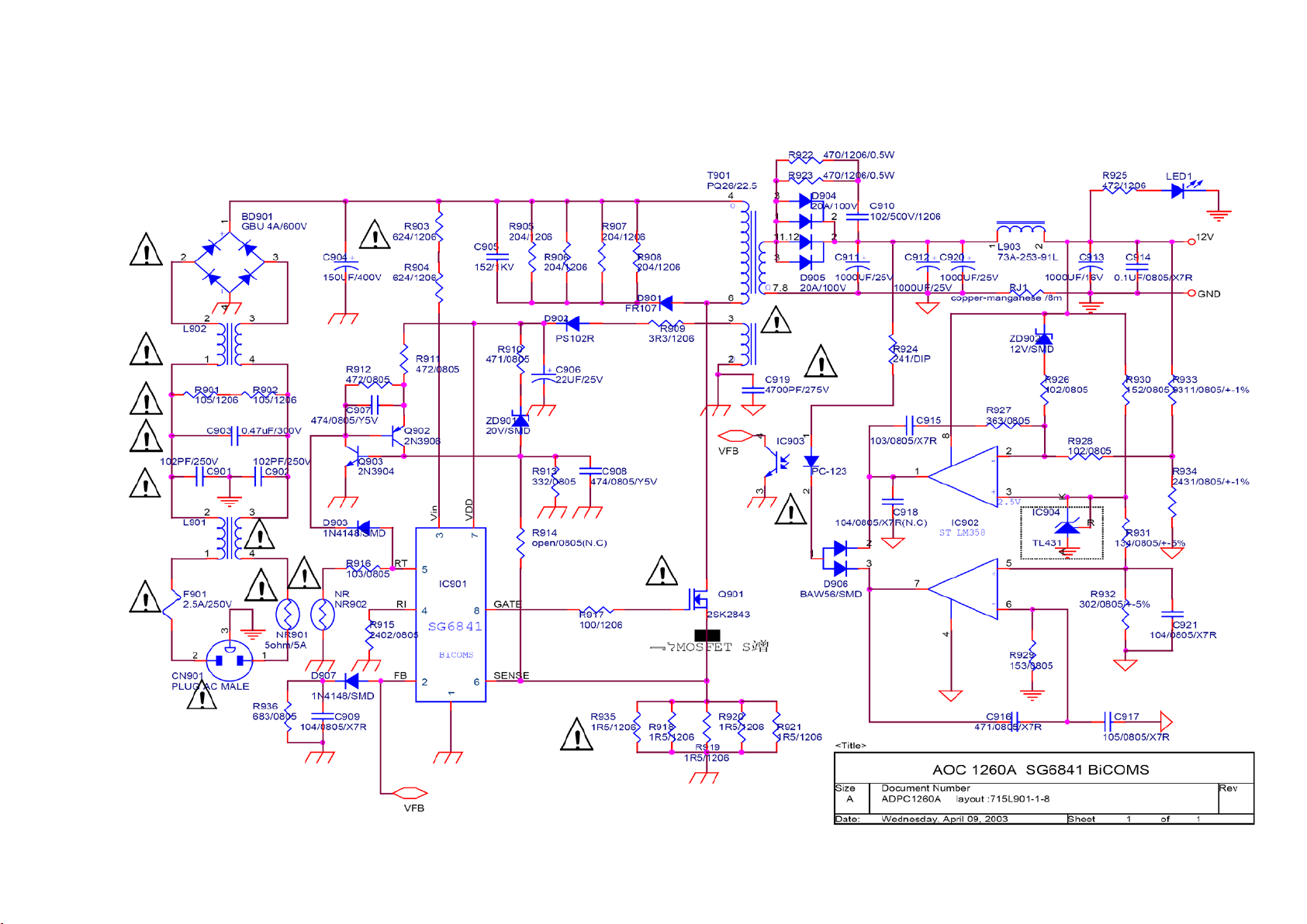
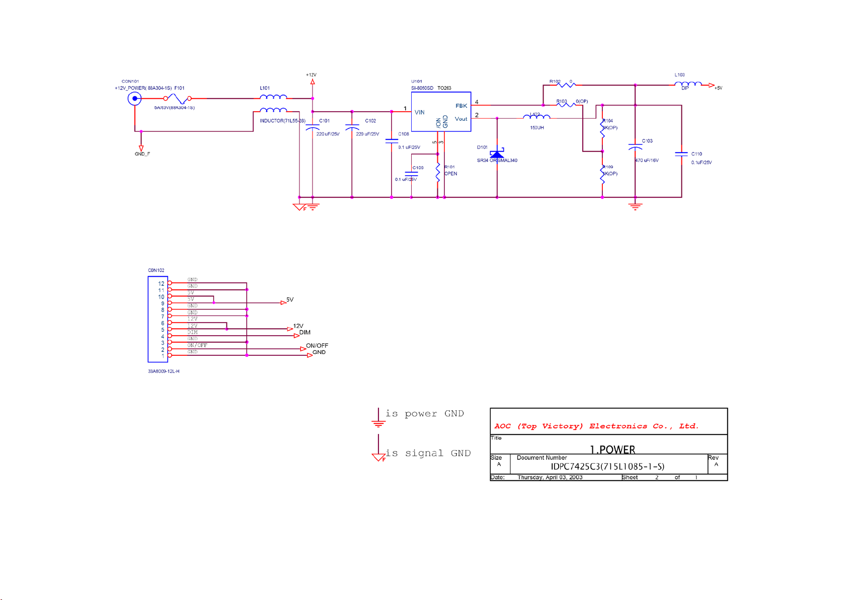
6.2 Power Board
Adapter
AOC 193FW (+)
24
Page 25
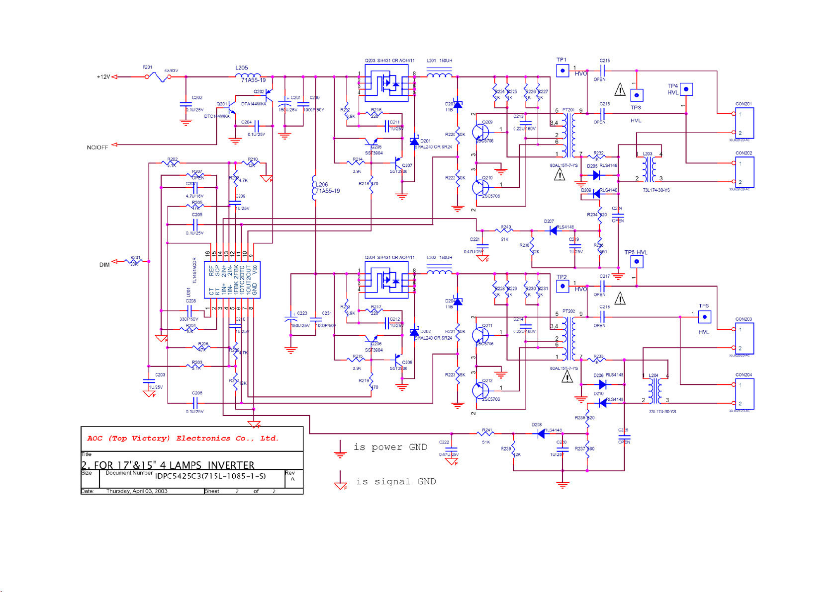
Inverter
AOC 193FW (+)
25
Page 26
AOC 193FW (+)
26
Page 27
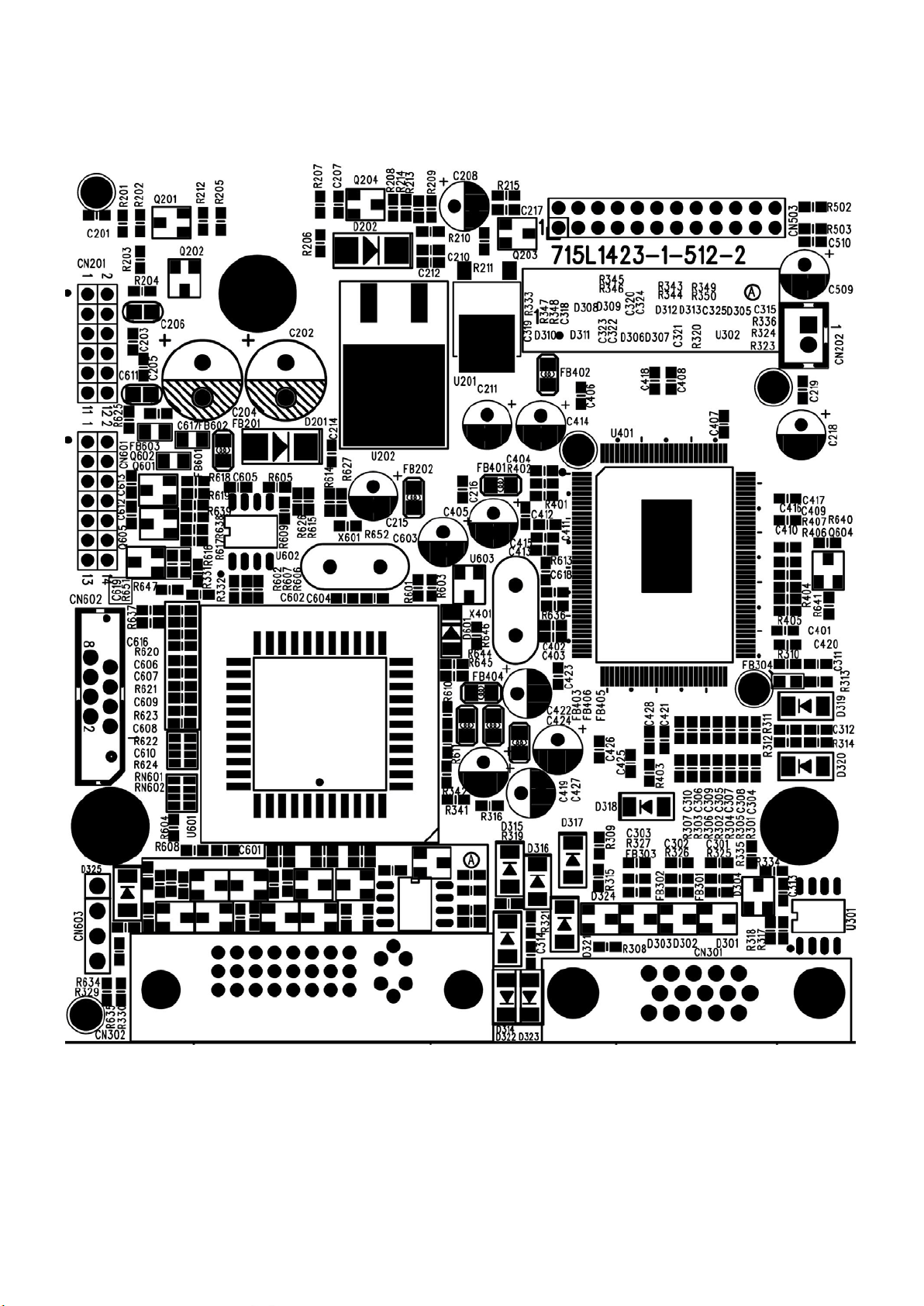
7. PCB Layout
7.1 Main Board
715L1423-1-512-2
AOC 193FW (+)
27
Page 28
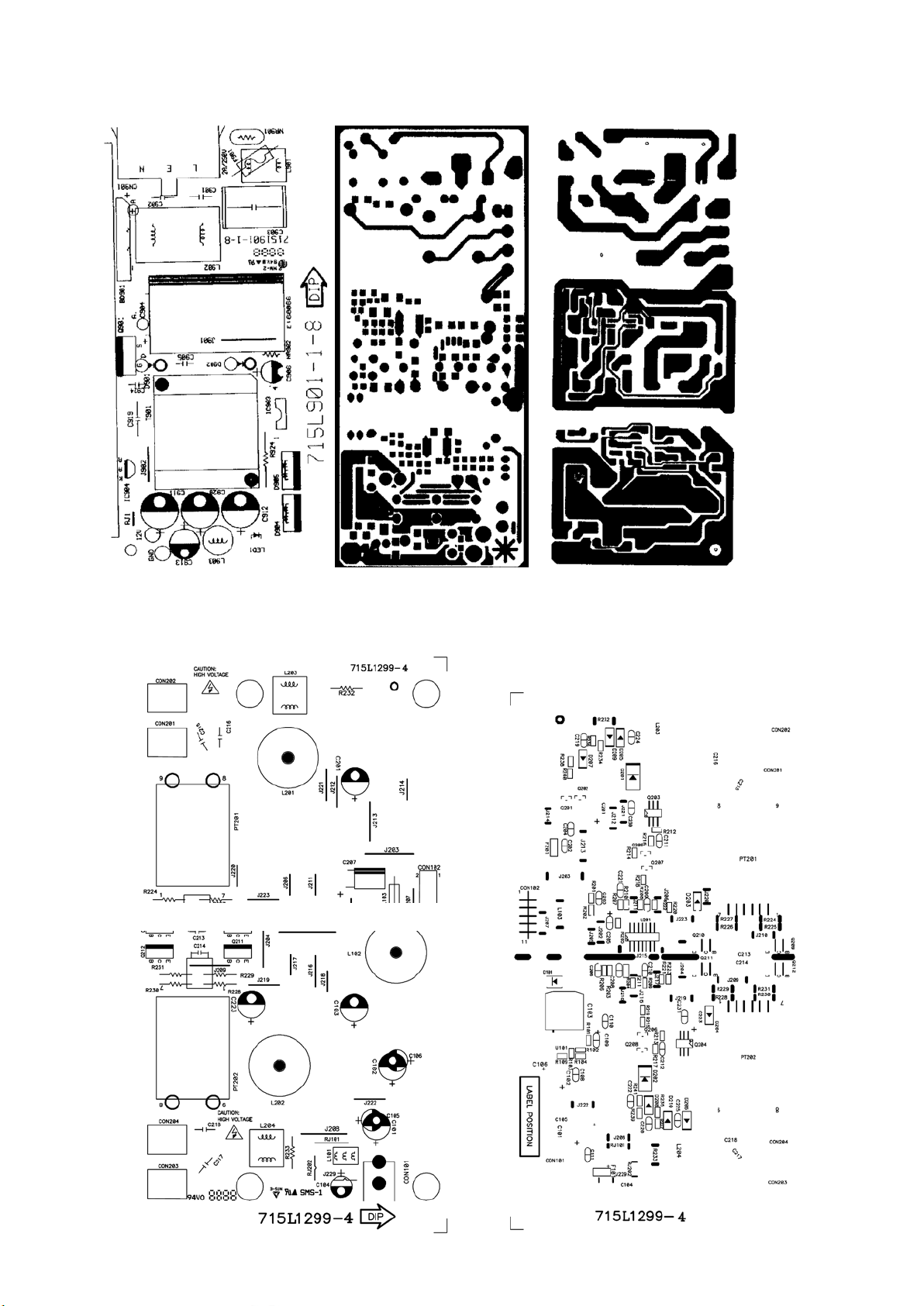
7.2 Adapter Board
715V901-1-8
AOC 193FW (+)
7.3 Inverter Board
715L1299-4
28
Page 29

8. Maintainability
8.1 Equipments and Tools Requirement
1. Voltmeter.
2. Oscilloscope.
3. Pattern Generator.
4. DDC T ool with an IBM Compatible Computer.
5. Alignment Tool.
6. LCD Color Analyzer.
7. Service Manual.
8. User Manual.
AOC 193FW (+)
29
Page 30
8.2 Trouble Shooting
8.2.1 Main Board
1. No Screen Appear
Measured CN201 pin5/6 = 12V?
Measured CN201 pin 9/10= 5V?
Measured U202 pin 2= 3.3V?
AOC 193FW (+)
Check Correspondent component.
Is there any shortage or cold solder?
Yes, all DC level exist
Disconnected the Signal cable (Loose the
Signal cable) , Is the screen show “Cable N ot
Connected”?
Show noting
Connected the Signal cable
again
Led Orange
Led Green
Check the Wire-Harness from CN503
Check Panel-Power Circuit Block
OK, Wire tight enough
Check U401 Data-output Block
OK, Panel Power OK
OK
Yes. There is OSD show
Connected the Signal cable again,
Check LED status.
Check Power switch is in Power-on
status, and check if Po wer switch had
been stuck?
OK, Keyboard no stuck
Measured RGB (R301, R302, R303) H,V
Input at U401 pin 37,38 ,was there have
signal ?
OK, input Normal
Measured Crystal X401 (14.318MHz)
OK, clock normal
Led Green
Replace U601
Led orange
Check Correspondent
component short/open
(Protection Diode)
NG
Replace Power board and Check
Inverter control relative circuit
Replace U401
Re-do White balance adjust
Note:1. If replace “MAIN-BOARD”, Please re-do “DDC-content” programmed & “WHITE-Balance”.
2. If replace “Power Board” only, Please re-do “ WHITE-Balance”
30
OK
Page 31

2. Panel Power Circuit
OK
NG
Check C509 should have response from 0V to 5V
When we switch the power switch from off to on
Check Q204, Q203 is broken or CN503 solder abnormal?
NG
AOC 193FW (+)
Measured X601 waveform is normal?
NG
OK
Replace U601
Replace X601
(24MHz)
NG
OK
Replace Panel
3. Inverter Control Relative Circ u it
Measured the inverter connector
CN102
Pin1 on/off control=5V (on)
Pin2 PWM signal control dim 0V-5V
OK
Replace Power board
& Re-do white balance
Replace Q204, Q203 or re-solder CN503
Check the Bklt-On relative circuit, R201, Q201,
NG
In normal operation, when LED =green,
Base of Q201 should =0 v,
In saving mode, when LED=orange,
Base of Q201 should =5 v,
OK
Replace U201
31
Page 32

4. U4-Data Output
Measured X401 waveform
AOC 193FW (+)
normal?
NG
Replace X401(14.318MHz)
OK
Check TSU56AK (U401)
Signal output (PIN102-103, 106-113,118-125,128,1)
Is the waveform ok?
OK
Check relative circuit to panel
Check HS/VS input signal are normal?
NG
NG
Check relative component
OK
Replace U401
32
Page 33

8.2.2 Power/Inverter Board
No Backlight
AOC 193FW (+)
Check C201 (+) =12V
OK
NG
Check F201 or power section
Check ON/OFF signal
OK
NG
Check main board
Check U201 pin9=12V
OK
NG
Check Q201, Q202
Check U201 PIN1 triangular wave i s normal
OK
NG
Check R204,C208, U201
Connect PIN4 and PIN7 of U201 if the picture is normal
OK
NG
Replace U201
Check the feedback circuit
NG
OK
Check D210, D208, C222, R 241,
C220 and so on
Check connecter & lamp
33
Page 34

8.2.3 Keypad Board
AOC 193FW (+)
OSD is unstable or not working
N
Is Key Pad Board connecting normally?
Connect Key Pad Board
Is Button Switch normally?
Is Key Pad Board normally?
Check Main Board
Y
N
Replace Button Switch
Y
N
Replace Key Pad Board
Y
34
Page 35

AOC 193FW (+)
9. White-Balance, Luminance adjustment
Approximately 30 minutes should be allowed for warm up before proceeding white balance adjustment.
Before started adjust white balance , pl eas e set the Ch roma-7120 MEM Channel 9 to 6500 color, and
MEM Channel 10 to 7800 color. ( our 6500 parameter is x = 313 ±28, y = 329 ±28, Y = 200 ±10
cd/m2 , 7800 parameter is x = 296 ±28, y = 311 ±28, Y = 200 ±10 cd/m2)
How to setting MEM channel you can reference to chroma 7120 user guide or simple use “ SC” key and
“ NEXT” Key to modify xyY value and use “ID” key to modify the TEXT description Follo wing is the proce dur e
to do white-balance adjust .
Press MENU button during 2 seconds along with press Power button will activate the factory mode, then MCU
will do AUTO LEVEL automatically. Meanwhile press MENU the OSD screen will located at left top of panel.
1. Bias adjustment :
Set the contrast
Adjust the Brightness
2. Gain adjustment :
Move cursor to “-F-” and press MENU key
A. adjust 6500 color-temperature
1. Switch the chroma-7120 to RGB-mode (with press “MODE” button )
2. Switch the MEM channel to Channel9 ( with up or down arrow on chroma 7120 )
3. The LCD-indicator on chroma 7120 will show x = 313 ±28, y = 329 ±28,Y = 200 ±10 cd/m2
4. Adjust the RED of color1 on factory window until chroma 7120 indicator reached the value R=100
5. Adjust the GREEN of color1 on factory, until chroma 7120 indicator reached G=100
6. Adjust the BLUE of color1 on factory, until chroma 7120 indicator reached B=100
to 50.
to 50.
7. Repeat above procedure ( item 5,6,7) until chroma 7120 RGB value meet the tolerance =100±2
B. Adjust 7800 color-temperature
1. Switch the chroma-7120 to RGB-mode (with press “MODE” button )
2. Switch the MEM channel to Channel10 ( with up or down arrow on chroma 7120 )
3.The LCD-indicator on chroma 7120 will show x = 296±28, y = 3 11±28, Y = 200 ±10 cd/m2
4. Adjust the RED of color2 on factory window until chroma 7120 indicator reached the value R=100
5. Adjust the GREEN of color2 on factory, until chroma 7120 indicator reached G=100
6. Adjust the BLUE of color2 on factory, until chroma 7120 indicator reached B=100
7. Repeat above procedure ( item 5,6,7) until chroma 7120 RGB value meet the tolerance =100±2
35
Page 36

10. EDID Content
Analog
00 01 02 03 04 05 06 07 08 09 10 11 12 13 14 15
0: 00 FF FF FF FF FF FF 00 05 E3 80 19 9F 58 0D 00
16: 31 0F 01 03 68 28 19 78 2F 6A C6 A1 59 4B 99 23
32: 17 4F 59 BF EF 00 71 4F 81 40 81 80 95 00 01 01
48: 01 01 01 01 01 01 9A 29 A0 D0 51 84 22 30 50 98
64: 36 00 98 FF 10 00 00 1C 00 00 00 FF 00 33 31 32
80: 36 35 34 39 38 37 34 36 35 35 00 00 00 FD 00 37
96: 4B 1E 53 0E 00 0A 20 20 20 20 20 20 00 00 00 FC
112: 00 31 39 33 46 57 0A 20 20 20 20 20 20 20 00 5D
Digital
AOC 193FW (+)
00 01 02 03 04 05 06 07 08 09 10 11 12 13 14 15
0: 00 FF FF FF FF FF FF 00 05 E3 80 19 A7 5F 0D 00
16: 33 0F 01 03 80 28 19 78 2F 6A C6 A1 59 4B 99 23
32: 17 4F 59 BF EF 00 71 4F 81 40 81 80 95 00 01 01
48: 01 01 01 01 01 01 9A 29 A0 D0 51 84 22 30 50 98
64: 36 00 98 FF 10 00 00 1C 00 00 00 FF 00 33 32 31
80: 34 36 35 39 38 37 36 34 35 35 00 00 00 FD 00 37
96: 4B 1E 53 0E 00 0A 20 20 20 20 20 20 00 00 00 FC
112: 00 31 39 33 46 57 0A 20 20 20 20 20 20 20 00 34
36
Page 37

11. BOM List
T982KM2HDBAON
Location Part No. Description
ADPC1260AE LCD ADAPTER BOARD ASS'Y
CBPC982KM2CN CONVERSION BOARD
IDPC1942AUA1 INVERTER DC BOARD
2G6014 1 SCREW
12G6204 1 RUBBER
12G6300 11 RUBBER
15G6231 3 MAIN FRAME
15G6232 2 PANEL-SIDE-BKT
15G6335 1 SHIELD
26G 800504 3 BARCODE
34G6346AOP 1B BEZEL
40G 19E615 8B RATING LABEL
AOC 193FW (+)
40G 457615 9A 8MS LABEL
40G 58162435A LABEL
41G 68615 4B TCO'99 CARD
41G190061535A MANUAL
41G780061585C WARRANTY CAR D
44G3933615 1A CARTON
44G3952 1 EPS (L)
44G3952 2 EPS(R)
45G 76 28 RN PE BAG FO MANUAL/BASE
45G 88606 PE BAG FOR BASE
45G 88609 21 EPE COVER
45G 88618 55 OUT PE BAG
45G 88626 4 PE BAG FOR MONITOR
50G 600 2 HANDLE1
50G 600 3 HANDLE2
52G 1185 MIDDLE TAPE FOR CARTON
52G 1186 SMALL TAPE
52G 1209 A ALUMINIUM TAPE
52G 1211 A ALUMINIUM TAPE
52G6020 17 PROTECT FILM
52G6025 11946 MYLAR
52G6025 11980 MYLAR
77GB800SRG G MEMBRANE KEY PADS HORII
89G 715CAA D SIGNAL CABLE
37
Page 38

89G 745GAA A V DVI CABLE
89G414A15N YH POWER CORD
95G8018 30650 LVDS
M1G 130 6128 SCREW
M1G 330 6 47 SCREW
M1G1130 6128 SCREW
705L982KP34008 19" LCD STAND ASS'Y
750LLM90A11 11 CMO 19" A1-L01 PANEL
AM1G1740 10 47 SCREW
C911 67G215C102 4K LOW&E.S.RE.C 105
C912 67G215C102 4K LOW&E.S.RE.C 105
C920 67G215C102 4K LOW&E.S.RE.C 105
33T6007 1 LENS
40T 154501 1 HI-POT GND LABEL FOR MO
40T 581700 6A LABEL
AOC 193FW (+)
40T 500B 615 1C ID LABEL
45T 88525 E PE B AG
52T 1211 A ADHESIVE TYPE
IC903 56T 139 3A PC123Y22FZOF
NR901 61T 58050 WT NTC THERMISTOR
C903 63T 107474 HS 0.47UF +-20% 275VAC
C919 65G306M4722BP 4700PF +-20% 400VAC
C901 65V305M1022E3 1000PF +-20% 400VAC BY
C902 65V305M1022E3 1000PF +-20% 400VAC BY
C904 67T 30515114H 150UF 400V HERMEI
71T 55500 S FERRITE BEAD 3.5*3*1.3
L901 73L 174 29LSG CHOKE COIL
L902 73L 174 31LSG CHOKE COIL
L903 73T 253 91 H CHOKE COIL
T901 80LL17T 5LSG ADAPTOR BY LISHIN
LED1 81T 2 3 2P LED
F901 84V 53 2 250V/2A
CN901 87T 501 11 RF AC SOCKET
89T 171513 1.2M 16AWG 1185 STYLE
90T6063500 T HEAT SINK
90T6083 1 HEAT SINK
BD901 93T 50460 16 U4KB80R
D904 93T 60237 SRF20100C
D905 93T 60237 SRF20100C
38
Page 39

D901 93T 6026T52T FR107
D902 93T 6038T52T FR103
RJ1 95T 90 26 WIRE HARNESS
A 95T 205430322 WIRE HARNESS
96T 29 8 TUBE
M1T 330 8128 SCREW M3X8
W33T6045 B T TOP COVER
W33T6046 B T COVER
705L 990 57 01 Q901 ASS'Y
IC902 56T 192 10 LM358DT
IC901 56T 379 33 SG6841SZ
Q903 57T 417 4 CHIP PMBS3904 BY PHILIP
Q902 57T 417 6 PMBS3906/PHILIPS-SMT
R926 61V0805102 CHIPR 1K OHM +-5% 1/8W
R928 61V0805102 CHIPR 1K OHM +-5% 1/8W
AOC 193FW (+)
R930 61V0805152 CHIPR 1.5K OHM +-5% 1/8
R929 61V0805153 CHIPR 15K OHM+-5% 1/8W
R931 61V0805154 CHIP 150KOHM 5% 1/8W
R915 61V0805240 2F CHIP 24KOHM 1% 1/8W
R934 61V0805243 1F CHIP 2.43K OHM 1/8W 1%
R913 61V0805332 CHIP 3.3K OHM +-5% 1/8W
R932 61V0805332 CHIP 3.3K OHM +-5% 1/8W
R927 61V0805363 CHIP 36KOHM 1/8W
R910 61V0805471 CHIPR 470 OHM+-5% 1/8W
R911 61V0805472 CHIRP 4.7K OHM +-5% 1/8
R912 61V0805472 CHIRP 4.7K OHM +-5% 1/ 8
R936 61V0805683 CHIPR 68K OHM+-5% 1/8W
R933 61V0805931 1F CHIP 9.31K OHM 1/8W 1%
R917 61V1206100 CHIP 10 OHM 1/8W
R901 61V1206105 CHIP 1MOHM 5% 1/4W
R902 61V1206105 CHIP 1MOHM 5% 1/4W
R918 61V1206159 CHIP1.5OHM 5% 1/4W
R919 61V1206159 CHIP1.5OHM 5% 1/4W
R920 61V1206159 CHIP1.5OHM 5% 1/4W
R921 61V1206159 CHIP1.5OHM 5% 1/4W
R935 61V1206159 CHIP1.5OHM 5% 1/4W
R905 61V1206204 CHIP 200KOHM 1/4W
R906 61V1206204 CHIP 200KOHM 1/4W
R907 61V1206204 CHIP 200KOHM 1/4W
39
Page 40

R908 61V1206204 CHIP 200KOHM 1/4W
R922 61V1206470 CHIP 47OHM 5% 1/4W
R923 61V1206470 CHIP 47OHM 5% 1/4W
R925 61V1206472 CHIP 4.7KOHM 5% 1/4W
R909 61V1206519 CHIPR 5.1OHM +-5% 1/4W
R903 61V1206624 CHIP 620K 5% 1/4W
R904 61V1206624 CHIP 620K 5% 1/4W
C915 65T0805103 22 CHIP 0.01UF 25V X7R 080
C909 65T0805104 22 0.1U F +-10% 25 V X7R 080
C914 65T0805104 22 0.1U F +-10% 25 V X7R 080
C921 65T0805104 22 0.1U F +-10% 25 V X7R 080
C917 65T0805105 12 1UF +-10% 6V X7R
C916 65T0805221 21 220PF 25V 5%
C907 65T0805474 27 CHIP 0.47UF 25V Y5V
C908 65T0805474 27 CHIP 0.47UF 25V Y5V
AOC 193FW (+)
C923 65T1206101 71 100PF 500V 1/8W
C922 65T1206102 32 CHIP 1000PF/XTR +-5%
C910 65T1206102 72 CHIP 1000PF 500V X7R
D906 93T 64 38 P DIODE
D903 93T 6432S IN4148W
D907 93T 6432S IN4148W
ZD902 93T 39S 3 T BZT52-C11
ZD901 93T 39S 12 T RLZ20B LLDS
T901 6G 31502 1.5MM RIVET
715V 901 1 8 PCB BOARD
R924 61T 17224152T 240 OHM 5% 1/4W
C906 67T 305220 7T 22uf 50v
IC904 56T 158 4 T H431BA
C924 65T 1K101 5T6921 100PF /1KV
C905 65T 1K152 1T6052 1.5nF /1K Y5P+-10%
Q901 57T 724 8 2SK2843
90T6062 1 HEAT SINK
M1T1030 5128 SCREW
CN602 33G8019 8C FPC/FFC CONN
CN201 33G8027 12 WAFER 2*6P 2.0MM R/A
CN503 33G802724B H WAFER
40G 45762412B CBPC LABEL
C202 67G215V221 4R LOW E.S.R 220UF +/-20%
C204 67G215V221 4R LOW E.S.R 220UF +/-20%
40
Page 41

C211 67G215V470 4R LOW E.S.R 47UF +/-20% 2
C215 67G215V470 4R LOW E.S.R 47UF +/-20% 2
C208 67G215Y100 7R LOW E.S.R 10UF +/-20% 5
C405 67G215Y100 7R LOW E.S.R 10UF +/-20% 5
C414 67G215Y100 7R LOW E.S.R 10UF +/-20% 5
C419 67G215Y100 7R LOW E.S.R 10UF +/-20% 5
C422 67G215Y100 7R LOW E.S.R 10UF +/-20% 5
C424 67G215Y100 7R LOW E.S.R 10UF +/-20% 5
C427 67G215Y100 7R LOW E.S.R 10UF +/-20% 5
C603 67G215Y100 7R LOW E.S.R 10UF +/-20% 5
C509 67G215Y2207RV RUBYCON 50V 22UF
CN301 88G 35315F H D-SUB 15PIN
CN302 88G 35424F H DV1 CONNECTOR 24PIN
U401 90G 444 1 HEAT SINK
X601 93G 22 45 H 24MHZ/30PF/49US
AOC 193FW (+)
X401 93G 22 53 CRYSTAL 14.318MHzHC-49U
40G 457624 1B LABEL-CPU
U401 56G 562 82 TSU56AK-LF
U202 56G 563 7 AIC1084-33PM
U201 56G 563 31 AI1117D-1.8-EI
U301 56G1133 34 M24C02-WMN6TP
U302 56G1133 34 M24C02-WMN6TP
U602 56G1133 56 M24C16-WMN6TP
U601 56L1125543MA7 MTV512 MV 44 PIN-PLCC
Q201 57G 417 4 PMBS3904/PHILIPS-SMT(04
Q202 57G 417 4 PMBS3904/PHILIPS-SMT(04
Q204 57G 417 4 PMBS3904/PHILIPS-SMT(04
Q605 57G 417 4 PMBS3904/PHILIPS-SMT(04
Q601 57G 417 6 PMBS3906/PHILIPS-SMT(06
Q602 57G 417 6 PMBS3906/PHILIPS-SMT(06
Q203 57G 763 1 A03401 SOT23 BY AOS(A1)
RN601 61L 125103 8 CHIP AR 8P4R 10KOHM +-5
RN602 61L 125103 8 CHIP AR 8P4R 10KOHM +-5
FB301 61L0603000 RST SM 0603 JUMP MAX 0R
FB302 61L0603000 RST SM 0603 JUMP MAX 0R
FB303 61L0603000 RST SM 0603 JUMP MAX 0R
R209 61L0603000 RST SM 0603 JUMP MAX 0R
R341 61L0603000 RST SM 0603 JUMP MAX 0R
R342 61L0603000 RST SM 0603 JUMP MAX 0R
41
Page 42

R502 61L0603000 RST SM 0603 JUMP MAX 0R
R637 61L0603000 RST SM 0603 JUMP MAX 0R
R343 61L0603100 CHIP 10 OHM 1/10W
R344 61L0603100 CHIP 10 OHM 1/10W
R345 61L0603100 CHIP 10 OHM 1/10W
R346 61L0603100 CHIP 10 OHM 1/10W
R347 61L0603100 CHIP 10 OHM 1/10W
R348 61L0603100 CHIP 10 OHM 1/10W
R349 61L0603100 CHIP 10 OHM 1/10W
R350 61L0603100 CHIP 10 OHM 1/10W
R309 61L0603101 RST SM 0603 RC0603 100R
R312 61L0603101 RST SM 0603 RC0603 100R
R315 61L0603101 RST SM 0603 RC0603 100R
R316 61L0603101 RST SM 0603 RC0603 100R
R319 61L0603101 RST SM 0603 RC0603 100R
AOC 193FW (+)
R320 61L0603101 RST SM 0603 RC0603 100R
R402 61L0603101 RST SM 0603 RC0603 100R
R608 61L0603101 RST SM 0603 RC0603 100R
R609 61L0603101 RST SM 0603 RC0603 100R
R636 61L0603101 RST SM 0603 RC0603 100R
R639 61L0603101 RST SM 0603 RC0603 100R
R203 61L0603102 RST SM 0603 RC0603 1K P
R311 61L0603102 RST SM 0603 RC0603 1K P
R332 61L0603102 RST SM 0603 RC0603 1K P
R624 61L0603102 RST SM 0603 RC0603 1K P
R202 61L0603103 RST SM 0603 RC0603 10K
R204 61L0603103 RST SM 0603 RC0603 10K
R208 61L0603103 RST S M 0603 RC0603 10K
R211 61L0603103 RST SM 0603 RC0603 10K
R308 61L0603103 RST SM 0603 RC0603 10K
R317 61L0603103 RST SM 0603 RC0603 10K
R318 61L0603103 RST SM 0603 RC0603 10K
R321 61L0603103 RST SM 0603 RC0603 10K
R323 61L0603103 RST S M 0603 RC0603 10K
R324 61L0603103 RST SM 0603 RC0603 10K
R331 61L0603103 RST SM 0603 RC0603 10K
R335 61L0603103 RST SM 0603 RC0603 10K
R336 61L0603103 RST SM 0603 RC0603 10K
R404 61L0603103 RST SM 0603 RC0603 10K
42
Page 43

R405 61L0603103 RST SM 0603 RC0603 10K
R406 61L0603103 RST SM 0603 RC0603 10K
R407 61L0603103 RST SM 0603 RC0603 10K
R601 61L0603103 RST SM 0603 RC0603 10K
R602 61L0603103 RST SM 0603 RC0603 10K
R603 61L0603103 RST SM 0603 RC0603 10K
R604 61L0603103 RST SM 0603 RC0603 10K
R605 61L0603103 RST SM 0603 RC0603 10K
R606 61L0603103 RST SM 0603 RC0603 10K
R607 61L0603103 RST SM 0603 RC0603 10K
R613 61L0603103 RST SM 0603 RC0603 10K
R644 61L0603103 RST SM 0603 RC0603 10K
R645 61L0603103 RST SM 0603 RC0603 10K
R646 61L0603103 RST SM 0603 RC0603 10K
R652 61L0603103 RST SM 0603 RC0603 10K
AOC 193FW (+)
R617 61L0603121 CHIPR 120 OHM 1/10W
R618 61L0603121 CHIPR 120 OHM 1/10W
R201 61L0603203 CHIPR 20K OHM+-5% 1/10W
R610 61L0603221 RST SM 0603 RC0603 220R
R611 61L0603221 RST SM 0603 RC0603 220R
R313 61L0603222 RST SM 0603 RC0603 2K2
R314 61L0603222 RST SM 0603 RC0603 2K2
R647 61L0603223 CHIPR 22K OHM +-5% 1/10
R301 61L0603330 CHIPR 33 OHM +-5% 1/10W
R302 61L0603330 CHIPR 33 OHM +-5% 1/10W
R303 61L0603330 CHIPR 33 OHM +-5% 1/10W
R403 61L0603390 0F CHIP 390 OHM 1/10W 1%
R304 61L0603471 CHIPR 470 OHM+-5% 1/10W
R620 61L0603471 CHIPR 470 OHM+-5% 1/10W
R621 61L0603471 CHIPR 470 OHM+-5% 1/10W
R622 61L0603471 CHIPR 470 OHM+-5% 1/10W
R623 61L0603471 CHIPR 470 OHM+-5% 1/10W
R205 61L0603472 RST SM 0603 RC0603 4K7
R207 61L0603472 RST SM 0603 RC0603 4K7
R212 61L0603472 RST SM 0603 RC0603 4K7
R616 61L0603472 RST SM 0603 RC0603 4K7
R619 61L0603472 RST SM 0603 RC0603 4K7
R305 61L0603510 CHIP 51 OHM 5% 1/10W
R306 61L0603510 CHIP 51 OHM 5% 1/10W
43
Page 44

R307 61L0603510 CHIP 51 OHM 5% 1/10W
R215 61L0603513 CHIP 51K OHM 1/10W
R310 61L0603561 CHIP 560 OHM 1/10W
R325 61L0603750 RST SM 0603 RC22H 75R P
R326 61L0603750 RST SM 0603 RC22H 75R P
R327 61L0603750 RST SM 0603 RC22H 75R P
R503 61L0603750 RST SM 0603 RC22H 75R P
R651 61L0603912 CHIPR 9.1KOHM +-5% 1/10
C307 65G0603102 32 1000PF +-10% 50V X7R
C606 65G0603102 32 1000PF +-10% 50V X7R
C607 65G0603102 32 1000PF +-10% 50V X7R
C608 65G0603102 32 1000PF +-10% 50V X7R
C609 65G0603102 32 1000PF +-10% 50V X7R
C610 65G0603102 32 1000PF +-10% 50V X7R
C201 65G0603104 32 CHIP 0.1UF 50V X7R
AOC 193FW (+)
C203 65G0603104 32 CHIP 0.1UF 50V X7R
C205 65G0603104 32 CHIP 0.1UF 50V X7R
C207 65G0603104 32 CHIP 0.1UF 50V X7R
C210 65G0603104 32 CHIP 0.1UF 50V X7R
C212 65G0603104 32 CHIP 0.1UF 50V X7R
C214 65G0603104 32 CHIP 0.1UF 50V X7R
C216 65G0603104 32 CHIP 0.1UF 50V X7R
C217 65G0603104 32 CHIP 0.1UF 50V X7R
C313 65G0603104 32 CHIP 0.1UF 50V X7R
C314 65G0603104 32 CHIP 0.1UF 50V X7R
C315 65G0603104 32 CHIP 0.1UF 50V X7R
C318 65G0603104 32 CHIP 0.1UF 50V X7R
C319 65G0603104 32 CHIP 0.1UF 50V X7R
C320 65G0603104 32 CHIP 0.1UF 50V X7R
C321 65G0603104 32 CHIP 0.1UF 50V X7R
C322 65G0603104 32 CHIP 0.1UF 50V X7R
C323 65G0603104 32 CHIP 0.1UF 50V X7R
C324 65G0603104 32 CHIP 0.1UF 50V X7R
C325 65G0603104 32 CHIP 0.1UF 50V X7R
C401 65G0603104 32 CHIP 0.1UF 50V X7R
C404 65G0603104 32 CHIP 0.1UF 50V X7R
C406 65G0603104 32 CHIP 0.1UF 50V X7R
C407 65G0603104 32 CHIP 0.1UF 50V X7R
C408 65G0603104 32 CHIP 0.1UF 50V X7R
44
Page 45

C409 65G0603104 32 CHIP 0.1UF 50V X7R
C410 65G0603104 32 CHIP 0.1UF 50V X7R
C411 65G0603104 32 CHIP 0.1UF 50V X7R
C412 65G0603104 32 CHIP 0.1UF 50V X7R
C413 65G0603104 32 CHIP 0.1UF 50V X7R
C415 65G0603104 32 CHIP 0.1UF 50V X7R
C416 65G0603104 32 CHIP 0.1UF 50V X7R
C417 65G0603104 32 CHIP 0.1UF 50V X7R
C418 65G0603104 32 CHIP 0.1UF 50V X7R
C420 65G0603104 32 CHIP 0.1UF 50V X7R
C421 65G0603104 32 CHIP 0.1UF 50V X7R
C423 65G0603104 32 CHIP 0.1UF 50V X7R
C425 65G0603104 32 CHIP 0.1UF 50V X7R
C426 65G0603104 32 CHIP 0.1UF 50V X7R
C428 65G0603104 32 CHIP 0.1UF 50V X7R
AOC 193FW (+)
C510 65G0603104 32 CHIP 0.1UF 50V X7R
C601 65G0603104 32 CHIP 0.1UF 50V X7R
C618 65G0603104 32 CHIP 0.1UF 50V X7R
C619 65G0603104 32 CHIP 0.1UF 50V X7R
C402 65G0603220 31 CER1 0603 NP0 50V 22P P
C403 65G0603220 31 CER1 0603 NP0 50V 22P P
C602 65G0603220 31 CER1 0603 NP0 50V 22P P
C312 65G0603221 31 CER1 0603 NP0 50V 220P
C605 65G0603224 17 CAP:CER 0.22UF-20%-80%
C604 65G0603270 31 27PF 50V NPO
C311 65G0603330 31 CER1 0603 NP0 50V 33P P
C304 65G0603473 32 CHIP 0.047UF 50V X7R
C305 65G0603473 32 CHIP 0.047UF 50V X7R
C306 65G0603473 32 CHIP 0.047UF 50V X7R
C308 65G0603473 32 CHIP 0.047UF 50V X7R
C309 65G0603473 32 CHIP 0.047UF 50V X7R
C310 65G0603473 32 CHIP 0.047UF 50V X7R
C206 65G0805105 22 CHIP 1UF 25V X7R 0805
FB202 71G 56Z601 CHIP BEAD 600 OHM 0805
FB401 71G 56Z601 CHIP BEAD 600 OHM 0805
FB402 71G 56Z601 CHIP BEAD 600 OHM 0805
FB403 71G 56Z601 CHIP BEAD 600 OHM 0805
FB404 71G 56Z601 CHIP BEAD 600 OHM 0805
FB405 71G 56Z601 CHIP BEAD 600 OHM 0805
45
Page 46

FB406 71G 56Z601 CHIP BEAD 600 OHM 0805
FB304 71G 59B431 BK1608 HW 431
D314 93G 39147 TZMC5V6
D315 93G 39147 TZMC5V6
D316 93G 39147 TZMC5V6
D318 93G 39147 TZMC5V6
D319 93G 39147 TZMC5V6
D320 93G 39147 TZMC5V6
D321 93G 39147 TZMC5V6
D322 93G 39147 TZMC5V6
D323 93G 39147 TZMC5V6
D325 93G 39147 TZMC5V6
D304 93G 64 42 P BAV70 SOT-23
D305 93G 64 42 P BAV70 SOT-23
C301 93G 64 49 SU EGA10603 V05
AOC 193FW (+)
C302 93G 64 49 SU EGA10603 V05
C303 93G 64 49 SU EGA10603 V05
D601 93G 6432V LL4148-GS08
D301 93G 6433P BAV99 SOT-23
D302 93G 6433P BAV99 SOT-23
D303 93G 6433P BAV99 SOT-23
D306 93G 6433P BAV99 SOT-23
D307 93G 6433P BAV99 SOT-23
D308 93G 6433P BAV99 SOT-23
D309 93G 6433P BAV99 SOT-23
D310 93G 6433P BAV99 SOT-23
D311 93G 6433P BAV99 SOT-23
D312 93G 6433P BAV99 SOT-23
D313 93G 6433P BAV99 SOT-23
D324 93G 6433P BAV99 SOT-23
D317 93G 39S 39 T MLL5234B
D201 93G1004 3 SS14
D202 93G1020 1 S GS1D
715L1423 1512 2 PCB
J229 71G 55 9 T FERRITE BEAD
CON201 33G8021 2D AC CONN.2P R/A 87210-0236
CON202 33G8021 2D AC CONN.2P R/A 87210-0236
CON203 33G8021 2D AC CONN.2P R/A 87210-0236
CON204 33G8021 2D AC CONN.2P R/A 87210-0236
46
Page 47

40G 45762412B CBPC LABEL
P051 51G 6503 RTV
Q209 57G 761501 BTC5706I3
Q210 57G 761501 BTC5706I3
Q211 57G 761501 BTC5706I3
Q212 57G 761501 BTC5706I3
C213 63G210J1842A2 PMS 0.18UF 250V
C214 63G210J1842A2 PMS 0.18UF 250V
C215 65G 3J2206ET 22PF 5% SL 3KV TDK
C216 65G 3J2206ET 22PF 5% SL 3KV TDK
C217 65G 3J2206ET 22PF 5% SL 3KV TDK
C218 65G 3J2206ET 22PF 5% SL 3KV TDK
C207 67G 305330 7T 33UF 105
C103 67G215B471 3H 470UF 16V LTR471M1CF11V
C201 67G215C151 4K LOW E,S,R 150UF +-20% 2
AOC 193FW (+)
C223 67G215C151 4K LOW E,S,R 150UF +-20% 2
C101 67G215V221 4K EC 220F 25V
C102 67G215V221 4K EC 220F 25V
L101 71G 55 28 FERRITE BEAD 7.62*5.08*
L102 73G 253138 Y CHOKE BY
L201 73G 253138 Y CHOKE BY
L202 73G 253138 Y CHOKE BY
CON101 88G 3041CF DC JACK
CON102 95G8014 6512 WIRE HARNESS
U101 56G 563 11 S1-8050SD
U201 56G 608 1 TL1451ACD
Q205 57G 417 4 PMBS3904/PHILIPS-SMT(04
Q206 57G 417 4 PMBS3904/PHILIPS-SMT(04
Q207 57G 417 6 PMBS3906/PHILIPS-SMT(06
Q208 57G 417 6 PMBS3906/PHILIPS-SMT(06
Q202 57G 760 4 DT A144WKA BY ROHM SMT
Q201 57G 760 5 DTC144WKA BY ROHM SMT
Q203 57G 763 3 AO4411 SO-8
Q204 57G 763 3 AO4411 SO-8
R102 61L0603000 RST SM 0603 JUMP MAX 0R
R204 61L0603103 RST SM 0603 RC0603 10K
R222 61L0603123 CHIP 12K OHM 1/10W
R223 61L0603123 CHIP 12K OHM 1/10W
R238 61L0603123 CHIP 12K OHM 1/10W
47
Page 48

R239 61L0603123 CHIP 12K OHM 1/10W
R210 61L0603153 CHIPR 15KOHM+-5% 1/10W
R211 61L0603153 CHIPR 15KOHM+-5% 1/10W
R220 61L0603153 CHIPR 15KOHM+-5% 1/10W
R221 61L0603153 CHIPR 15KOHM+-5% 1/10W
R216 61L0603221 RST SM 0603 RC0603 220R
R217 61L0603221 RST SM 0603 RC0603 220R
R201 61L0603303 CHIP 30K OHM 5% 1/10W
R212 61L0603392 CHIP 3.9K OHM 1/10W
R213 61L0603392 CHIP 3.9K OHM 1/10W
R214 61L0603392 CHIP 3.9K OHM 1/10W
R215 61L0603392 CHIP 3.9K OHM 1/10W
R218 61L0603471 CHIPR 470 OHM+-5% 1/10W
R219 61L0603471 CHIPR 470 OHM+-5% 1/10W
R208 61L0603472 RST SM 0603 RC0603 4K7
AOC 193FW (+)
R209 61L0603472 RST SM 0603 RC0603 4K7
R205 61L0603473 RST SM 0603 RC0603 47K
R206 61L0603473 RST SM 0603 RC0603 47K
R236 61L0603511 CHIPR 510 OHM+-5% 1/10W
R237 61L0603511 CHIPR 510 OHM+-5% 1/10W
R202 61L0603512 CHIP 5.1K OHM 1/10W
R203 61L0603512 CHIP 5.1K OHM 1/10W
R240 61L0603513 CHIP 51K OHM 1/10W
R241 61L0603513 CHIP 51K OHM 1/10W
R234 61L0603621 CHIPR 620 OHM+-5% 1/10W
R235 61L0603621 CHIPR 620 OHM+-5% 1/10W
F201 61L1206000 4 0 OHM 4A 1/4W
C108 65G0805104 22 0.1UF +-10% 25V X7R 080
C109 65G0805104 22 0.1UF +-10% 25V X7R 080
C110 65G0805104 22 0.1UF +-10% 25V X7R 080
C111 65G0805104 22 0.1UF +-10% 25V X7R 080
C202 65G0805104 22 0.1UF +-10% 25V X7R 080
C204 65G0805104 22 0.1UF +-10% 25V X7R 080
C205 65G0805104 22 0.1UF +-10% 25V X7R 080
C206 65G0805104 22 0.1UF +-10% 25V X7R 080
C230 65G0805104 22 0.1UF +-10% 25V X7R 080
C231 65G0805104 22 0.1UF +-10% 25V X7R 080
C203 65G0805105 27 CHIP 1UF Y5V 0805
C209 65G0805105 27 CHIP 1UF Y5V 0805
48
Page 49

C210 65G0805105 27 CHIP 1UF Y5V 0805
C211 65G0805105 27 CHIP 1UF Y5V 0805
C212 65G0805105 27 CHIP 1UF Y5V 0805
C219 65G0805105 27 CHIP 1UF Y5V 0805
C220 65G0805105 27 CHIP 1UF Y5V 0805
C208 65G0805331 31 CHIP 330pF 50V NPO
C221 65G0805474 27 CHIP 0.47UF 25V Y5V
C222 65G0805474 27 CHIP 0.47UF 25V Y5V
D205 93G 6432P LL4148
D206 93G 6432P LL4148
D207 93G 6432P LL4148
D208 93G 6432P LL4148
D209 93G 6432P LL4148
D210 93G 6432P LL4148
D203 93G 39S 3 T BZT52-C11
AOC 193FW (+)
D204 93G 39S 3 T BZT52-C11
D101 93G3004 1 SMAL340XXXRO 3A 40V SMA
D201 93G3004 2 SR34 PAN JIT
D202 93G3004 2 SR34 PAN JIT
715L1299 4 PCB
L102 6G 31502 1.5MM RIVET
L201 6G 31502 1.5MM RIVET
L202 6G 31502 1.5MM RIVET
PT201 6G 31502 1.5MM RIVET
PT202 6G 31502 1.5MM RIVET
R224 61G 17210252T 1K OHM 5% 1/4W
R225 61G 17210252T 1K OHM 5% 1/4W
R226 61G 17210252T 1K OHM 5% 1/4W
R227 61G 17210252T 1K OHM 5% 1/4W
R228 61G 17210252T 1K OHM 5% 1/4W
R229 61G 17210252T 1K OHM 5% 1/4W
R230 61G 17210252T 1K OHM 5% 1/4W
R231 61G 17210252T 1K OHM 5% 1/4W
R232 61G 17210252T 1K OHM 5% 1/4W
R233 61G 17210252T 1K OHM 5% 1/4W
L103 71G 55 19 T FERRITE BEAD D9X3. 5X0.
34G1546 GM B STAND
34G6269AGM 2B REAR COVER
T34G6203BGM 2B BASE
49
Page 50

AOC 193FW (+)
12G 394 3 RUBBER FOOT
15G6233 1 HINGE BRACKET
33G4695 1 C CLAMP
37G6055 1 HINGE
Q1G 140 8128 SCREW
Q1G1030 6128 SCREW
Q1G1030 10128 SCREW
50
Page 51

T95MM2HLWCCKNP
Location Part No. Description
002G6014 1 SCREW
012G6204 1 RUBBER
012G6300 11 RUBBER
M1 015G6231 3 MAIN FRAME
015G6232 2 PANEL-SIDE-BKT
026G 800504 3 BAR CO D E LA BE L
V000 040G 152509 RECYCLE LABEL
V000 040G 152512 RECYCLE LABEL
044G3952 1 EPS(L)
044G3952 2 EPS(R)
044GH600 1 handle2
045G 88606 PE BAG FOR BASE
045G 88609 21 EPE COVER
AOC 193FW (+)
045G 88626 4 PE BAG FOR MONITOR
050G 600 4 HANDLE 1
052G 1185 MIDDLE TAPE FOR CARTON
052G 1186 SMALL TAPE
052G 1211 A 165MINIUM TAPE
052G6020 17 PROTECT FILM
052G6025 11914 MYLAR
052G6025 11946 MYLAR
052G6025 11980 MYLAR
077GB800SRG G1 Membrane keypads horizontal silver gray
E089A 089G 718GAA D2 SIGNAL CABLE
E089A 089G 718HAA D2 SIGNAL CABLE
089G 748GAA AV SIGNAL CABLE DVI GREATLAND
089G412A18NIS3 POWER CORD WALL-OUT FOR AUSTRA
E095 095G8018 30650 LVDS
0M1G 130 6128 CR3 SCREW
0M1G 330 6 47 CR3 SCREW
0M1G1130 6128 CR3 SCREW
705LQ9K0B34003 19" LCD REAR COVER-STNAD-B ASE ASS'Y
E750L 750GLM90A1211N PANEL LCD 19" A1-L02 CMO
E750L 750GLM90A1212N PANEL LCD M190A1-L02 C1 CMO
ADPC1260A5P LCD ADAPTER BOARD ASS'Y
AM1G1740 10 47 CR3 SCREW
CBPC5MM2WCQP CONVERSION BOARD FOR 19"
IDPC1942SET1P INVERTER BOARD
51
Page 52

Q15G6335 2 SHIELD
Q34G6346BOP 1B BEZEL
Q40G 19E61536A RATING LABEL
Q40G0002634 1A C-TICK LABEL
Q44G393361521A CARTON
M1 S15G62313 FP ASS'Y
E095 S95G801830650 LVDS ASS'Y
040G 58162435A LABEL
041G 68615 4B TCO'99 CARD
041G780061528B WARRANTY CARD
045G 76 28 RN PE BAG FO MANUAL/BASE
Q41G9002615 9A manual
012G 394 3 RUBBER FOOT
015G6233 1 HINGE BRACKET
033G4695 1 C CLAMP
AOC 193FW (+)
034G1546 GM B STAND
034G6269AGM 1B REAR COVER
037G6055 1 HINGE
0Q1G 140 8128 CR3 SCREW
0Q1G1040 8128 CR3 SCREW
0Q1G1040 10128 CR3 SCREW
T34G6203BGM 2B BASE
033G6007 1 LENS
040G 154501 1 HI-POT GND LABEL
040G 581700 6A LABEL
040G500B615 1C RATING LABEL
045G 88525 E PE BAG
052G 1211 A 165MINIUM TAPE
IC903 056G 139 3A PC123Y22FZOF
IC903 056G 139 3B PC123 Y82FZ0F
NR901 061G 58050 WT NTC 5 OHM 5A
C903 063G107K474 HS X2 CAP 0.47UF K 275VAC
C901 065G305M1022E2 1000P 400VAC/250VAC
C902 065G305M1022E2 1000P 400VAC/250VAC
C902 065G305M1022E3 1000PF. M.250V AC. Y2
C901 065G305M1022E3 1000PF. M.250V AC. Y2
C919 065G306M4722BP 4700PF +-20% 400V AC
C904 067G 30515114H 150UF 400V HERMEI
C911 067G215C1 02 4H 1000UF 25V LZ HER MEI
C912 067G215C1 02 4H 1000UF 25V LZ HER MEI
52
Page 53

C920 067G215C1 02 4H 1000UF 25V LZ HER MEI
C911 067G215C102 4K EC CAP 1000UF M 25V
C912 067G215C1 02 4K EC CAP 1000UF M 25V
C920 067G215C1 02 4K EC CAP 1000UF M 25V
071G 55500 S FERRITE BEAD 3.5*3*1.3
L903 073G 253 91 H CHOKE COIL
L903 073G 253 91 L CHOKE BY LI TA
L903 073G 253 91 S CHOKE COIL
L901 073L 174 29 LG CHOCK COIL
L901 073L 174 29 TG LINEFILTER
L901 073L 174 29LSG CHOKE COIL
L902 073L 174 31 LG CHOKE COIL
L902 073L 174 31 TG CHOKE COIL
L902 073L 174 31LSG CHOKE COIL
T901 080LL17T 5 LG TRANS FORMER BY LI TAI
AOC 193FW (+)
T901 080LL17T 5 TG X'FMR
T901 080LL17T 5LSG ADAPTOR BY LISHIN
LED1 081G 2 3 2P LED
F901 084G 53 2 H F USE 2A 250V 3.6×10mm WALTER
CN901 087G 501 11 RF AC SOC K ET
089G 171513 1.2M 16AWG 1185 STYLE
090G6063500 T HEAT SINK
090G6083 1 HEAT SINK
BD901 093G 50460 10 GBU405
BD901 093G 50460 16 U4KB80R
BD901 093G 50460900 BRIDEGE DIODE GBU408 LITEON
D905 093G 60228 MBR20100CT 20A 100VGI
D904 093G 60228 MBR20100CT 20A 100VGI
D905 093G 60237 SRF20100C
D904 093G 60237 SRF20100C
D901 093G 6026T52T RECTIFIER DIODE FR107
D902 093G 6038P52T PS102R
D902 093G 6038T52T FR103
RJ1 095G 90 26 COPPER MANGANESE WIRE
A 095G 205430322 WIRE HARNESS
096G 29 8 TUBE
0M1G 330 8128 CR3 SCREW
705G 990 57 01 Q901 ASS'Y
W33G6045 B T TOP COVER
W33G6046 B T COVER
53
Page 54

CN602 033G 8 019 8C FPC/FFC CONN
CN201 033G 8 027 12 WAFER 2*6P 2.0MM R/A
CN503 033G802724B H WAFER
040G 45762412B CBPC LABEL
C208 067G215V100 7N KY50VB10-M-CC3 5*11.5MM
C405 067G215V100 7N KY50VB10-M-CC3 5*11.5MM
C414 067G215V100 7N KY50VB10-M-CC3 5*11.5MM
C419 067G215V100 7N KY50VB10-M-CC3 5*11.5MM
C422 067G215V100 7N KY50VB10-M-CC3 5*11.5MM
C424 067G215V100 7N KY50VB10-M-CC3 5*11.5MM
C427 067G215V100 7N KY50VB10-M-CC3 5*11.5MM
C603 067G215V100 7N KY50VB10-M-CC3 5*11.5MM
C202 067G215V221 4N KY25VB220-M-CC3 8*11.5MM
C204 067G215V221 4N KY25VB220-M-CC3 8*11.5MM
C202 067G215V221 4R LOW E.S.R 220UF +/-20% 2
AOC 193FW (+)
C204 067G215V221 4R LOW E.S.R 220UF +/-20% 2
C211 067G215V470 4N KY25VB47-M-CC3.0 5*11MM
C215 067G215V470 4N KY25VB47-M-CC3.0 5*11MM
C211 067G215V470 4R LOW E.S.R 47UF +/-20% 25
C215 067G215V470 4R LOW E.S.R 47UF +/-20% 25
C208 067G215Y100 7N KY50VB10M-L 5*11
C405 067G215Y100 7N KY50VB10M-L 5*11
C414 067G215Y100 7N KY50VB10M-L 5*11
C419 067G215Y100 7N KY50VB10M-L 5*11
C422 067G215Y100 7N KY50VB10M-L 5*11
C424 067G215Y100 7N KY50VB10M-L 5*11
C427 067G215Y100 7N KY50VB10M-L 5*11
C603 067G215Y100 7N KY50VB10M-L 5*11
C603 067G215Y100 7R LOW E.S.R 10UF +/-20% 50
C427 067G215Y100 7R LOW E.S.R 10UF +/-20% 50
C424 067G215Y100 7R LOW E.S.R 10UF +/-20% 50
C422 067G215Y100 7R LOW E.S.R 10UF +/-20% 50
C419 067G215Y100 7R LOW E.S.R 10UF +/-20% 50
C414 067G215Y100 7R LOW E.S.R 10UF +/-20% 50
C405 067G215Y100 7R LOW E.S.R 10UF +/-20% 50
C208 067G215Y100 7R LOW E.S.R 10UF +/-20% 50
C509 067G215Y2207NV KY50VB22M-CC3 5*11
C509 067G215Y2207RV RUBYCON 50V 22UF
CN301 088G 35315F H D-SUB 15PIN
CN301 088G 35315F HJ SOC SUBD H 15P F
54
Page 55

CN302 088G 35424F H DV1 CONNECTOR 24PIN
U401 090G 444 1 HEAT SINK
X601 093G 22 45 H 24MHZ/30PF/49US
X401 093G 22 53 CRYSTAL 14.318MHzHC-49US
CON204 033G8021 2D U 3.5mm WAFER
CON203 033G8021 2D U 3.5mm WAFER
CON202 033G8021 2D U 3.5mm WAFER
CON201 033G8021 2D U 3.5mm WAFER
CON204 033G8021 2D AC CONN.2P R/A 87210-0236 D
CON203 033G8021 2D AC CONN.2P R/A 87210-0236 D
CON202 033G8021 2D AC CONN.2P R/A 87210-0236 D
CON201 033G8021 2D AC CONN.2P R/A 87210-0236 D
040G 45762412B CBPC LABEL
Q211 057G 761 7 KTD1691P
Q212 057G 761 7 KTD1691P
AOC 193FW (+)
Q210 057G 761 7 KTD1691P
Q209 057G 761 7 KTD1691P
C213 063G210J1842A2 PMS 0.18UF 250V
C214 063G210J1842A2 PMS 0.18UF 250V
C215 065G 3J1806EM 18PF +-5% 3KV SL
C217 065G 3J1806EM 18PF +-5% 3KV SL
C215 065G 3J1806ET 18PF 5% SL3KV TDK
C217 065G 3J1806ET 18PF 5% SL3KV TDK
C218 065G 3J2206ET 22PF 5% SL 3KV TDK
C216 065G 3J2206ET 22PF 5% SL 3KV TDK
C207 067G 305479 7T 4.7UF 20% 50V 105 度
C103 067G215B471 3H 470UF 16V LTR471M1CF11VR
C103 067G215B471 3K 470UF +-20% 16V
C201 067G215C1 51 4H LOW ESR 150UF 25V 8*7MM
C223 067G215C1 51 4H LOW ESR 150UF 25V 8*7MM
C201 067G215C1 51 4K "LOW E,S,R 150UF +-20% 25"
C223 067G215C1 51 4K "LOW E,S,R 150UF +-20% 25"
C101 067G215V221 4H 220UF
C102 067G215V221 4H 220UF
C101 067G215V221 4K EC 220F 25V
C102 067G215V221 4K EC 220F 25V
L101 071G 55 28 FERRITE BEAD 7.62*5.08*
L203 073G 174 30 HA FILTER
L204 073G 174 30 HA FILTER
L204 073G 174 30LSA FILTER
55
Page 56

L203 073G 174 30LSA FILTER
L204 073G 174 30YSA FILTER
L203 073G 174 30YSA FILTER
L202 073G 253138 S CHOKE 150UH 1.5A TC
L201 073G 253138 S CHOKE 150UH 1.5A TC
L102 073G 253138 S CHOKE 150UH 1.5A TC
L202 073G 253138 Y CHOKE BY
L201 073G 253138 Y CHOKE BY
L102 073G 253138 Y CHOKE BY
L202 073G 253138 LS CHOKE COIL
L201 073G 253138 LS CHOKE COIL
L102 073G 253138 LS CHOKE COIL
PT202 080LL15T 7DNH XFMR FOR INVERTER Darfon
PT201 080LL15T 7DNH XFMR FOR INVERTER Darfon
PT202 080LL15T 7YSH XFMR FOR INVERTER Top nation
AOC 193FW (+)
PT201 080LL15T 7YSH XFMR FOR INVERTER Top nation
CON101 088G 3041CF DC JACK
CON102 095G8014 6512 WIRE HARNESS
002F6355153 M3 RIVET
033F 206 24 DF11-24DS-2C
033F 303 30TD1 TD00-30H P2407P30
095F 210 HN650 WIRE HARNESS
S95F210HN650 WIRE HARNESS
Q901 057G 724 8 2SK2843(SC)
090G6062 1 HEAT SINK
0M1G1030 5128 CR3 SCREW
IC902 056G 192 10 LM358DT
IC901 056G 379 33 SG6841SZ
Q903 057G 417 4 PMBS3904/PHILIPS-SMT(04)
Q902 057G 417 6 PMBS3906/PHILIPS-SMT(06)
R933 061L0805100 2F CHIP 10K OHM 1/8W 1%
R926 061L0805102 CHIPR 1K OHM +-5% 1/10W
R928 061L0805102 CHIPR 1K OHM +-5% 1/10W
R930 061L0805152 CHIPR 1.5K OHM +-5% 1/10
R929 061L0805153 CHIPR 15K OHM+-5% 1/8W
R931 061L0805154 CHIP 150KO HM 5% 1/8W
R915 061L0805240 2F CHIP 24KOHM 1% 1/8W
R934 061L0805249 1F RST CHIPR 2.49KOHM +-1% 1/8W
R913 061L0805332 CHIP 3.3K OHM +-5% 1/8W
R932 061L0805332 CHIP 3.3K OHM +-5% 1/8W
56
Page 57

R927 061L0805363 CHIP 36KOHM 1/8W
R910 061L0805471 CHIPR 470 OHM+-5% 1/10W
R911 061L0805472 CHIRP 4.7K OHM +-5% 1/10W
R912 061L0805472 CHIRP 4.7K OHM +-5% 1/10W
R936 061L0805683 CHIPR 68K OHM+-5% 1/10W
R917 061L1206100 CHIPR 10 OHM+-5% 1/8W
R901 061L1206105 CHIP 1MOHM 5% 1/4W
R902 061L1206105 CHIP 1MOHM 5% 1/4W
R918 061L1206159 CHIP1.5OHM 5% 1/4W
R919 061L1206159 CHIP1.5OHM 5% 1/4W
R920 061L1206159 CHIP1.5OHM 5% 1/4W
R921 061L1206159 CHIP1.5OHM 5% 1/4W
R935 061L1206159 CHIP1.5OHM 5% 1/4W
R905 061L1206204 CHIP 200KO HM 1/4W
R906 061L1206204 CHIP 200KO HM 1/4W
AOC 193FW (+)
R907 061L1206204 CHIP 200KO HM 1/4W
R908 061L1206204 CHIP 200KO HM 1/4W
R922 061L1206470 CHIP 47OHM 5% 1/4W
R923 061L1206470 CHIP 47OHM 5% 1/4W
R925 061L1206472 CHIP 4.7 KOHM 5% 1/4W
R909 061L1206519 CHIPR 5.1OHM +-5% 1/4W
R904 061L1206624 CHIP 620K 5% 1/4W
R903 061L1206624 CHIP 620K 5% 1/4W
C915 065G0805 103 22 CHIP 0.01uF 25V X7R 0805
C909 065G0805 104 22 0.1UF +-10% 25V X7R 080
C914 065G0805 104 22 0.1UF +-10% 25V X7R 080
C921 065G0805 104 22 0.1UF +-10% 25V X7R 080
C917 065G0805 105 12 1UF +-10% 6V X7R
C916 065G0805 221 21 220PF 25V 5%
C907 065G0805 474 27 CHIP 0.47UF 25V Y5V
C908 065G0805 474 27 CHIP 0.47UF 25V Y5 V
C923 065G1206 101 71 CHIP 1206 100PF J 500V NPO
C922 065G1206 102 32 CHIP 1000PF/XTR +-5%
C910 065G1206 102 72 CHIP 1000PF 500V X7R
D906 093G 64 38 P BAW56
D903 093G 6432S IN4148W
D907 093G 6432S IN4148W
ZD902 093G 39S 3 T BZT52-C11
ZD902 093G 39S 8 T RLZ11B LLDS
ZD901 093G 39S 12 T RLZ20B LLDS
57
Page 58

040G 457624 1B LABEL-CPU
U401 056G 562 82 TSU56AK-LF
U202 056G 563 7 AIC1084-33PM
U202 056G 563 21 AP1084K33LA
U201 056G 563 31 AI1117D-1.8-EI
U601 056G1125543 X MTV512GMV PLCC-44
U602 056G1133 24 AT24C16AN-10SU-2.7
U302 056G1133 34 M24C02-WMN6TP
U301 056G1133 34 M24C02-WMN6TP
U602 056G1133 56 M24C16-WMN6TP
Q605 057G 417 4 PMBS3904/PHILIPS-SMT(04)
Q204 057G 417 4 PMBS3904/PHILIPS-SMT(04)
Q202 057G 417 4 PMBS3904/PHILIPS-SMT(04)
Q201 057G 417 4 PMBS3904/PHILIPS-SMT(04)
Q602 057G 417 6 PMBS3906/PHILIPS-SMT(06)
AOC 193FW (+)
Q601 057G 417 6 PMBS3906/PHILIPS-SMT(06)
Q203 057G 763 1 A03401 SOT23 BY AOS(A 1)
RN602 061L 125103 8 CHIP AR 8P4R 10KOHM +-5%
RN601 061L 125103 8 CHIP AR 8P4R 10KOHM +-5%
R637 061L0603000 RST SM 0603 JUMP MAX 0R0
R502 061L0603000 RST SM 0603 JUMP MAX 0R0
R342 061L0603000 RST SM 0603 JUMP MAX 0R0
R341 061L0603000 RST SM 0603 JUMP MAX 0R0
R209 061L0603000 RST SM 0603 JUMP MAX 0R0
FB303 061L0603000 RST SM 0603 JUMP MAX 0R0
FB302 061L0603000 RST SM 0603 JUMP MAX 0R0
FB301 061L0603000 RST SM 0603 JUMP MAX 0R0
R350 061L0603100 CHIP 10 OHM 1/10W
R348 061L0603100 CHIP 10 OHM 1/10W
R347 061L0603100 CHIP 10 OHM 1/10W
R346 061L0603100 CHIP 10 OHM 1/10W
R345 061L0603100 CHIP 10 OHM 1/10W
R349 061L0603100 CHIP 10 OHM 1/10W
R344 061L0603100 CHIP 10 OHM 1/10W
R343 061L0603100 CHIP 10 OHM 1/10W
R608 061L0603101 CHIPR 100 OHM +-5% 1/16W
R609 061L0603101 CHIPR 100 OHM +-5% 1/16W
R636 061L0603101 CHIPR 100 OHM +-5% 1/16W
R639 061L0603101 CHIPR 100 OHM +-5% 1/16W
R316 061L0603101 CHIPR 100 OHM +-5% 1/16W
58
Page 59

R315 061L0603101 CHIPR 100 OHM +-5% 1/16W
R312 061L0603101 CHIPR 100 OHM +-5% 1/16W
R319 061L0603101 CHIPR 100 OHM +-5% 1/16W
R320 061L0603101 CHIPR 100 OHM +-5% 1/16W
R402 061L0603101 CHIPR 100 OHM +-5% 1/16W
R309 061L0603101 CHIPR 100 OHM +-5% 1/16W
R203 061L0603102 CHIPR 1K OHM +-5% 1/16W
R311 061L0603102 CHIPR 1K OHM +-5% 1/16W
R332 061L0603102 CHIPR 1K OHM +-5% 1/16W
R624 061L0603102 CHIPR 1K OHM +-5% 1/16W
R406 061L0603103 CHIPR 10K OHM +-5% 1/16W
R405 061L0603103 CHIPR 10K OHM +-5% 1/16W
R404 061L0603103 CHIPR 10K OHM +-5% 1/16W
R336 061L0603103 CHIPR 10K OHM +-5% 1/16W
R335 061L0603103 CHIPR 10K OHM +-5% 1/16W
AOC 193FW (+)
R331 061L0603103 CHIPR 10K OHM +-5% 1/16W
R324 061L0603103 CHIPR 10K OHM +-5% 1/16W
R323 061L0603103 CHIPR 10K OHM +-5% 1/16W
R407 061L0603103 CHIPR 10K OHM +-5% 1/16W
R652 061L0603103 CHIPR 10K OHM +-5% 1/16W
R646 061L0603103 CHIPR 10K OHM +-5% 1/16W
R645 061L0603103 CHIPR 10K OHM +-5% 1/16W
R644 061L0603103 CHIPR 10K OHM +-5% 1/16W
R613 061L0603103 CHIPR 10K OHM +-5% 1/16W
R607 061L0603103 CHIPR 10K OHM +-5% 1/16W
R606 061L0603103 CHIPR 10K OHM +-5% 1/16W
R605 061L0603103 CHIPR 10K OHM +-5% 1/16W
R604 061L0603103 CHIPR 10K OHM +-5% 1/16W
R603 061L0603103 CHIPR 10K OHM +-5% 1/16W
R602 061L0603103 CHIPR 10K OHM +-5% 1/16W
R601 061L0603103 CHIPR 10K OHM +-5% 1/16W
R321 061L0603103 CHIPR 10K OHM +-5% 1/16W
R318 061L0603103 CHIPR 10K OHM +-5% 1/16W
R317 061L0603103 CHIPR 10K OHM +-5% 1/16W
R308 061L0603103 CHIPR 10K OHM +-5% 1/16W
R211 061L0603103 CHIPR 10K OHM +-5% 1/16W
R208 061L0603103 CHIPR 10K OHM +-5% 1/16W
R204 061L0603103 CHIPR 10K OHM +-5% 1/16W
R202 061L0603103 CHIPR 10K OHM +-5% 1/16W
R617 061L0603121 CHIPR 12 0 OHM 1/10W
59
Page 60

R618 061L0603121 CHIPR 12 0 OHM 1/10W
R201 061L0603203 CHIPR 20K OHM+-5% 1/10W
R610 061L0603221 CHIPR 220 OHM+-5% 1/16W
R611 061L0603221 CHIPR 220 OHM+-5% 1/16W
R313 061L0603222 CHIPR 2.2K OHM+-5% 1/16W
R314 061L0603222 CHIPR 2.2K OHM+-5% 1/16W
R647 061L0603223 CHIPR 22K OHM +-5% 1/16W
R303 061L0603330 CHIPR 33 OH M +-5% 1/10W
R302 061L0603330 CHIPR 33 OH M +-5% 1/10W
R301 061L0603330 CHIPR 33 OH M +-5% 1/10W
R403 061L0603390 0F CHIP 390 OHM 1/10W 1%
R304 061L0603471 CHIPR 470 OHM+-5% 1/16W
R620 061L0603471 CHIPR 470 OHM+-5% 1/16W
R621 061L0603471 CHIPR 470 OHM+-5% 1/16W
R622 061L0603471 CHIPR 470 OHM+-5% 1/16W
AOC 193FW (+)
R623 061L0603471 CHIPR 470 OHM+-5% 1/16W
R205 061L0603472 CHIPR 4.7K OHM +-5% 1/16
R207 061L0603472 CHIPR 4.7K OHM +-5% 1/16
R212 061L0603472 CHIPR 4.7K OHM +-5% 1/16
R616 061L0603472 CHIPR 4.7K OHM +-5% 1/16
R619 061L0603472 CHIPR 4.7K OHM +-5% 1/16
R307 061L0603510 CHIP 51 OHM 5% 1/10W
R306 061L0603510 CHIP 51 OHM 5% 1/10W
R305 061L0603510 CHIP 51 OHM 5% 1/10W
R215 061L0603513 CHIP 51K OHM
R310 061L0603561 CHIP 560 OHM 1/10W
R325 061L0603750 CHIPR 75 OHM+-5% 1/16W
R326 061L0603750 CHIPR 75 OHM+-5% 1/16W
R327 061L0603750 CHIPR 75 OHM+-5% 1/16W
R503 061L0603750 CHIPR 75 OHM+-5% 1/16W
R651 061L0603912 CHIPR 9.1KOHM +-5% 1/10W
C610 065G0603 102 32 1000PF +-10% 50V X7R
C609 065G0603 102 32 1000PF +-10% 50V X7R
C608 065G0603 102 32 1000PF +-10% 50V X7R
C607 065G0603 102 32 1000PF +-10% 50V X7R
C606 065G0603 102 32 1000PF +-10% 50V X7R
C307 065G0603 102 32 1000PF +-10% 50V X7R
C315 065G0603 104 32 CHIP 0.1UF 50V X7R
C318 065G0603104 32 CHIP 0.1UF 50V X7R
C319 065G0603 104 32 CHIP 0.1UF 50V X7R
60
Page 61

C320 065G0603 104 32 CHIP 0.1UF 50V X7R
C321 065G0603 104 32 CHIP 0.1UF 50V X7R
C322 065G0603 104 32 CHIP 0.1UF 50V X7R
C323 065G0603 104 32 CHIP 0.1UF 50V X7R
C324 065G0603 104 32 CHIP 0.1UF 50V X7R
C325 065G0603 104 32 CHIP 0.1UF 50V X7R
C401 065G0603 104 32 CHIP 0.1UF 50V X7R
C418 065G0603 104 32 CHIP 0.1UF 50V X7R
C417 065G0603 104 32 CHIP 0.1UF 50V X7R
C416 065G0603 104 32 CHIP 0.1UF 50V X7R
C415 065G0603 104 32 CHIP 0.1UF 50V X7R
C413 065G0603 104 32 CHIP 0.1UF 50V X7R
C412 065G0603 104 32 CHIP 0.1UF 50V X7R
C411 065G0603 104 32 CHIP 0.1UF 50V X7R
C404 065G0603 104 32 CHIP 0.1UF 50V X7R
AOC 193FW (+)
C406 065G0603 104 32 CHIP 0.1UF 50V X7R
C407 065G0603 104 32 CHIP 0.1UF 50V X7R
C408 065G0603 104 32 CHIP 0.1UF 50V X7R
C409 065G0603 104 32 CHIP 0.1UF 50V X7R
C410 065G0603 104 32 CHIP 0.1UF 50V X7R
C314 065G0603 104 32 CHIP 0.1UF 50V X7R
C619 065G0603 104 32 CHIP 0.1UF 50V X7R
C618 065G0603 104 32 CHIP 0.1UF 50V X7R
C601 065G0603 104 32 CHIP 0.1UF 50V X7R
C510 065G0603 104 32 CHIP 0.1UF 50V X7R
C428 065G0603 104 32 CHIP 0.1UF 50V X7R
C426 065G0603 104 32 CHIP 0.1UF 50V X7R
C425 065G0603 104 32 CHIP 0.1UF 50V X7R
C423 065G0603 104 32 CHIP 0.1UF 50V X7R
C421 065G0603 104 32 CHIP 0.1UF 50V X7R
C420 065G0603104 32 CHIP 0.1UF 50V X7R
C313 065G0603 104 32 CHIP 0.1UF 50V X7R
C217 065G0603 104 32 CHIP 0.1UF 50V X7R
C216 065G0603 104 32 CHIP 0.1UF 50V X7R
C214 065G0603 104 32 CHIP 0.1UF 50V X7R
C212 065G0603 104 32 CHIP 0.1UF 50V X7R
C210 065G0603 104 32 CHIP 0.1UF 50V X7R
C207 065G0603 104 32 CHIP 0.1UF 50V X7R
C205 065G0603 104 32 CHIP 0.1UF 50V X7R
C203 065G0603 104 32 CHIP 0.1UF 50V X7R
61
Page 62

C201 065G0603 104 32 CHIP 0.1UF 50V X7R
C402 065G0603 220 31 CER1 0603 NP0 50V 22P PM
C403 065G0603 220 31 CER1 0603 NP0 50V 22P PM
C602 065G0603 220 31 CER1 0603 NP0 50V 22P PM
C312 065G0603 221 31 CER1 0603 NP0 50V 220P P
C605 065G0603 224 17 CAP:CER 0.22UF-20%-80% 1
C604 065G0603 270 31 27PF 50V NPO
C311 065G0603 330 31 CER1 0603 NP0 50V 33P PM
C304 065G0603 473 32 CHIP 0.047UF 50V X7R
C305 065G0603 473 32 CHIP 0.047UF 50V X7R
C306 065G0603 473 32 CHIP 0.047UF 50V X7R
C308 065G0603 473 32 CHIP 0.047UF 50V X7R
C309 065G0603 473 32 CHIP 0.047UF 50V X7R
C310 065G0603 473 32 CHIP 0.047UF 50V X7R
C206 065G0805 105 22 CHIP 1UF 25V X7R 0805
AOC 193FW (+)
FB202 071G 56Z601 CHIP BEAD 600 OHM 080 5
FB401 071G 56Z601 CHIP BEAD 600 OHM 080 5
FB402 071G 56Z601 CHIP BEAD 600 OHM 080 5
FB403 071G 56Z601 CHIP BEAD 600 OHM 080 5
FB404 071G 56Z601 CHIP BEAD 600 OHM 080 5
FB405 071G 56Z601 CHIP BEAD 600 OHM 080 5
FB406 071G 56Z601 CHIP BEAD 600 OHM 080 5
FB406 071G 56Z601 M CHIP BEAD 600OHM
FB405 071G 56Z601 M CHIP BEAD 600OHM
FB404 071G 56Z601 M CHIP BEAD 600OHM
FB403 071G 56Z601 M CHIP BEAD 600OHM
FB402 071G 56Z601 M CHIP BEAD 600OHM
FB401 071G 56Z601 M CHIP BEAD 600OHM
FB202 071G 56Z601 M CHIP BEAD 600OHM
FB304 071G 59B431 BK1608 HW 431
D316 093G 39147 TZMC5V6
D315 093G 39147 TZMC5V6
D314 093G 39147 TZMC5V6
D318 093G 39147 TZMC5V6
D319 093G 39147 TZMC5V6
D320 093G 39147 TZMC5V6
D321 093G 39147 TZMC5V6
D325 093G 39147 TZMC5V6
D314 093G 39149 MLL5232B BY FULL POWER SMT
D315 093G 39149 MLL5232B BY FULL POWER SMT
62
Page 63

D316 093G 39149 MLL5232B BY FULL POWER SMT
D318 093G 39149 MLL5232B BY FULL POWER SMT
D319 093G 39149 MLL5232B BY FULL POWER SMT
D320 093G 39149 MLL5232B BY FULL POWER SMT
D321 093G 39149 MLL5232B BY FULL POWER SMT
D325 093G 39149 MLL5232B BY FULL POWER SMT
D305 093G 64 42 P BAV70 SOT-23
D304 093G 64 42 P BAV70 SOT-23
C303 093G 64 49 SU DIODE ESD EGA 10603V05A1-B INPAQ
C302 093G 64 49 SU DIODE ESD EGA 10603V05A1-B INPAQ
C301 093G 64 49 SU DIODE ESD EGA 10603V05A1-B INPAQ
D601 093G 6432V LL4148-GSO8
D301 093G 6433P BAV99
D302 093G 6433P BAV99
D303 093G 6433P BAV99
AOC 193FW (+)
D306 093G 6433P BAV99
D307 093G 6433P BAV99
D308 093G 6433P BAV99
D309 093G 6433P BAV99
D310 093G 6433P BAV99
D311 093G 6433P BAV99
D312 093G 6433P BAV99
D313 093G 6433P BAV99
D324 093G 6433P BAV99
D201 093G1004 3 SS14
D202 093G1020 1 S GS1D
715G1423 3512 2 MAIN BOARD PCB
U101 056G 563 1 LM2596S-5.0 SMT
U101 056G 563 11 S1-8050SD
U101 056G 563 20 AP1501-50K5A
U201 056G 622 1 BA9741F-SMT
Q205 057G 417 4 PMBS3904/PHILIPS-SMT(04)
Q206 057G 417 4 PMBS3904/PHILIPS-SMT(04)
Q207 057G 417 6 PMBS3906/PHILIPS-SMT(06)
Q208 057G 417 6 PMBS3906/PHILIPS-SMT(06)
Q204 057G 600 37 STS6PF30L SO-8
Q203 057G 600 37 STS6PF30L SO-8
Q202 057G 760 4 DTA144WKA BY ROHM SMT
Q201 057G 760 5 DTC144WKA BY ROHM SMT
Q203 057G 763 3 AO4411 SO-8
63
Page 64

Q204 057G 763 3 AO4411 SO-8
Q203 057G 763 4 RSS050P03
Q204 057G 763 4 RSS050P03
R102 061L0603000 RST SM 0603 JUMP MAX 0R0
R208 061L0603000 RST SM 0603 JUMP MAX 0R0
R209 061L0603000 RST SM 0603 JUMP MAX 0R0
R223 061L0603123 CHIP 12K OHM 1/16W
R238 061L0603123 CHIP 12K OHM 1/16W
R239 061L0603123 CHIP 12K OHM 1/16W
R222 061L0603123 CHIP 12K OHM 1/16W
R221 061L0603153 CHIPR 15KOHM+-5% 1/10 W
R220 061L0603153 CHIPR 15KOHM+-5% 1/10 W
R211 061L0603153 CHIPR 15KOHM+-5% 1/10 W
R210 061L0603153 CHIPR 15KOHM+-5% 1/10 W
R216 061L0603221 CHIPR 220 OHM+-5% 1/16W
AOC 193FW (+)
R217 061L0603221 CHIPR 220 OHM+-5% 1/16W
R201 061L0603303 CHIP 30K OHM 5% 1/16W
R214 061L0603392 CHIP 3.9 K OHM 1/16W
R215 061L0603392 CHIP 3.9 K OHM 1/16W
R212 061L0603392 CHIP 3.9 K OHM 1/16W
R213 061L0603392 CHIP 3.9 K OHM 1/16W
R219 061L0603471 CHIPR 470 OHM+-5% 1/16W
R218 061L0603471 CHIPR 470 OHM+-5% 1/16W
R206 061L0603473 RST SM 0603 RC0603 47K P
R205 061L0603473 RST SM 0603 RC0603 47K P
R236 061L0603511 CHIPR 510 OHM+-5% 1/16W
R237 061L0603511 CHIPR 510 OHM+-5% 1/16W
R202 061L0603512 CHIP 5.1 K OHM 1/16W
R203 061L0603512 CHIP 5.1 K OHM 1/16W
R240 061L0603513 CHIP 51K OHM
R241 061L0603513 CHIP 51K OHM
R234 061L0603621 CHIPR 620 OHM+-5% 1/16W
R235 061L0603621 CHIPR 620 OHM+-5% 1/16W
R204 061L0805150 2F 15KOHM 1/10W 1%
F201 061L1206000 4 0 OHM 4A 1/4W
C109 065G0805 104 22 0.1UF +-10% 25V X7R 080
C205 065G0805 104 22 0.1UF +-10% 25V X7R 080
C110 065G0805 104 22 0.1UF +-10% 25V X7R 080
C202 065G0805 104 22 0.1UF +-10% 25V X7R 080
C206 065G0805 104 22 0.1UF +-10% 25V X7R 080
64
Page 65

C108 065G0805 104 22 0.1UF +-10% 25V X7R 080
C204 065G0805 104 22 0.1UF +-10% 25V X7R 080
C212 065G0805 105 27 CHIP 1UF Y5V 0805
C203 065G0805 105 27 CHIP 1UF Y5V 0805
C210 065G0805 105 27 CHIP 1UF Y5V 0805
C220 065G0805105 27 CHIP 1UF Y5V 0805
C211 065G0805 105 27 CHIP 1UF Y5V 0805
C209 065G0805 105 27 CHIP 1UF Y5V 0805
C219 065G0805 105 27 CHIP 1UF Y5V 0805
C208 065G0805 331 31 CHIP 330pF 50V NPO
C222 065G0805 474 27 CHIP 0.47UF 25V Y5 V
C221 065G0805 474 27 CHIP 0.47UF 25V Y5V
D210 093G 6432S IN4148W
D209 093G 6432S IN4148W
D208 093G 6432S IN4148W
AOC 193FW (+)
D207 093G 6432S IN4148W
D206 093G 6432S IN4148W
D205 093G 6432S IN4148W
D204 093G 39S 3 T BZT52-C11
D203 093G 39S 3 T BZT52-C11
D204 093G 39S 8 T RLZ11B LLDS
D203 093G 39S 8 T RLZ11B LLDS
D210 093G 64S511SEM IN4148W
D209 093G 64S511SEM IN4148W
D208 093G 64S511SEM IN4148W
D207 093G 64S511SEM IN4148W
D206 093G 64S511SEM IN4148W
D205 093G 64S511SEM IN4148W
D101 093G3004 1 SMAL340XXXRO 3A 40V SMA FULL P
D201 093G3004 1 SMAL340XXXRO 3A 40V SMA FULL P
D202 093G3004 1 SMAL340XXXRO 3A 40V SMA FULL P
D101 093G3004 2 SR34 PAN JIT
D201 093G3004 2 SR34 PAN JIT
D202 093G3004 2 SR34 PAN JIT
033F206T 24 DF11-2428SCF
033F303TTD1 TD00-T 2407PS-00
T901 006G 31502 1.5MM RIVET
IC904 056G 158 4 T H431BA
IC904 056G 158 10 T IC AZ431AZ-AE1 TO-92 BY AAC
R924 061G 17224152T 240 OHM 5% 1/4W
65
Page 66

C924 065G 1K101 5T6921 100PF /1KV
C905 065G 1K152 1T 6052 1.5nF /1K Y5P+-10%
C905 065G 1K152 1T6285 1.5nF/1K Y5P +-10%
C905 065G 1K152 1T6921 1.5nF/1K Y5P +-10%
715G 901 1 8 ADAPTER BOARD PCB
L102 006G 31502 1.5MM RIVET
L201 006G 31502 1.5MM RIVET
L202 006G 31502 1.5MM RIVET
PT201 006G 31502 1.5MM RIVET
PT202 006G 31502 1.5MM RIVET
R224 061G 17210252T 1K OHM 5% 1/4W
R225 061G 17210252T 1K OHM 5% 1/4W
R226 061G 17210252T 1K OHM 5% 1/4W
R227 061G 17210252T 1K OHM 5% 1/4W
R228 061G 17210252T 1K OHM 5% 1/4W
AOC 193FW (+)
R229 061G 17210252T 1K OHM 5% 1/4W
R230 061G 17210252T 1K OHM 5% 1/4W
R231 061G 17210252T 1K OHM 5% 1/4W
R232 061G 17210252T 1K OHM 5% 1/4W
R233 061G 17210252T 1K OHM 5% 1/4W
L103 071G 55 19 T FERRITE BEAD D9X3. 5X0.8
715G1299 5 POWER BOARD PCB
66
Page 67

T96MM2NQWCA1N
Location Part No. Description
002G6014 1 SCREW
012G6204 1 RUBBER
012G6300 11 RUBBER
M1 015G6231 3 MAIN FRAME
015G6232 2 PANEL-SIDE-BKT
026G 800504 3 BARC O DE LA BEL
034G6346AOP 1L BEZEL(19")
040G 58162461A EPA LABEL
044G3952 1 EPS(L)
044G3952 2 EPS(R)
050G 600 2 HANDLE1
050G 600 3 HANDLE2
052G 1185 MIDDLE TAPE
AOC 193FW (+)
052G 1186 SMALL TAPE
052G 1211 A 165MINIUM TAPE
052G6020 17 PROTECT FILM
052G6025 11946 MYLAR
052G6025 11980 MYLAR
077GB800SOB G1 MEMBRANE KEYPADS HORIZONTAL SILVER GRAY
E089A 089G 725HAA550 SIGNAL CABLE
E089A 089G 725LAA550 SIGNAL CABLE
089G 745GAA AV SIGNAL CABLE DVI GREATLAND
089G402A18NIS1 MAINSCORD(220V)-1.5M-CM3000
E095 095G8018B3X511 LVDS CABLE 30P-24P 110MM
0M1G 130 6128 CR3 SCREW
0M1G 330 6 47 CR3 SCREW
0M1G1130 6128 CR3 SCREW
705GQ734010 19" LCD STAND ASS' Y
012G 394 3 RUBBER FOOT
015G6233 1 HINGE BRACKET
033G4695 1 C CLAMP
034G1546 GM L STAND
034G6269AGM 1L REAR COVER
037G6055 1 HINGE
0Q1G 140 8128 CR3 SCREW
0Q1G1040 8128 CR3 SCREW
0Q1G1040 10128 CR3 SCREW
T34G6203BGM 2L BASE
67
Page 68

E750L 750GLM90A1211N PANEL LCD 19 " A1-L02 CMO
E750L 750GLM90A1212N PANEL LCD M190A 1-L02 C1 CMO
E750L 750GLV90A1211N PANEL LCD TPM190A1-L02 C1 TPV
E750L 750GLV90A1222N PANEL LCD TPM190A1-L02 C1E TPV
ADPC1260A5P LCD ADAPTER BOARD ASS'Y
033G6007 1 LENS
040G 154501 1 HI-POT GND LABEL
040G 45762412B CBPC LABEL
045G 88525 E PE BAG
052G 1211 A 165MINIUM TAPE
IC903 056G 139 7 1 IC EL817MA M-TYPE
IC903 056G 139 3A PC123Y22FZOF
IC903 056G 139 3B PC123 Y82FZ0F
NR901 061G 58050 WT NTC 5 OHM 5A
C903 063G107K474 HS X2 CAP 0.47UF K 275VAC
AOC 193FW (+)
C901 065G305M1022E2 1000P 400VAC/250VAC
C902 065G305M1022E2 1000P 400VAC/250VAC
C902 065G305M1022E3 1000PF. M.250V AC. Y2
C901 065G305M1022E3 1000PF. M.250V AC. Y2
C919 065G306M4722BP 4700PF +-20% 400V AC
C904 067G 30515114H 150UF 400V HERMEI
C911 067G215C1024HV EC 105℃ CAP 1000UF M 25V
C912 067G215C1024HV EC 105℃ CAP 1000UF M 25V
C920 067G215C1024HV EC 105℃ CAP 1000UF M 25V
C911 067G215C1024KV EC 105℃ CAP 10 00UF M 25V
C912 067G215C1024KV EC 105℃ CAP 10 00UF M 25V
C920 067G215C1024KV EC 105℃ CAP 10 00UF M 25V
C904 067G305S15114K 105 摄氏度 150UF +-20% 400 V
071G 55500 S FERRITE BEAD 3.5*3*1.3
L903 073G 253 91 H CHOKE COIL
L903 073G 253 91 L CHOKE BY LI TA
L903 073G 253 91 S CHOKE COIL
L901 073L 174 29 LG CHOCK COIL
L901 073L 174 29 TG LINEFILTER
L901 073L 174 29LSG CHOKE COIL
L902 073L 174 31 LG CHOKE COIL
L902 073L 174 31 TG CHOKE COIL
L902 073L 174 31LSG CHOKE COIL
T901 080LL17T 5 LG TRANS FORMER BY LI TAI
T901 080LL17T 5 TG X'FMR
68
Page 69

T901 080LL17T 5LSG ADAPTOR BY LISHIN
LED1 081G 2 3 1P LED GPG2603T/R006-35A GUANGPU
F901 084G 53 2 H FUSE 2A 250V 3.6×1 0MM WALTER
CN901 087G 501 11 RF AC SOCKET
089G 171513 1.2M 16AWG 1185 STYLE
090G6063500 T HEAT SINK
090G6083 1 HEAT SINK
BD901 093G 50460 10 GBU405
BD901 093G 50460 16 U4KB80R
BD901 093G 50460900 BRIDEGE DIODE GBU408 LITEON
D905 093G 60228 MBR20100CT 20A 100VGI
D904 093G 60228 MBR20100CT 20A 100VGI
D904 093G 60237 SRF20100C
D905 093G 60237 SRF20100C
D901 093G 6026T52T RECTIFIER DIODE FR107
AOC 193FW (+)
D902 093G 6038P52T PS102R
D902 093G 6038T52T FR103
RJ1 095G 90 26 COPPER MANGANESE WIRE CM 1.2MM 8 M OHM
A 095G 205430322 WIRE HARNESS
096G 29 8 TUBE
0M1G 330 8128 CR3 SCREW
705G 990 57 01 Q901 ASS' Y
Q901 057G 724 8 2SK2843(SC)
0M1G1030 5128 CR3 SCREW
Q90G0078 1 HEAT SINK
IC902 056G 192 10 LM358DT
IC901 056G 379 33 SG6841SZ
Q903 057G 417 4 PMBS3904/PHILIPS-SMT(04)
Q902 057G 417 6 PMBS3906/PHILIPS-SMT(06)
R933 061G0805100 2F RST CHIPR 10KOHM +-1% 1/8W
R926 061G0805102 RST CHIPR 1KOHM +-5% 1/8W
R928 061G0805102 RST CHIPR 1KOHM +-5% 1/8W
R930 061G0805152 RST CHIPR 1.5 KOHM +-5% 1/8W
R929 061G0805153 RST CHIPR 15KOHM +-5% 1/8W
R931 061G0805154 RST CHIPR 150KOHM +-5% 1/8W
R915 061G0805240 2F RST CHIPR 24 KOHM +-1% 1/8W
R934 061G0805249 1F RST CHIPR 2.49KOHM +-1% 1/8W
R913 061G0805332 RST CHIPR 3.3 KOHM +-5% 1/8W
R932 061G0805332 RST CHIPR 3.3 KOHM +-5% 1/8W
R927 061G0805363 RST CHIPR 36 KOHM +-5% 1/8W
69
Page 70

R910 061G0805471 RST CHIPR 470 OHM +-5% 1/8W
R912 061G0805472 RST CHIPR 4.7 KOHM +-5% 1/8W
R911 061G0805472 RST CHIPR 4.7 KOHM +-5% 1/8W
R936 061G0805683 68K&8 1/10W
R917 061G1206100 RST CHIP 10R 1/4W 5%
R902 061G1206105 1M 1206
R901 061G1206105 1M 1206
R935 061G1206159 RST CHIPR 1.5 OHM +-5% 1/4W
R921 061G1206159 RST CHIPR 1.5 OHM +-5% 1/4W
R920 061G1206159 RST CHIPR 1.5 OHM +-5% 1/4W
R919 061G1206159 RST CHIPR 1.5 OHM +-5% 1/4W
R918 061G1206159 RST CHIPR 1.5 OHM +-5% 1/4W
R908 061G1206204 RST CHIPR 200 KOHM +-5% 1/4W
R907 061G1206204 RST CHIPR 200 KOHM +-5% 1/4W
R906 061G1206204 RST CHIPR 200 KOHM +-5% 1/4W
AOC 193FW (+)
R905 061G1206204 RST CHIPR 200 KOHM +-5% 1/4W
R922 061G1206470 RST CHIPR 47 OHM +-5% 1/4W
R923 061G1206470 RST CHIPR 47 OHM +-5% 1/4W
R925 061G1206472 RST CHIPR 4.7 KOHM +-5% 1/4W
R909 061G1206519 RST CHIPR 5.1 OHM +-5% 1/4W
R903 061G1206624 RST CHIPR 620 KOHM +-5% 1/4W
R904 061G1206624 RST CHIPR 620 KOHM +-5% 1/4W
C915 065G0805103 22 CHIP 0.01UF 25V X7R 0805
C909 065G0805104 22 0.1UF +-10% 25V X7R 080
C914 065G0805104 22 0.1UF +-10% 25V X7R 080
C921 065G0805104 22 0.1UF +-10% 25V X7R 080
C917 065G0805105 12 1UF +-10% 6V X7R
C916 065G0805221 21 220PF 25V 5%
C907 065G0805474 27 CHIP 0.47UF 25V Y5V
C908 065G0805474 27 CHIP 0.47 UF 25V Y5 V
C923 065G1206101 71 CHIP 1206 100PF J 500V NPO
C922 065G1206102 32 CHIP 1000PF/XTR +-5%
C910 065G1206102 72 CHIP 1000PF 500V X7R
D906 093G 64 38 P BAW56
D903 093G 6432S IN4148W
D907 093G 6432S IN4148W
ZD902 093G 39S 3 T BZT52-C11
ZD902 093G 39S 8 T RLZ11B LLDS
ZD901 093G 39S 12 T RLZ20B LLDS
T901 006G 31502 1.5MM RIVET
70
Page 71

IC904 056G 158 4 T H431BA
IC904 056G 158 10 T IC AZ431AZ-AE1 TO-92 BY AAC
R924 061G 17224152T 240 OHM 5% 1/4W
C924 065G 1K101 5T6921 100PF /1KV
C905 065G 1K152 1T6052 1.5NF /1K Y5P+-10%
C905 065G 1K152 1T6285 1.5NF/1K Y5 P +-10%
C905 065G 1K152 1T6921 1.5NF/1K Y5 P +-10%
C906 067G 305220 7T 105 摄氏度 22UF +-20% 50V
C913 067G 305471 3T 105 摄氏度 470UF +-20% 16V
715G 901 1 8 ADAPTER BOARD PCB
Q40G500B615 1D ADAPTER RATING LABEL
T901 S80LL17T5VG TRANSFORMER ASS'Y
W33G6045 B T 30 TOP COVER
W33G6046 B T COVER
AM1G1740 10 47 CR3 SCREW M3X6
AOC 193FW (+)
CBPC5MM2WCQP CONVERSION BOARD FOR 19"
CN602 033G8 019 8C FPC/FFC CONN
CN201 033G8 027 12 WAFER 2*6P 2.0MM R/A
CN503 033G8027 24 H CONN W TO B12P*2 P*2.0 4505-2
040G 45762412B CBPC LABEL
C414 067G215V100 7N KY50VB10-M-CC3 5*11.5MM
C419 067G215V100 7N KY50VB10-M-CC3 5*11.5MM
C422 067G215V100 7N KY50VB10-M-CC3 5*11.5MM
C424 067G215V100 7N KY50VB10-M-CC3 5*11.5MM
C427 067G215V100 7N KY50VB10-M-CC3 5*11.5MM
C603 067G215V100 7N KY50VB10-M-CC3 5*11.5MM
C208 067G215V100 7N KY50VB10-M-CC3 5*11.5MM
C405 067G215V100 7N KY50VB10-M-CC3 5*11.5MM
C204 067G215V221 4N KY25VB220-M-CC3 8*11.5MM
C204 067G215V221 4R LOW E.S.R 220UF +/-20% 2
C211 067G215V470 4N KY25VB47-M-CC3.0 5*11MM
C215 067G215V470 4N KY25VB47-M-CC3.0 5*11MM
C211 067G215V470 4R LOW E.S.R 47UF +/-20% 25
C215 067G215V470 4R LOW E.S.R 47UF +/-20% 25
C208 067G215Y100 7N KY50VB10M-L 5* 11
C405 067G215Y100 7N KY50VB10M-L 5* 11
C414 067G215Y100 7N KY50VB10M-L 5* 11
C419 067G215Y100 7N KY50VB10M-L 5* 11
C422 067G215Y100 7N KY50VB10M-L 5* 11
C424 067G215Y100 7N KY50VB10M-L 5* 11
71
Page 72

C427 067G215Y100 7N KY50VB10M-L 5* 11
C603 067G215Y100 7N KY50VB10M-L 5* 11
C414 067G215Y100 7R LOW E.S.R 10UF +/-20% 50
C419 067G215Y100 7R LOW E.S.R 10UF +/-20% 50
C422 067G215Y100 7R LOW E.S.R 10UF +/-20% 50
C424 067G215Y100 7R LOW E.S.R 10UF +/-20% 5 0
C427 067G215Y100 7R LOW E.S.R 10UF +/-20% 50
C603 067G215Y100 7R LOW E.S.R 10UF +/-20% 50
C208 067G215Y100 7R LOW E.S.R 10UF +/-20% 50
C405 067G215Y100 7R LOW E.S.R 10UF +/-20% 50
C509 067G215Y2207NV KY50VB22M-CC3 5*11
C509 067G215Y2207RV RUBYCON 50V 22UF
CN301 088G 35315F H D-SUB 15PIN
CN301 088G 35315F HJ SOC SUBD H 15P F
CN302 088G 35424F N DVI 24PIN CONN F 附螺丝
AOC 193FW (+)
U401 090G 444 1 HEAT SINK
X601 093G 22 45 H 24MHZ/30PF/49US
X401 093G 22 53 CRYSTAL 14.318MHZHC-49US
040G 457624 1B LABEL-CPU
U401 056G 562538 IC TSU56AK-LF-1 MSTAR
U202 056G 563 7 IC AIC1084-33PMTR-R AIC
U202 056G 563 21 AP1084K33LA
U201 056G 563 31 AI1117D-1.8-EI
U601 056G1125543MR1 MTV512GMV PLCC-44
U602 056G1133 24 AT24C16AN-10SU-2.7
U302 056G1133 34 M24C02-WMN6TP
U301 056G1133 34 M24C02-WMN6TP
U602 056G1133 56 M24C16-WMN6TP
Q605 057G 417 4 PMBS3904/PHILIPS-SMT(04)
Q204 057G 417 4 PMBS3904/PHILIPS-SMT(04)
Q202 057G 417 4 PMBS3904/PHILIPS-SMT(04)
Q201 057G 417 4 PMBS3904/PHILIPS-SMT(04)
Q602 057G 417 6 PMBS3906/PHILIPS-SMT(06)
Q601 057G 417 6 PMBS3906/PHILIPS-SMT(06)
Q203 057G 763 1 A03401 SOT23 BY AOS(A 1)
RN601 061G 125103 8 RST CHIP AR 8P4R 10 KOHM +-5% 1/16W
RN602 061G 125103 8 RST CHIP AR 8P4R 10 KOHM +-5% 1/16W
FB301 061G0603000 RST CHIPR 0 OHM +-5% 1/10W
FB302 061G0603000 RST CHIPR 0 OHM +-5% 1/10W
FB303 061G0603000 RST CHIPR 0 OHM +-5% 1/10W
72
Page 73

R209 061G0603000 RST CHIPR 0 OHM +-5% 1/10W
R341 061G0603000 RST CHIPR 0 OHM +-5% 1/10W
R342 061G0603000 RST CHIPR 0 OHM +-5% 1/10W
R502 061G0603000 RST CHIPR 0 OHM +-5% 1/10W
R637 061G0603000 RST CHIPR 0 OHM +-5% 1/10W
R347 061G0603100 RST CHIPR 10 OHM +-5% 1/10W
R346 061G0603100 RST CHIPR 10 OHM +-5% 1/10W
R345 061G0603100 RST CHIPR 10 OHM +-5% 1/10W
R344 061G0603100 RST CHIPR 10 OHM +-5% 1/10W
R343 061G0603100 RST CHIPR 10 OHM +-5% 1/10W
R350 061G0603100 RST CHIPR 10 OHM +-5% 1/10W
R349 061G0603100 RST CHIPR 10 OHM +-5% 1/10W
R348 061G0603100 RST CHIPR 10 OHM +-5% 1/10W
R312 061G0603101 RST CHIPR 100 OHM +-5% 1/10W
R309 061G0603101 RST CHIPR 100 OHM +-5% 1/10W
AOC 193FW (+)
R319 061G0603101 RST CHIPR 100 OHM +-5% 1/10W
R316 061G0603101 RST CHIPR 100 OHM +-5% 1/10W
R315 061G0603101 RST CHIPR 100 OHM +-5% 1/10W
R639 061G0603101 RST CHIPR 100 OHM +-5% 1/10W
R636 061G0603101 RST CHIPR 100 OHM +-5% 1/10W
R609 061G0603101 RST CHIPR 100 OHM +-5% 1/10W
R608 061G0603101 RST CHIPR 100 OHM +-5% 1/10W
R402 061G0603101 RST CHIPR 100 OHM +-5% 1/10W
R320 061G0603101 RST CHIPR 100 OHM +-5% 1/10W
R203 061G0603102 RST CHIP 1K 1/10W 5%
R311 061G0603102 RST CHIP 1K 1/10W 5%
R332 061G0603102 RST CHIP 1K 1/10W 5%
R624 061G0603102 RST CHIP 1K 1/10W 5%
R331 061G0603103 RST CHIPR 10 KOHM +-5% 1/10W
R335 061G0603103 RST CHIPR 10 KOHM +-5% 1/10W
R324 061G0603103 RST CHIPR 10 KOHM +-5% 1/10W
R323 061G0603103 RST CHIPR 10 KOHM +-5% 1/10W
R321 061G0603103 RST CHIPR 10 KOHM +-5% 1/10W
R318 061G0603103 RST CHIPR 10 KOHM +-5% 1/10W
R336 061G0603103 RST CHIPR 10 KOHM +-5% 1/10W
R404 061G0603103 RST CHIPR 10 KOHM +-5% 1/10W
R405 061G0603103 RST CHIPR 10 KOHM +-5% 1/10W
R406 061G0603103 RST CHIPR 10 KOHM +-5% 1/10W
R652 061G0603103 RST CHIPR 10 KOHM +-5% 1/10W
R646 061G0603103 RST CHIPR 10 KOHM +-5% 1/10W
73
Page 74

R645 061G0603103 RST CHIPR 10 KOHM +-5% 1/10W
R644 061G0603103 RST CHIPR 10 KOHM +-5% 1/10W
R613 061G0603103 RST CHIPR 10 KOHM +-5% 1/10W
R607 061G0603103 RST CHIPR 10 KOHM +-5% 1/10W
R606 061G0603103 RST CHIPR 10 KOHM +-5% 1/10W
R605 061G0603103 RST CHIPR 10 KOHM +-5% 1/10W
R604 061G0603103 RST CHIPR 10 KOHM +-5% 1/10W
R603 061G0603103 RST CHIPR 10 KOHM +-5% 1/10W
R602 061G0603103 RST CHIPR 10 KOHM +-5% 1/10W
R601 061G0603103 RST CHIPR 10 KOHM +-5% 1/10W
R407 061G0603103 RST CHIPR 10 KOHM +-5% 1/10W
R317 061G0603103 RST CHIPR 10 KOHM +-5% 1/10W
R308 061G0603103 RST CHIPR 10 KOHM +-5% 1/10W
R211 061G0603103 RST CHIPR 10 KOHM +-5% 1/10W
R208 061G0603103 RST CHIPR 10 KOHM +-5% 1/10W
AOC 193FW (+)
R204 061G0603103 RST CHIPR 10 KOHM +-5% 1/10W
R202 061G0603103 RST CHIPR 10 KOHM +-5% 1/10W
R617 061G0603121 RST CHIPR 120 OHM +-5% 1/10W
R618 061G0603121 RST CHIPR 120 OHM +-5% 1/10W
R201 061G0603203 RST CHIPR 20 KOHM +-5% 1/10W
R610 061G0603221 RST CHIPR 220 OHM +-5% 1/10W
R611 061G0603221 RST CHIPR 220 OHM +-5% 1/10W
R313 061G0603222 RST CHIPR 2.2 KOHM +-5% 1/10W
R314 061G0603222 RST CHIPR 2.2 KOHM +-5% 1/10W
R647 061G0603223 RST CHIPR 22 KOHM +-5% 1/10W
R301 061G0603330 RST CHIPR 33 OHM +-5% 1/10W
R302 061G0603330 RST CHIPR 33 OHM +-5% 1/10W
R303 061G0603330 RST CHIPR 33 OHM +-5% 1/10W
R403 061G0603390 0F RST CHIPR 390 OHM +-1% 1/10W
R304 061G0603471 RST CHIPR 470 OHM +-5% 1/10W
R620 061G0603471 RST CHIPR 470 OHM +-5% 1/10W
R621 061G0603471 RST CHIPR 470 OHM +-5% 1/10W
R622 061G0603471 RST CHIPR 470 OHM +-5% 1/10W
R623 061G0603471 RST CHIPR 470 OHM +-5% 1/10W
R619 061G0603472 RST CHIPR 4.7KOHM +-5% 1/10W
R616 061G0603472 RST CHIPR 4.7KOHM +-5% 1/10W
R212 061G0603472 RST CHIPR 4.7KOHM +-5% 1/10W
R207 061G0603472 RST CHIPR 4.7KOHM +-5% 1/10W
R205 061G0603472 RST CHIPR 4.7KOHM +-5% 1/10W
R305 061G0603510 RST CHIPR 51 OHM +-5% 1/10W
74
Page 75

R306 061G0603510 RST CHIPR 51 OHM +-5% 1/10W
R307 061G0603510 RST CHIPR 51 OHM +-5% 1/10W
R215 061G0603513 RST CHIPR 51 KOHM +-5% 1/10W
R310 061G0603561 RST CHIPR 560 OHM +-5% 1/10W
R503 061G0603750 RST CHIPR 75 OHM +-5% 1/10W
R327 061G0603750 RST CHIPR 75 OHM +-5% 1/10W
R326 061G0603750 RST CHIPR 75 OHM +-5% 1/10W
R325 061G0603750 RST CHIPR 75 OHM +-5% 1/10W
R651 061G0603912 RST CHIPR 9.1 KOHM +-5% 1/10W
C610 065G0603102 32 1000PF +-10% 50V X7R
C609 065G0603102 32 1000PF +-10% 50V X7R
C608 065G0603102 32 1000PF +-10% 50V X7R
C607 065G0603102 32 1000PF +-10% 50V X7R
C606 065G0603102 32 1000PF +-10% 50V X7R
C307 065G0603102 32 1000PF +-10% 50V X7R
AOC 193FW (+)
C425 065G0603104 32 CHIP 0.1UF 50V X7R
C426 065G0603104 32 CHIP 0.1UF 50V X7R
C410 065G0603104 32 CHIP 0.1UF 50V X7R
C409 065G0603104 32 CHIP 0.1UF 50V X7R
C408 065G0603104 32 CHIP 0.1UF 50V X7R
C407 065G0603104 32 CHIP 0.1UF 50V X7R
C406 065G0603104 32 CHIP 0.1UF 50V X7R
C404 065G0603104 32 CHIP 0.1UF 50V X7R
C401 065G0603104 32 CHIP 0.1UF 50V X7R
C325 065G0603104 32 CHIP 0.1UF 50V X7R
C324 065G0603104 32 CHIP 0.1UF 50V X7R
C323 065G0603104 32 CHIP 0.1UF 50V X7R
C322 065G0603104 32 CHIP 0.1UF 50V X7R
C321 065G0603104 32 CHIP 0.1UF 50V X7R
C320 065G0603104 32 CHIP 0.1UF 50V X7R
C416 065G0603104 32 CHIP 0.1UF 50V X7R
C415 065G0603104 32 CHIP 0.1UF 50V X7R
C413 065G0603104 32 CHIP 0.1UF 50V X7R
C412 065G0603104 32 CHIP 0.1UF 50V X7R
C411 065G0603104 32 CHIP 0.1UF 50V X7R
C428 065G0603104 32 CHIP 0.1UF 50V X7R
C510 065G0603104 32 CHIP 0.1UF 50V X7R
C601 065G0603104 32 CHIP 0.1UF 50V X7R
C618 065G0603104 32 CHIP 0.1UF 50V X7R
C619 065G0603104 32 CHIP 0.1UF 50V X7R
75
Page 76

C417 065G0603104 32 CHIP 0.1UF 50V X7R
C418 065G0603104 32 CHIP 0.1UF 50V X7R
C420 065G0603104 32 CHIP 0.1UF 50V X7R
C421 065G0603104 32 CHIP 0.1UF 50V X7R
C423 065G0603104 32 CHIP 0.1UF 50V X7R
C201 065G0603104 32 CHIP 0.1UF 50V X7R
C205 065G0603104 32 CHIP 0.1UF 50V X7R
C207 065G0603104 32 CHIP 0.1UF 50V X7R
C210 065G0603104 32 CHIP 0.1UF 50V X7R
C212 065G0603104 32 CHIP 0.1UF 50V X7R
C214 065G0603104 32 CHIP 0.1UF 50V X7R
C216 065G0603104 32 CHIP 0.1UF 50V X7R
C217 065G0603104 32 CHIP 0.1UF 50V X7R
C313 065G0603104 32 CHIP 0.1UF 50V X7R
C314 065G0603104 32 CHIP 0.1UF 50V X7R
AOC 193FW (+)
C315 065G0603104 32 CHIP 0.1UF 50V X7R
C318 065G0603104 32 CHIP 0.1UF 50V X7R
C319 065G0603104 32 CHIP 0.1UF 50V X7R
C402 065G0603220 31 CER1 0603 NP0 50V 22P PM
C602 065G0603220 31 CER1 0603 NP0 50V 22P PM
C403 065G0603220 31 CER1 0603 NP0 50V 22P PM
C312 065G0603221 31 CER1 0603 NP0 50V 220P P
C605 065G0603224 17 CAP:CER 0.22UF-20%-80% 16V
C604 065G0603270 31 27PF 50V NPO
C311 065G0603330 31 CER1 0603 NP0 50V 33P PM
C310 065G0603473 32 CHIP 0.047UF 50V X7R
C309 065G0603473 32 CHIP 0.047UF 50V X7R
C308 065G0603473 32 CHIP 0.047UF 50V X7R
C306 065G0603473 32 CHIP 0.047UF 50V X7R
C305 065G0603473 32 CHIP 0.047UF 50V X7R
C304 065G0603473 32 CHIP 0.047UF 50V X7R
C206 065G0805105 22 CHIP 1UF 25V X7R 0805
FB202 071G 56Z601 CHIP BEAD 600 OHM 0805
FB401 071G 56Z601 CHIP BEAD 600 OHM 0805
FB402 071G 56Z601 CHIP BEAD 600 OHM 0805
FB403 071G 56Z601 CHIP BEAD 600 OHM 0805
FB404 071G 56Z601 CHIP BEAD 600 OHM 0805
FB405 071G 56Z601 CHIP BEAD 600 OHM 0805
FB406 071G 56Z601 CHIP BEAD 600 OHM 0805
FB202 071G 56Z601 M CHIP BEAD 600O H M
76
Page 77

FB401 071G 56Z601 M CHIP BEAD 600O H M
FB402 071G 56Z601 M CHIP BEAD 600O H M
FB403 071G 56Z601 M CHIP BEAD 600O H M
FB404 071G 56Z601 M CHIP BEAD 60 0O H M
FB405 071G 56Z601 M CHIP BEAD 600O H M
FB406 071G 56Z601 M CHIP BEAD 600O H M
FB304 071G 59B431 BK1608 HW 431
D314 093G 39147 TZMC5V6
D315 093G 39147 TZMC5V6
D316 093G 39147 TZMC5V6
D318 093G 39147 TZMC5V6
D319 093G 39147 TZMC5V6
D320 093G 39147 TZMC5V6
D321 093G 39147 TZMC5V6
D325 093G 39147 TZMC5V6
AOC 193FW (+)
D325 093G 39149 MLL5232B BY FULL POWER SMT
D321 093G 39149 MLL5232B BY FULL POWER SMT
D320 093G 39149 MLL5232B BY FULL POWER SMT
D319 093G 39149 MLL5232B BY FULL POWER SMT
D318 093G 39149 MLL5232B BY FULL POWER SMT
D316 093G 39149 MLL5232B BY FULL POWER SMT
D315 093G 39149 MLL5232B BY FULL POWER SMT
D314 093G 39149 MLL5232B BY FULL POWER SMT
D305 093G 64 42 P BAV70 SOT-23
D304 093G 64 42 P BAV70 SOT-23
C303 093G 64 49 SU DIODE ESD EGA 10603V05A1-B INPAQ
C302 093G 64 49 SU DIODE ESD EGA 10603V05A1-B INPAQ
C301 093G 64 49 SU DIODE ESD EGA 10603V05A1-B INPAQ
D601 093G 6432V LL4148-GSO8
D310 093G 6433P BAV99
D313 093G 6433P BAV99
D312 093G 6433P BAV99
D311 093G 6433P BAV99
D301 093G 6433P BAV99
D302 093G 6433P BAV99
D303 093G 6433P BAV99
D306 093G 6433P BAV99
D307 093G 6433P BAV99
D308 093G 6433P BAV99
D309 093G 6433P BAV99
77
Page 78

D324 093G 6433P BAV99
D201 093G1004 3 SS14
D202 093G1020 1 S GS1D
715G1423 3512 2 MAIN BOARD PCB
IDPC1942SET1P INVERTER BOARD
CON201 033G8021 2E U WAFER
CON202 033G8021 2E U WAFER
CON203 033G8021 2E U WAFER
CON204 033G8021 2E U WAFER
CON202 033G8021 2E AC WAFER
CON201 033G8021 2E AC WAFER
CON203 033G8021 2E AC WAFER
CON204 033G8021 2E AC WAFER
040G 45762412B CBPC LABEL
Q209 057G 761 7 KTD1691P
AOC 193FW (+)
Q210 057G 761 7 KTD1691P
Q211 057G 761 7 KTD1691P
Q212 057G 761 7 KTD1691P
C213 063G210J1842AC FILM CAP 0.18UF J 250V
C214 063G210J1842AC FILM CAP 0.18UF J 250V
C217 065G 3J1806EM 18PF +-5% 3KV SL
C215 065G 3J1806EM 18PF +-5% 3KV SL
C215 065G 3J1806ET 18PF 5% SL3KV TDK
C217 065G 3J1806ET 18PF 5% SL3KV TDK
C216 065G 3J2206ET 22PF 5% SL 3KV TDK
C218 065G 3J2206ET 22PF 5% SL 3KV TDK
C207 067G 305479 7T 4.7UF 20% 50V 105 度
C103 067G215B471 3H 470UF 16V LTR471M1CF11VR
C103 067G215B471 3K 470UF +-20% 16V
C201 067G215C151 4H LOW ESR 150UF 25V 8*7MM
C223 067G215C151 4H LOW ESR 150UF 25V 8*7MM
C201 067G215C151 4K "LOW E,S,R 150UF +-20% 25"
C223 067G215C151 4K "LOW E,S,R 150UF +-20% 25"
C101 067G215V221 4H 220UF
C102 067G215V221 4H 220UF
C101 067G215V221 4K EC 220F 25V
C102 067G215V221 4K EC 220F 25V
L101 071G 55 28 FERRITE BEAD 7.62*5.08*
L203 073G 174 30 HA FILTER
L204 073G 174 30 HA FILTER
78
Page 79

L204 073G 174 30LSA FILTER
L203 073G 174 30LSA FILTER
L204 073G 174 30YSA FILTER
L203 073G 174 30YSA FILTER
L202 073G 253138 S CHOKE 150UH 1.5A TC
L201 073G 253138 S CHOKE 150UH 1.5A TC
L102 073G 253138 S CHOKE 150UH 1.5A TC
L202 073G 253138 Y CHOKE BY
L201 073G 253138 Y CHOKE BY
L102 073G 253138 Y CHOKE BY
L202 073G 253138 LS CHOKE COIL
L201 073G 253138 LS CHOKE COIL
L102 073G 253138 LS CHOKE COIL
PT202 080LL15T 7DNH XFMR FOR INVERTER DARFON
PT201 080LL15T 7DNH XFMR FOR INVERTER DARFON
AOC 193FW (+)
PT202 080LL15T 7YSH XFMR FOR INVERTER TOP NATION
PT201 080LL15T 7YSH XFMR FOR INVERTER TOP NATION
CON101 088G 3041CF DC JACK
CON102 095G8014 6512 WIRE HARNESS
U101 056G 563 1 LM2596S-5.0 SMT
U101 056G 563 11 S1-8050SD
U101 056G 563 20 AP1501-50K5A
U201 056G 622 1 BA9741F-SMT
Q206 057G 417 4 PMBS3904/PHILIPS-SMT(04)
Q205 057G 417 4 PMBS3904/PHILIPS-SMT(04)
Q208 057G 417 6 PMBS3906/PHILIPS-SMT(06)
Q207 057G 417 6 PMBS3906/PHILIPS-SMT(06)
Q204 057G 600 37 STS6PF30L SO -8
Q203 057G 600 37 STS6PF30L SO -8
Q202 057G 760 4 DTA144WKA BY ROHM SMT
Q201 057G 760 5 DTC144WKA BY ROHM SMT
Q203 057G 763 3 AO4411 SO-8
Q204 057G 763 3 AO4411 SO-8
Q203 057G 763 4 RSS050P03
Q204 057G 763 4 RSS050P03
R102 061G0603000 RST CHIPR 0 OHM +-5% 1/10W
R208 061G0603000 RST CHIPR 0 OHM +-5% 1/10W
R209 061G0603000 RST CHIPR 0 OHM +-5% 1/10W
R222 061G0603123 RST CHIPR 12 KOHM +-5% 1/10W
R223 061G0603123 RST CHIPR 12 KOHM +-5% 1/10W
79
Page 80

R238 061G0603123 RST CHIPR 12 KOHM +-5% 1/10W
R239 061G0603123 RST CHIPR 12 KOHM +-5% 1/10W
R221 061G0603153 RST CHIPR 15KOHM +-5% 1/10W
R220 061G0603153 RST CHIPR 15KOHM +-5% 1/10W
R211 061G0603153 RST CHIPR 15KOHM +-5% 1/10W
R210 061G0603153 RST CHIPR 15KOHM +-5% 1/10W
R216 061G0603221 RST CHIPR 220 OHM +-5% 1/10W
R217 061G0603221 RST CHIPR 220 OHM +-5% 1/10W
R201 061G0603303 RST CHIPR 30 KOHM +-5% 1/10W
R212 061G0603392 RST CHIPR 3.9 KOHM +-5% 1/10W
R213 061G0603392 RST CHIPR 3.9 KOHM +-5% 1/10W
R214 061G0603392 RST CHIPR 3.9 KOHM +-5% 1/10W
R215 061G0603392 RST CHIPR 3.9 KOHM +-5% 1/10W
R218 061G0603471 RST CHIPR 470 OHM +-5% 1/10W
R219 061G0603471 RST CHIPR 470 OHM +-5% 1/10W
AOC 193FW (+)
R205 061G0603473 RST CHIPR 47 KOHM +-5% 1/10W
R206 061G0603473 RST CHIPR 47 KOHM +-5% 1/10W
R236 061G0603511 RST CHIPR 510 OHM +-5% 1/10W
R237 061G0603511 RST CHIPR 510 OHM +-5% 1/10W
R202 061G0603512 RST CHIPR 5.1 KOHM +-5% 1/10W
R203 061G0603512 RST CHIPR 5.1 KOHM +-5% 1/10W
R240 061G0603513 RST CHIPR 51 KOHM +-5% 1/10W
R241 061G0603513 RST CHIPR 51 KOHM +-5% 1/10W
R234 061G0603621 RST CHIPR 620 OHM +-5% 1/10W
R235 061G0603621 RST CHIPR 620 OHM +-5% 1/10W
R204 061G0805150 2F RST CHIPR 15 KOHM +-1% 1/8W
F201 061G1206000 4 RST CHIPR 0 OHM +-5% 1/4W
C109 065G0805104 22 0.1UF +-10% 25V X7R 080
C205 065G0805104 22 0.1UF +-10% 25V X7R 080
C110 065G0805104 22 0.1UF +-10% 25V X7R 080
C202 065G0805104 22 0.1UF +-10% 25V X7R 080
C206 065G0805104 22 0.1UF +-10% 25V X7R 080
C108 065G0805104 22 0.1UF +-10% 25V X7R 080
C204 065G0805104 22 0.1UF +-10% 25V X7R 080
C212 065G0805105 27 CHIP 1UF Y5V 0805
C203 065G0805105 27 CHIP 1UF Y5V 0805
C210 065G0805105 27 CHIP 1UF Y5V 0805
C220 065G0805105 27 CHIP 1UF Y5V 0805
C211 065G0805105 27 CHIP 1UF Y5V 0805
C209 065G0805105 27 CHIP 1UF Y5V 0805
80
Page 81

C219 065G0805105 27 CHIP 1UF Y5V 0805
C208 065G0805331 31 CHIP 330PF 50V N PO
C222 065G080547427T MLCC 0805 CAP 0.47UF Z 25V Y5V
C221 065G080547427T MLCC 0805 CAP 0.47UF Z 25V Y5V
D209 093G 6432S IN4148W
D208 093G 6432S IN4148W
D207 093G 6432S IN4148W
D206 093G 6432S IN4148W
D205 093G 6432S IN4148W
D210 093G 6432S IN4148W
D203 093G 39S 3 T BZT52-C11
D204 093G 39S 3 T BZT52-C11
D203 093G 39S 8 T RLZ11B LLDS
D204 093G 39S 8 T RLZ11B LLDS
D210 093G 64S511SEM IN4148W
AOC 193FW (+)
D205 093G 64S511SEM IN4148W
D206 093G 64S511SEM IN4148W
D207 093G 64S511SEM IN4148W
D208 093G 64S511SEM IN4148W
D209 093G 64S511SEM IN4148W
D201 093G3004 1 SMAL340XXXRO 3A 40V SMA FULL P
D101 093G3004 1 SMAL340XXXRO 3A 40V SMA FULL P
D202 093G3004 1 SMAL340XXXRO 3A 40V SMA FULL P
D201 093G3004 2 SR34 PAN JIT
D202 093G3004 2 SR34 PAN JIT
D101 093G3004 2 SR34 PAN JIT
L102 006G 31502 1.5MM RIVET
L201 006G 31502 1.5MM RIVET
L202 006G 31502 1.5MM RIVET
PT201 006G 31502 1.5MM RIVET
PT202 006G 31502 1.5MM RIVET
R224 061G 17210252T 1K OHM 5% 1/4W
R225 061G 17210252T 1K OHM 5% 1/4W
R226 061G 17210252T 1K OHM 5% 1/4W
R227 061G 17210252T 1K OHM 5% 1/4W
R228 061G 17210252T 1K OHM 5% 1/4W
R229 061G 17210252T 1K OHM 5% 1/4W
R230 061G 17210252T 1K OHM 5% 1/4W
R231 061G 17210252T 1K OHM 5% 1/4W
R232 061G 17210252T 1K OHM 5% 1/4W
81
Page 82

R233 061G 17210252T 1K OHM 5% 1/4W
L103 071G 55 19 T FERRITE BEAD D9X3. 5X0.8
715G1299 6 POWER BOARD PCB
L204 S73G17430VA TRANSFORMER ASS'Y
L203 S73G17430VA TRANSFORMER ASS'Y
L202 S73G253138V TRANSFORMER ASS'Y
L201 S73G253138V TRANSFORMER ASS'Y
L102 S73G253138V TRANSFORMER ASS'Y
PT201 S80LL15T7VH TRANSFORMER ASS'Y
S80LL15T7VHZ TRANSFORMER ASS'Y
PT202 S80LL15T7VH TRANSFORMER ASS'Y
S80LL15T7VHZ TRANSFORMER ASS'Y
Q15G6335 2 SHIELD
Q40G 19E61547A RATING LABEL
Q40G 45769020B CARTON/PALLET LABEL
AOC 193FW (+)
Q41G7800615A33 WARRANTY CARD
Q44G393361523A CARTON
Q45G 88606 R PE BAG FOR BASE
Q45G 88609 88 EPE COVER
Q52G6025 13112 INSULATE SHEET
M1 S15G62313 FRAME
002F6355153 M3 RIVET
002F6355158 M3 RIVET
E095 S95G8018B3511 LVDS ASS'Y
033F 206 24 DF11-24DS-2C
033F 303 30TD1 TD00-30H P2407P30
071F 100511 HS 10*5.5*20
033F303TTD1 TD00-T 2407PS-00
033F206T 24 DF11-2428SCF
040G 58162435A LABEL
041G780061513B INPUT NOT SUPPORT CARD
041G780061518B EASE PROGRAM
041G780061532C SA CENTER LIST
045G 76 28 C PE BAG FOR MANUAL
Q41G900261521A MANUAL
82
Page 83

T95MM2HCWCCGNP
Location Part No. Description
002G6014 1 SCREW
007G 5 7106 COMPOUND PALLET
007G 5 L 24 COMPOUND PALLET
007G 5 L150 COMPOUND PALLET
007G 7 L152 COMPOUND PALLET
012G6204 1 RUBBER
012G6300 11 RUBBER
M1 015G6231 3 MAIN FRAME
015G6232 2 PANEL-SIDE-BKT
026G 800504 3 BAR CO D E LA BE L
041G 68615 4B TCO'99 CARD
044G3952 1 EPS(L)
044G3952 2 EPS(R)
AOC 193FW (+)
044G600270010A PAPER BOARD
044G6002815 1A PAPER BOARD
044G9003 1 CORNER PAPER
044GH600 1 HANDLE2
050G 600 4 HANDLE 1
052G 1185 MIDDLE TAPE
052G 1186 SMALL TAPE
052G 1211 A 165MINIUM TAPE
052G6020 17 PROTECT FILM
052G6025 11946 MYLAR
052G6025 11980 MYLAR
077GB800DRG G1 MEMBRANE KEYPADS HORIZONTAL BLACK
E089A 089G 715GAA D2 SIGNAL CABLE D-SUB GREATLAND
089G 745GAA AV SIGNAL CABLE DVI GREATLAND
089G402A15N IS POWER CORD
E095 095G8018B3X511 LVDS CABLE 30P-24P 110MM
0M1G 130 6128 CR3 SCREW
0M1G 330 6 47 CR3 SCREW
0M1G1130 6128 CR3 SCREW
705L982KP34009 19" LCD COVER ASS'Y
012G 394 3 RUBBER FOOT
015G6233 1 HINGE BRACKET
033G4695 1 C CLAMP
034G1546 GM B STAND
034G6269 GM 1B REAR COVER
83
Page 84

037G6055 1 HINGE
0Q1G 140 8128 CR3 SCREW
0Q1G1040 8128 CR3 SCREW
0Q1G1040 10128 CR3 SCREW
T34G6203 GM 2B ASE
E750L 750GLM90A1211N LCD M190A1-L02 (5MS) CMO
ADPC1260A5P LCD ADAPTER BOARD ASS'Y
033G6007 1 LENS
040G 154501 1 HI-POT GND LABEL
040G 45762412B CBPC LABEL
045G 88525 E PE BAG
052G 1211 A 165MINIUM TAPE
IC903 056G 139 7 1 IC EL817MA M-TYPE
NR901 061G 58050 WT NTC 5 OHM 5A
C903 063G107K474 HS X2 CAP 0.47UF K 275VAC
AOC 193FW (+)
C902 065G305M1022E3 1000PF. M.250VAC.Y2
C901 065G305M1022E3 1000PF. M.250VAC.Y2
C919 065G306M4722BP 4700PF +-20% 400VAC
C911 067G215C1024HV EC 105℃ CAP 1000UF M 25V
C912 067G215C1024HV EC 105℃ CAP 1000UF M 25V
C920 067G215C1024HV EC 105℃ CAP 1000UF M 25V
C904 067G305Z15114H CAP 105℃ 150UF M 400V
071G 55500 S FERRITE BEAD 3.5*3*1.3
L903 073G 253 91 H CHOKE COIL
L901 073L 174 29LSG CHOKE COIL
L902 073L 174 31LSG CHOKE COIL
LED1 081G 2 3 1P LED GPG2603T/R006-35A GUANGPU
F901 084G 53 2 H FUSE 2A 250V 3.6×10MM WALTER
CN901 087G 501 11 RF AC SOCKET
089G 171513 1.2M 16AWG 1185 STYLE
090G6063500 T HEAT SINK
090G6083 1 HEAT SINK
BD901 093G 50460900 BRIDEGE DIODE GBU408 LITEON
D905 093G 60237 SRF20100C
D904 093G 60237 SRF20100C
D901 093G 6026T52T RECTIFIER DIODE FR107
D902 093G 6038P52T PS102R
RJ1 095G 90 26 COPPER MANGANESE WIRE CM 1.2MM 8 M OHM
A 095G 205430322 WIRE HARNESS
096G 29 8 TUBE
84
Page 85

0M1G 330 8128 CR3 SCREW
705G 990 57 01 Q901 ASS'Y
Q901 057G 724 8 2SK2843(SC)
0M1G1030 5128 CR3 SCREW
Q90G0078 1 HEAT SINK
IC902 056G 192 10 LM358DT
IC901 056G 379 33 SG6841SZ
Q903 057G 417 4 PMBS3904/PHILIPS-SMT(04)
Q902 057G 417 6 PMBS3906/PHILIPS-SMT(06)
R933 061G0805100 2F RST CHIPR 10KOHM +-1% 1/8W
R926 061G0805102 RST CHIPR 1KOHM +-5% 1/8W
R928 061G0805102 RST CHIPR 1KOHM +-5% 1/8W
R930 061G0805152 RST CHIPR 1.5 KOHM +-5% 1/8W
R929 061G0805153 RST CHIPR 15KOHM +-5% 1/8W
R931 061G0805154 RST CHIPR 150KOHM +-5% 1/8W
AOC 193FW (+)
R915 061G0805240 2F RST CHIPR 24 KOHM +-1% 1/8W
R934 061G0805249 1F RST CHIPR 2.49KOHM +-1% 1/8W
R913 061G0805332 RST CHIPR 3.3 KOHM +-5% 1/8W
R932 061G0805332 RST CHIPR 3.3 KOHM +-5% 1/8W
R927 061G0805363 RST CHIPR 36 KOHM +-5% 1/8W
R910 061G0805471 RST CHIPR 470 OHM +-5% 1/8W
R911 061G0805472 RST CHIPR 4.7 KOHM +-5% 1/8W
R912 061G0805472 RST CHIPR 4.7 KOHM +-5% 1/8W
R936 061G0805683 68K&8 1/10W
R917 061G1206100 RST CHIP 10R 1/4W 5%
R902 061G1206105 1M 1206
R901 061G1206105 1M 1206
R935 061G1206159 RST CHIPR 1.5 OHM +-5% 1/4W
R921 061G1206159 RST CHIPR 1.5 OHM +-5% 1/4W
R920 061G1206159 RST CHIPR 1.5 OHM +-5% 1/4W
R919 061G1206159 RST CHIPR 1.5 OHM +-5% 1/4W
R918 061G1206159 RST CHIPR 1.5 OHM +-5% 1/4W
R908 061G1206204 RST CHIPR 200 KOHM +-5% 1/4W
R907 061G1206204 RST CHIPR 200 KOHM +-5% 1/4W
R906 061G1206204 RST CHIPR 200 KOHM +-5% 1/4W
R905 061G1206204 RST CHIPR 200 KOHM +-5% 1/4W
R923 061G1206470 RST CHIPR 47 OHM +-5% 1/4W
R922 061G1206470 RST CHIPR 47 OHM +-5% 1/4W
R925 061G1206472 RST CHIPR 4.7 KOHM +-5% 1/4W
R909 061G1206519 RST CHIPR 5.1 OHM +-5% 1/4W
85
Page 86

R904 061G1206624 RST CHIPR 620 KOHM +-5% 1/4W
R903 061G1206624 RST CHIPR 620 KOHM +-5% 1/4W
C915 065G0805103 22 CHIP 0.01UF 25V X7R 0805
C909 065G0805104 22 0.1UF +-10% 25V X7R 080
C914 065G0805104 22 0.1UF +-10% 25V X7R 080
C921 065G0805104 22 0.1UF +-10% 25V X7R 080
C917 065G0805105 12 1UF +-10% 6V X7R
C916 065G0805221 21 220PF 25V 5%
C907 065G0805474 27 CHIP 0.47UF 25V Y5V
C908 065G0805474 27 CHIP 0.47UF 25V Y5V
C923 065G1206101 71 CHIP 1206 100PF J 500V NPO
C922 065G1206102 32 CHIP 1000PF/XTR +-5%
C910 065G1206102 72 CHIP 1000PF 500V X7R
D906 093G 64 38 P BAW56
D903 093G 6432S IN4148W
AOC 193FW (+)
D907 093G 6432S IN4148W
ZD902 093G 39S 3 T BZT52-C11
ZD901 093G 39S 12 T RLZ20B LLDS
T901 006G 31502 1.5MM RIVET
IC904 056G 158 10 T IC AZ431AZ-AE1 TO-92 BY AAC
R924 061G 17224152T 240 OHM 5% 1/4W
C924 065G 1K101 5T6921 100PF /1KV
C905 065G 1K152 1T6052 1.5NF /1K Y5P+-10%
C906 067G 305220 7T 105 摄氏度 22UF +-20% 50V
C913 067G 305471 3T 105 摄氏度 470UF +-20% 16V
715G 901 1 8 ADAPTER BOARD PCB
Q40G500B615 1D ADAPTER RATING LABEL
T901 S80LL17T5VG TRANSFORMER ASS'Y
W33G6045 B T 30 TOP COVER
W33G6046 B T COVER
AM1G1740 10 47 CR3 SCREW M3X6
CBPC5MM2WCQP CONVERSION BOARD FOR 19"
CN602 033G8019 8C FPC/FFC CONN
CN201 033G8027 12 WAFER 2*6P 2.0MM R/A
CN503 033G8027 24 H CONN W TO B12P*2 P*2.0 4505-2
040G 45762412B CBPC LABEL
C414 067G215V100 7N KY50VB10-M-CC3 5*11.5MM
C419 067G215V100 7N KY50VB10-M-CC3 5*11.5MM
C422 067G215V100 7N KY50VB10-M-CC3 5*11.5MM
C424 067G215V100 7N KY50VB10-M-CC3 5*11.5MM
86
Page 87

C427 067G215V100 7N KY50VB10-M-CC3 5*11.5MM
C603 067G215V100 7N KY50VB10-M-CC3 5*11.5MM
C208 067G215V100 7N KY50VB10-M-CC3 5*11.5MM
C405 067G215V100 7N KY50VB10-M-CC3 5*11.5MM
C204 067G215V221 4R LOW E.S.R 220UF +/-20% 2
C211 067G215V470 4R LOW E.S.R 47UF +/-20% 25
C215 067G215V470 4R LOW E.S.R 47UF +/-20% 25
C509 067G215Y2207RV RUBYCON 50V 22UF
CN301 088G 35315F H D-SUB 15PIN
CN302 088G 35424F N DVI 24PIN CONN F 附螺丝
U401 090G 444 1 HEAT SINK
X601 093G 22 45 H 24MHZ/30PF/49US
X401 093G 22 53 CRYSTAL 14.318MHZHC-49US
040G 457624 1B LABEL-CPU
U401 056G 562538 IC TSU56AK-LF-1 MSTAR
AOC 193FW (+)
U202 056G 563 21 AP1084K33LA
U201 056G 563 31 AI1117D-1.8-EI
U601 056G1125543MR1 MT V512GM V PLCC -44
U302 056G1133 34 M24C02-WMN6TP
U301 056G1133 34 M24C02-WMN6TP
U602 056G1133 56 M24C16-WMN6TP
Q605 057G 417 4 PMBS3904/PHILIPS-SMT(04)
Q204 057G 417 4 PMBS3904/PHILIPS-SMT(04)
Q202 057G 417 4 PMBS3904/PHILIPS-SMT(04)
Q201 057G 417 4 PMBS3904/PHILIPS-SMT(04)
Q602 057G 417 6 PMBS3906/PHILIPS-SMT(06)
Q601 057G 417 6 PMBS3906/PHILIPS-SMT(06)
Q203 057G 763 1 A03401 SOT23 BY AOS(A1)
RN602 061G 125103 8 RST CHIP AR 8P4R 10 KOHM +-5% 1/16W
RN601 061G 125103 8 RST CHIP AR 8P4R 10 KOHM +-5% 1/16W
R637 061G0603000 RST CHIPR 0 OHM +-5% 1/10W
R502 061G0603000 RST CHIPR 0 OHM +-5% 1/10W
R342 061G0603000 RST CHIPR 0 OHM +-5% 1/10W
R341 061G0603000 RST CHIPR 0 OHM +-5% 1/10W
R209 061G0603000 RST CHIPR 0 OHM +-5% 1/10W
FB303 061G0603000 RST CHIPR 0 OHM +-5% 1/10W
FB302 061G0603000 RST CHIPR 0 OHM +-5% 1/10W
FB301 061G0603000 RST CHIPR 0 OHM +-5% 1/10W
R350 061G0603100 RST CHIPR 10 OHM +-5% 1/10W
R348 061G0603100 RST CHIPR 10 OHM +-5% 1/10W
87
Page 88

R347 061G0603100 RST CHIPR 10 OHM +-5% 1/10W
R346 061G0603100 RST CHIPR 10 OHM +-5% 1/10W
R345 061G0603100 RST CHIPR 10 OHM +-5% 1/10W
R349 061G0603100 RST CHIPR 10 OHM +-5% 1/10W
R344 061G0603100 RST CHIPR 10 OHM +-5% 1/10W
R343 061G0603100 RST CHIPR 10 OHM +-5% 1/10W
R608 061G0603101 RST CHIPR 100 OHM +-5% 1/10W
R609 061G0603101 RST CHIPR 100 OHM +-5% 1/10W
R636 061G0603101 RST CHIPR 100 OHM +-5% 1/10W
R639 061G0603101 RST CHIPR 100 OHM +-5% 1/10W
R316 061G0603101 RST CHIPR 100 OHM +-5% 1/10W
R315 061G0603101 RST CHIPR 100 OHM +-5% 1/10W
R312 061G0603101 RST CHIPR 100 OHM +-5% 1/10W
R319 061G0603101 RST CHIPR 100 OHM +-5% 1/10W
R320 061G0603101 RST CHIPR 100 OHM +-5% 1/10W
AOC 193FW (+)
R402 061G0603101 RST CHIPR 100 OHM +-5% 1/10W
R309 061G0603101 RST CHIPR 100 OHM +-5% 1/10W
R203 061G0603102 RST CHIP 1K 1/10W 5%
R311 061G0603102 RST CHIP 1K 1/10W 5%
R332 061G0603102 RST CHIP 1K 1/10W 5%
R624 061G0603102 RST CHIP 1K 1/10W 5%
R406 061G0603103 RST CHIPR 10 KOHM +-5% 1/10W
R405 061G0603103 RST CHIPR 10 KOHM +-5% 1/10W
R404 061G0603103 RST CHIPR 10 KOHM +-5% 1/10W
R336 061G0603103 RST CHIPR 10 KOHM +-5% 1/10W
R335 061G0603103 RST CHIPR 10 KOHM +-5% 1/10W
R331 061G0603103 RST CHIPR 10 KOHM +-5% 1/10W
R324 061G0603103 RST CHIPR 10 KOHM +-5% 1/10W
R323 061G0603103 RST CHIPR 10 KOHM +-5% 1/10W
R407 061G0603103 RST CHIPR 10 KOHM +-5% 1/10W
R652 061G0603103 RST CHIPR 10 KOHM +-5% 1/10W
R646 061G0603103 RST CHIPR 10 KOHM +-5% 1/10W
R645 061G0603103 RST CHIPR 10 KOHM +-5% 1/10W
R644 061G0603103 RST CHIPR 10 KOHM +-5% 1/10W
R613 061G0603103 RST CHIPR 10 KOHM +-5% 1/10W
R607 061G0603103 RST CHIPR 10 KOHM +-5% 1/10W
R606 061G0603103 RST CHIPR 10 KOHM +-5% 1/10W
R605 061G0603103 RST CHIPR 10 KOHM +-5% 1/10W
R604 061G0603103 RST CHIPR 10 KOHM +-5% 1/10W
R603 061G0603103 RST CHIPR 10 KOHM +-5% 1/10W
88
Page 89

R602 061G0603103 RST CHIPR 10 KOHM +-5% 1/10W
R601 061G0603103 RST CHIPR 10 KOHM +-5% 1/10W
R321 061G0603103 RST CHIPR 10 KOHM +-5% 1/10W
R318 061G0603103 RST CHIPR 10 KOHM +-5% 1/10W
R317 061G0603103 RST CHIPR 10 KOHM +-5% 1/10W
R308 061G0603103 RST CHIPR 10 KOHM +-5% 1/10W
R211 061G0603103 RST CHIPR 10 KOHM +-5% 1/10W
R208 061G0603103 RST CHIPR 10 KOHM +-5% 1/10W
R204 061G0603103 RST CHIPR 10 KOHM +-5% 1/10W
R202 061G0603103 RST CHIPR 10 KOHM +-5% 1/10W
R617 061G0603121 RST CHIPR 120 OHM +-5% 1/10W
R618 061G0603121 RST CHIPR 120 OHM +-5% 1/10W
R201 061G0603203 RST CHIPR 20 KOHM +-5% 1/10W
R610 061G0603221 RST CHIPR 220 OHM +-5% 1/10W
R611 061G0603221 RST CHIPR 220 OHM +-5% 1/10W
AOC 193FW (+)
R313 061G0603222 RST CHIPR 2.2 KOHM +-5% 1/10W
R314 061G0603222 RST CHIPR 2.2 KOHM +-5% 1/10W
R647 061G0603223 RST CHIPR 22 KOHM +-5% 1/10W
R303 061G0603330 RST CHIPR 33 OHM +-5% 1/10W
R302 061G0603330 RST CHIPR 33 OHM +-5% 1/10W
R301 061G0603330 RST CHIPR 33 OHM +-5% 1/10W
R403 061G0603390 0F RST CHIPR 390 OHM +-1% 1/10W
R304 061G0603471 RST CHIPR 470 OHM +-5% 1/10W
R620 061G0603471 RST CHIPR 470 OHM +-5% 1/10W
R621 061G0603471 RST CHIPR 470 OHM +-5% 1/10W
R622 061G0603471 RST CHIPR 470 OHM +-5% 1/10W
R623 061G0603471 RST CHIPR 470 OHM +-5% 1/10W
R205 061G0603472 RST CHIPR 4.7KOHM +-5% 1/10W
R207 061G0603472 RST CHIPR 4.7KOHM +-5% 1/10W
R212 061G0603472 RST CHIPR 4.7KOHM +-5% 1/10W
R616 061G0603472 RST CHIPR 4.7KOHM +-5% 1/10W
R619 061G0603472 RST CHIPR 4.7KOHM +-5% 1/10W
R307 061G0603510 RST CHIPR 51 OHM +-5% 1/10W
R306 061G0603510 RST CHIPR 51 OHM +-5% 1/10W
R305 061G0603510 RST CHIPR 51 OHM +-5% 1/10W
R215 061G0603513 RST CHIPR 51 KOHM +-5% 1/10W
R310 061G0603561 RST CHIPR 560 OHM +-5% 1/10W
R325 061G0603750 RST CHIPR 75 OHM +-5% 1/10W
R326 061G0603750 RST CHIPR 75 OHM +-5% 1/10W
R327 061G0603750 RST CHIPR 75 OHM +-5% 1/10W
89
Page 90

R503 061G0603750 RST CHIPR 75 OHM +-5% 1/10W
R651 061G0603912 RST CHIPR 9.1 KOHM +-5% 1/10W
C610 065G0603102 32 1000PF +-10% 50V X7R
C609 065G0603102 32 1000PF +-10% 50V X7R
C608 065G0603102 32 1000PF +-10% 50V X7R
C607 065G0603102 32 1000PF +-10% 50V X7R
C606 065G0603102 32 1000PF +-10% 50V X7R
C307 065G0603102 32 1000PF +-10% 50V X7R
C315 065G0603104 32 CHIP 0.1UF 50V X7R
C318 065G0603104 32 CHIP 0.1UF 50V X7R
C319 065G0603104 32 CHIP 0.1UF 50V X7R
C320 065G0603104 32 CHIP 0.1UF 50V X7R
C321 065G0603104 32 CHIP 0.1UF 50V X7R
C322 065G0603104 32 CHIP 0.1UF 50V X7R
C323 065G0603104 32 CHIP 0.1UF 50V X7R
AOC 193FW (+)
C324 065G0603104 32 CHIP 0.1UF 50V X7R
C325 065G0603104 32 CHIP 0.1UF 50V X7R
C401 065G0603104 32 CHIP 0.1UF 50V X7R
C418 065G0603104 32 CHIP 0.1UF 50V X7R
C417 065G0603104 32 CHIP 0.1UF 50V X7R
C416 065G0603104 32 CHIP 0.1UF 50V X7R
C415 065G0603104 32 CHIP 0.1UF 50V X7R
C413 065G0603104 32 CHIP 0.1UF 50V X7R
C412 065G0603104 32 CHIP 0.1UF 50V X7R
C411 065G0603104 32 CHIP 0.1UF 50V X7R
C404 065G0603104 32 CHIP 0.1UF 50V X7R
C406 065G0603104 32 CHIP 0.1UF 50V X7R
C407 065G0603104 32 CHIP 0.1UF 50V X7R
C408 065G0603104 32 CHIP 0.1UF 50V X7R
C409 065G0603104 32 CHIP 0.1UF 50V X7R
C410 065G0603104 32 CHIP 0.1UF 50V X7R
C619 065G0603104 32 CHIP 0.1UF 50V X7R
C618 065G0603104 32 CHIP 0.1UF 50V X7R
C601 065G0603104 32 CHIP 0.1UF 50V X7R
C510 065G0603104 32 CHIP 0.1UF 50V X7R
C428 065G0603104 32 CHIP 0.1UF 50V X7R
C426 065G0603104 32 CHIP 0.1UF 50V X7R
C425 065G0603104 32 CHIP 0.1UF 50V X7R
C423 065G0603104 32 CHIP 0.1UF 50V X7R
C421 065G0603104 32 CHIP 0.1UF 50V X7R
90
Page 91

C420 065G0603104 32 CHIP 0.1UF 50V X7R
C314 065G0603104 32 CHIP 0.1UF 50V X7R
C313 065G0603104 32 CHIP 0.1UF 50V X7R
C217 065G0603104 32 CHIP 0.1UF 50V X7R
C216 065G0603104 32 CHIP 0.1UF 50V X7R
C214 065G0603104 32 CHIP 0.1UF 50V X7R
C212 065G0603104 32 CHIP 0.1UF 50V X7R
C210 065G0603104 32 CHIP 0.1UF 50V X7R
C207 065G0603104 32 CHIP 0.1UF 50V X7R
C205 065G0603104 32 CHIP 0.1UF 50V X7R
C201 065G0603104 32 CHIP 0.1UF 50V X7R
C402 065G0603220 31 CER1 0603 NP0 50V 22P PM
C403 065G0603220 31 CER1 0603 NP0 50V 22P PM
C602 065G0603220 31 CER1 0603 NP0 50V 22P PM
C312 065G0603221 31 CER1 0603 NP0 50V 220P P
AOC 193FW (+)
C605 065G0603224 17 CAP:CER 0.22UF-20%-80% 16V
C604 065G0603270 31 27PF 50V NPO
C311 065G0603330 31 CER1 0603 NP0 50V 33P PM
C304 065G0603473 32 CHIP 0.047UF 50V X7R
C305 065G0603473 32 CHIP 0.047UF 50V X7R
C306 065G0603473 32 CHIP 0.047UF 50V X7R
C308 065G0603473 32 CHIP 0.047UF 50V X7R
C309 065G0603473 32 CHIP 0.047UF 50V X7R
C310 065G0603473 32 CHIP 0.047UF 50V X7R
C206 065G0805105 22 CHIP 1UF 25V X7R 0805
FB202 071G 56Z601 CHIP BEAD 600 OHM 0805
FB401 071G 56Z601 CHIP BEAD 600 OHM 0805
FB402 071G 56Z601 CHIP BEAD 600 OHM 0805
FB403 071G 56Z601 CHIP BEAD 600 OHM 0805
FB404 071G 56Z601 CHIP BEAD 600 OHM 0805
FB405 071G 56Z601 CHIP BEAD 600 OHM 0805
FB406 071G 56Z601 CHIP BEAD 600 OHM 080 5
FB304 071G 59B431 BK1608 HW 431
D316 093G 39147 TZMC5V6
D315 093G 39147 TZMC5V6
D314 093G 39147 TZMC5V6
D318 093G 39147 TZMC5V6
D319 093G 39147 TZMC5V6
D320 093G 39147 TZMC5V6
D321 093G 39147 TZMC5V6
91
Page 92

D325 093G 39147 TZMC5V6
D305 093G 64 42 P BAV70 SOT-23
D304 093G 64 42 P BAV70 SOT-23
C303 093G 64 49 SU DIODE ESD EGA 10603V05A1-B INPAQ
C302 093G 64 49 SU DIODE ESD EGA 10603V05A1-B INPAQ
C301 093G 64 49 SU DIODE ESD EGA 10603V05A1-B INPAQ
D601 093G 6432V LL4148-GSO8
D301 093G 6433P BAV99
D302 093G 6433P BAV99
D303 093G 6433P BAV99
D306 093G 6433P BAV99
D307 093G 6433P BAV99
D308 093G 6433P BAV99
D309 093G 6433P BAV99
D310 093G 6433P BAV99
AOC 193FW (+)
D311 093G 6433P BAV99
D312 093G 6433P BAV99
D313 093G 6433P BAV99
D324 093G 6433P BAV99
D201 093G1004 3 SS14
D202 093G1020 1 S GS1D
715G1423 3512 2 MAIN BOARD PCB
IDPC1942SET1P INVERTER BOARD
CON204 033G8021 2E AC WAFER
CON203 033G8021 2E AC WAFER
CON202 033G8021 2E AC WAFER
CON201 033G8021 2E AC WAFER
040G 45762412B CBPC LABEL
P051 051G 6 4503 RTV 胶
Q209 057G 761 7 KTD1691P
Q210 057G 761 7 KTD1691P
Q211 057G 761 7 KTD1691P
Q212 057G 761 7 KTD1691P
C213 063G210J1842AC FILM CAP 0.18UF J 250V
C214 063G210J1842AC FILM CAP 0.18UF J 250V
C215 065G 3J1806ET 18PF 5% SL3KV TDK
C217 065G 3J1806ET 18PF 5% SL3KV TDK
C216 065G 3J2206ET 22PF 5% SL 3KV TDK
C218 065G 3J2206ET 22PF 5% SL 3KV TDK
C207 067G 305479 7T 4.7UF 20% 50V 105 度
92
Page 93

C103 067G215B471 3H 470UF 16V LTR471M1CF11VR
C223 067G215C151 4H LOW ESR 150UF 25V 8*7MM
C201 067G215C151 4H LOW ESR 150UF 25V 8*7MM
C101 067G215V221 4H 220UF
C102 067G215V221 4H 220UF
L101 071G 55 28 FERRITE BEAD 7.62*5.08*
CON101 088G 3041CF DC JACK
CON102 095G8014 6512 WIRE HARNESS
U101 056G 563 20 AP1501-50K5A
U201 056G 622 1 BA9741F-SMT
Q205 057G 417 4 PMBS3904/PHILIPS-SMT(04)
Q206 057G 417 4 PMBS3904/PHILIPS-SMT(04)
Q207 057G 417 6 PMBS3906/PHILIPS-SMT(06)
Q208 057G 417 6 PMBS3906/PHILIPS-SMT(06)
Q202 057G 760 4 DTA144WKA BY ROHM SMT
AOC 193FW (+)
Q201 057G 760 5 DTC144WKA BY ROHM SMT
Q203 057G 763 3 AO4411 SO-8
Q204 057G 763 3 AO4411 SO-8
R102 061G0603000 RST CHIPR 0 OHM +-5% 1/10W
R208 061G0603000 RST CHIPR 0 OHM +-5% 1/10W
R209 061G0603000 RST CHIPR 0 OHM +-5% 1/10W
R222 061G0603123 RST CHIPR 12 KOHM +-5% 1/10W
R223 061G0603123 RST CHIPR 12 KOHM +-5% 1/10W
R238 061G0603123 RST CHIPR 12 KOHM +-5% 1/10W
R239 061G0603123 RST CHIPR 12 KOHM +-5% 1/10W
R221 061G0603153 RST CHIPR 15KOHM +-5% 1/10W
R220 061G0603153 RST CHIPR 15KOHM +-5% 1/10W
R211 061G0603153 RST CHIPR 15KOHM +-5% 1/10W
R210 061G0603153 RST CHIPR 15KOHM +-5% 1/10W
R216 061G0603221 RST CHIPR 220 OHM +-5% 1/10W
R217 061G0603221 RST CHIPR 220 OHM +-5% 1/10W
R201 061G0603303 RST CHIPR 30 KOHM +-5% 1/10W
R212 061G0603392 RST CHIPR 3.9 KOHM +-5% 1/10W
R213 061G0603392 RST CHIPR 3.9 KOHM +-5% 1/10W
R214 061G0603392 RST CHIPR 3.9 KOHM +-5% 1/10W
R215 061G0603392 RST CHIPR 3.9 KOHM +-5% 1/10W
R218 061G0603471 RST CHIPR 470 OHM +-5% 1/10W
R219 061G0603471 RST CHIPR 470 OHM +-5% 1/10W
R205 061G0603473 RST CHIPR 47 KOHM +-5% 1/10W
R206 061G0603473 RST CHIPR 47 KOHM +-5% 1/10W
93
Page 94

R236 061G0603511 RST CHIPR 510 OHM +-5% 1/10W
R237 061G0603511 RST CHIPR 510 OHM +-5% 1/10W
R202 061G0603512 RST CHIPR 5.1 KOHM +-5% 1/10W
R203 061G0603512 RST CHIPR 5.1 KOHM +-5% 1/10W
R240 061G0603513 RST CHIPR 51 KOHM +-5% 1/10W
R241 061G0603513 RST CHIPR 51 KOHM +-5% 1/10W
R234 061G0603621 RST CHIPR 620 OHM +-5% 1/10W
R235 061G0603621 RST CHIPR 620 OHM +-5% 1/10W
R204 061G0805150 2F RST CHIPR 15 KOHM +-1% 1/8W
F201 061G1206000 4 RST CHIPR 0 OHM +-5% 1/4W
C109 065G0805104 22 0.1UF +-10% 25V X7R 080
C205 065G0805104 22 0.1UF +-10% 25V X7R 080
C110 065G0805104 22 0.1UF +-10% 25V X7R 080
C202 065G0805104 22 0.1UF +-10% 25V X7R 080
C206 065G0805104 22 0.1UF +-10% 25V X7R 080
AOC 193FW (+)
C108 065G0805104 22 0.1UF +-10% 25V X7R 080
C204 065G0805104 22 0.1UF +-10% 25V X7R 080
C212 065G0805105 27 CHIP 1UF Y5V 0805
C203 065G0805105 27 CHIP 1UF Y5V 0805
C210 065G0805105 27 CHIP 1UF Y5V 0805
C220 065G0805105 27 CHIP 1UF Y5V 0805
C211 065G0805105 27 CHIP 1UF Y5V 0805
C209 065G0805105 27 CHIP 1UF Y5V 0805
C219 065G0805105 27 CHIP 1UF Y5V 0805
C208 065G0805331 31 CHIP 330PF 50V NPO
C222 065G080547427T MLCC 0805 CAP 0.47UF Z 25V Y5V
C221 065G080547427T MLCC 0805 CAP 0.47UF Z 25V Y5V
D204 093G 39S 3 T BZT52-C11
D203 093G 39S 8 T RLZ11B LLDS
D205 093G 64S511SEM IN4148W
D206 093G 64S511SEM IN4148W
D207 093G 64S511SEM IN4148W
D208 093G 64S511SEM IN4148W
D209 093G 64S511SEM IN4148W
D210 093G 64S511SEM IN4148W
D201 093G3004 2 SR34 PAN JIT
D101 093G3004 2 SR34 PAN JIT
D202 093G3004 2 SR34 PAN JIT
L102 006G 31502 1.5MM RIVET
L201 006G 31502 1.5MM RIVET
94
Page 95

L202 006G 31502 1.5MM RIVET
PT201 006G 31502 1.5MM RIVET
PT202 006G 31502 1.5MM RIVET
R224 061G 17210252T 1K OHM 5% 1/4W
R225 061G 17210252T 1K OHM 5% 1/4W
R226 061G 17210252T 1K OHM 5% 1/4W
R227 061G 17210252T 1K OHM 5% 1/4W
R228 061G 17210252T 1K OHM 5% 1/4W
R229 061G 17210252T 1K OHM 5% 1/4W
R230 061G 17210252T 1K OHM 5% 1/4W
R231 061G 17210252T 1K OHM 5% 1/4W
R232 061G 17210252T 1K OHM 5% 1/4W
R233 061G 17210252T 1K OHM 5% 1/4W
L103 071G 55 19 T FERRITE BEAD D9X3. 5X0.8
715G1299 6 POWER BOARD PCB
AOC 193FW (+)
L204 S73G17430VA TRANSFORMER ASS'Y
L203 S73G17430VA TRANSFORMER ASS'Y
L202 S73G253138V TRANSFORMER ASS'Y
L102 S73G253138V TRANSFORMER ASS'Y
L201 S73G253138V TRANSFORMER ASS'Y
PT202 S80LL15T7VH TRANSFORMER ASS'Y
S80LL15T7VHZ TRANSFORMER ASS'Y
PT201 S80LL15T7VH TRANSFORMER ASS'Y
S80LL15T7VHZ TRANSFORMER ASS'Y
Q15G6335 2 SHIELD
Q34G6346BGM 1B BEZEL
Q40G 19E61513A RATING LABEL
Q44G3933615 4A CARTON
Q45G 88606 R PE BAG FOR BASE
Q45G 88626 4 R PE BAG FOR MONITOR
Q52G6025 13112 INSULATE SHEET
040G 58162435A LABEL
045G 76 28 RN PE BAG FO MANUAL/BASE
Q41G190061538A MANUAL
95
Page 96

T982KM2NKBA1N
Location Part No. Description
002G6014 1 SCREW
012G6204 1 RUBBER
012G6300 11 RUBBER
M1 015G6231 3 MAIN FRAME
015G6232 2 PANEL-SIDE-BKT
026G 800504 6 BARCODE LABE L
040G 58162461A EPA LABEL
044G3952 1 EPS(L)
044G3952 2 EPS(R)
045G 88606 PE BAG FOR BASE
045G 88609 21 EPE COVER
045G 88626 4 PE BAG FOR MONITOR
050G 600 2 HANDLE1
AOC 193FW (+)
050G 600 3 HANDLE2
052G 1185 MIDDLE TAPE FOR CARTON
052G 1186 SMALL T APE
052G 1211 A 165MINIUM TAPE
052G6020 17 PROTECT FILM
052G6025 11946 MYLAR
052G6025 11980 MYLAR
077GB800SOB G1 Membrane keypads horizontal silver gray
089G 715HAA D2 SIGNAL CABLE
089G 745GAA A V SIGNAL CABLE DVI GREATLAND
089G402A15N YH POWER CORD
E095 095G8018 30650 LVDS
0M1G 130 6128 CR3 SCREW
0M1G 330 6 47 CR3 SCREW
0M1G1130 6128 CR3 SCREW
705L982KP34017 19" LC D STAND COVER ASS'Y
E750L 750GLM90A11 11 CMO 19" A1-L01 PANEL
E750L 750GLM90A1112N PAN EL LCD 19" M190A1-L01 C1 CMO
E750L 750GLV90A1111N PANEL LCD 19" M190A1-L01 C1 CMO
ADPC1260A5 LCD ADAPTER BOARD ASS'Y
A M1G1740 10 47 CR3 SCREW
CBPC982KM2CN CONVERSION BOARD
IDPC1942SET1 INVERSION BOARD
Q15G6335 2 SHIELD
96
Page 97

Q34G6346 GNA1L BEZEL
Q40G 19E61514A RATING LABEL
Q44G3933615 6A CARTON
M1 S15G62313 FP ASS'Y
E095 S95G801830650 LVDS ASS'Y
040G 58162435A LABEL
041G780061513B INPUT NOT SUPPORT CARD
041G780061518B EASE PROGRAM
041G780061532C SA CENTER LIST
041G780061541A AOC-Kensington Card
041G780061545B WARRANTY BOOKLET
045G 76 28 C PE BAG FOR MANUAL
Q41G190061541A MANUAL
012G 394 3 RUBBER FOOT
015G6233 1 HINGE BRACKET
AOC 193FW (+)
033G4695 1 C CLAMP
034G1546 GM L STAND
037G6055 1 HINGE
0Q1G 140 8128 CR3 SCREW
0Q1G1040 8128 CR3 SCREW
0Q1G1040 10128 CR3 SCREW
Q34G6269 GMA1L REAR COVER
T34G6203 GM 2L BASE
033T6007 1 LENS
040T 154501 1 HI-POT GND LABEL
040T 581700 6A LABEL
040T500B615 1C ID LABEL
045T 88525 E PE B AG
052T 1211 A ADHESIVE TYPE
IC903 056T 139 3A PC123Y22FZOF
IC903 056T 139 3B PC123X82FZOF
NR901 061T 58050 WT NTC THERMISTOR
C903 063T107K474 HS X2 CAP 0.47UF K 275VAC
C919 065G306M4722BP 4700PF +-20% 400VAC
C902 065T305M1022E2 1000P 400VAC/250VAC
C901 065T305M1022E2 1000P 400VAC/250VAC
C901 065T305M1022E3 1NF,400VAC ,Y2,M
C902 065T305M1022E3 1NF,400VAC ,Y2,M
C919 065T306M4722B2 Y1 4700PF +-20% 250VAC
97
Page 98

C911 067G215C1024KV EC 105℃ CAP 1000UF M 25V
C912 067G215C1024KV EC 105℃ CAP 1000UF M 25V
C920 067G215C1024KV EC 105℃ CAP 1000UF M 25V
C904 067T 30515114H 150UF 400V HERMEI
C911 067T 215C102 4H 1000UF 25V LZ HER MEI
C912 067T215C102 4H 1000UF 25V LZ HER MEI
C920 067T215C102 4H 1000UF 25V LZ HER MEI
071T 55500 S FERRITE BEAD 3.5*3*1.3
L901 073L 174 29 LG CHOCK COIL
L901 073L 174 29 TG LINEFILTER
L901 073L 174 29LSG CHOKE COIL
L902 073L 174 31 LG CHOKE COIL
L902 073L 174 31 TG CHOKE COIL
L902 073L 174 31LSG CHOKE COIL
L903 073T 253 91 H CHOKE COIL
AOC 193FW (+)
L903 073T 253 91 L CHOKE BY LI TA
L903 073T 253 91 S CHOKE COIL
T901 080LL17T 5 LG TRANS FORMER BY LI TAI
T901 080LL17T 5 TG X'FMR
T901 080LL17T 5LSG ADAPTOR BY LISHIN
LED1 081T 2 3 2P LED
F901 084G 53 2 H FUSE 2A 250V 3.6×10mm WALTER
CN901 087T 501 11 RF AC SOCK ET
089T 171513 1.2M 16AWG 1185 STYLE
090T6063500 T HEAT SINK
090T6083 1 HEAT SINK
BD901 093T 50460 10 GBU405
BD901 093T 50460 16 U4KB80R
BD901 093T 50460900 BRIDGE GBU408 LITEON
D905 093T 60228 DIODE MBR20100CT VISHAY
D904 093T 60228 DIODE MBR20100CT VISHAY
D905 093T 60237 SRF20100C
D904 093T 60237 SRF20100C
D901 093T 6026T52T FR107
D902 093T 6038P52T PS102R
D902 093T 6038T52T FR103
RJ1 095T 90 26 WIRE HARNESS
A 095T 205430322 WIRE HARNESS
096T 29 8 TUBE
98
Page 99

0M1T 330 8128 CR3 SCREW
705L 990 57 01 Q901 ASS'Y
AD1260ASMT LCD ADAPTER BOARD FOR SMT
W33T6045 B T TOP COVER
W33T6046 B T COVER
CN602 033G8019 8C FPC/FFC CONN
CN201 033G8027 12 WAFER 2*6P 2.0MM R/A
CN503 033G802724B H WAFER
040G 45762412B CBPC LABEL
C208 067G215V100 7N KY50VB10-M-CC3 5*11.5MM
C405 067G215V100 7N KY50VB10-M-CC3 5*11.5MM
C414 067G215V100 7N KY50VB10-M-CC3 5*11.5MM
C419 067G215V100 7N KY50VB10-M-CC3 5*11.5MM
C422 067G215V100 7N KY50VB10-M-CC3 5*11.5MM
C424 067G215V100 7N KY50VB10-M-CC3 5*11.5MM
AOC 193FW (+)
C427 067G215V100 7N KY50VB10-M-CC3 5*11.5MM
C603 067G215V100 7N KY50VB10-M-CC3 5*11.5MM
C202 067G215V221 4N KY25VB220-M-CC3 8*11.5MM
C204 067G215V221 4N KY25VB220-M-CC3 8*11.5MM
C202 067G215V221 4R LOW E.S.R 220UF +/-20% 2
C204 067G215V221 4R LOW E.S.R 220UF +/-20% 2
C211 067G215V470 4N KY25VB47-M-CC3.0 5*11MM
C215 067G215V470 4N KY25VB47-M-CC3.0 5*11MM
C211 067G215V470 4R LOW E.S.R 47UF +/-20% 2 5
C215 067G215V470 4R LOW E.S.R 47UF +/-20% 25
C208 067G215Y100 7N KY50VB10M-L 5*11
C405 067G215Y100 7N KY50VB10M-L 5*11
C414 067G215Y100 7N KY50VB10M-L 5*11
C419 067G215Y100 7N KY50VB10M-L 5*11
C422 067G215Y100 7N KY50VB10M-L 5*11
C424 067G215Y100 7N KY50VB10M-L 5*11
C427 067G215Y100 7N KY50VB10M-L 5*11
C603 067G215Y100 7N KY50VB10M-L 5*11
C422 067G215Y100 7R LOW E.S.R 10UF +/-20% 50
C603 067G215Y100 7R LOW E.S.R 10UF +/-20% 50
C427 067G215Y100 7R LOW E.S.R 10UF +/-20% 50
C424 067G215Y100 7R LOW E.S.R 10UF +/-20% 50
C419 067G215Y100 7R LOW E.S.R 10UF +/-20% 50
C414 067G215Y100 7R LOW E.S.R 10UF +/-20% 50
99
Page 100

C405 067G215Y100 7R LOW E.S.R 10UF +/-20% 50
C208 067G215Y100 7R LOW E.S.R 10UF +/-20% 50
C509 067G215Y2207NV KY50VB22M-CC3 5*11
C509 067G215Y2207RV RUBYCON 50V 22UF
CN301 088G 35315F H D-SUB 15PIN
CN301 088G 35315F HJ SOC SUBD H 15P F
CN302 088G 35424F H DV1 CONNECTOR 24PIN
U401 090G 444 1 HEAT SINK
X601 093G 22 45 H 24MHZ/30PF/49US
X401 093G 22 53 CRYSTAL 14.318MHzHC-49US
AIC982KM2CN MAIN BOARD
CON201 033G8021 2D AC CONN.2P R/A 87210-0236 D
CON202 033G8021 2D AC CONN.2P R/A 87210-0236 D
CON203 033G8021 2D AC CONN.2P R/A 87210-0236 D
CON204 033G8021 2D AC CONN.2P R/A 87210-0236 D
AOC 193FW (+)
CON201 033G8021 2D ST CONNECTOR
CON202 033G8021 2D ST CONNECTOR
CON203 033G8021 2D ST CONNECTOR
CON204 033G8021 2D ST CONNECTOR
040G 45762412B CBPC LABEL
Q209 057G 761 7 KTD1691P
Q210 057G 761 7 KTD1691P
Q211 057G 761 7 KTD1691P
Q212 057G 761 7 KTD1691P
C213 063G210J1842A2 PMS 0.18UF 250V
C214 063G210J1842A2 PMS 0.18UF 250V
C215 065G 3J1806EM 18PF +-5% 3K V SL
C217 065G 3J1806EM 18PF +-5% 3K V SL
C217 065G 3J1806ET 18PF 5% SL3KV TDK
C215 065G 3J1806ET 18PF 5% SL3KV TDK
C216 065G 3J2206ET 22PF 5% SL 3KV TDK
C218 065G 3J2206ET 22PF 5% SL 3KV TDK
C207 067G 305479 7T 4.7UF 20% 50V 105 度
C103 067G215B471 3H 470UF 16V LTR471M1CF11VR
C103 067G215B471 3K 470UF +-20% 16V
C201 067G215S151 4K 150UF 25V
C223 067G215S151 4K 150UF 25V
C101 067G215V221 4H 220UF
C102 067G215V221 4H 220UF
100
 Loading...