

Page 1
15.6" LCD Monitor AOC 1620Swa
Service
Service
Service
Horizontal Frequency
30-60 kHz
Table of Contents
Description Page Description Page
Table Of Contents…………………………………………...1
Revision List………………………………………………....2
Important Safety Notice.……..............................……...... 3
1. Monitor Specification..............................…………........4
2. LCD Monitor Description…………………………….......5
3. Operation Instructions....................................…...........6
3.1.General Instructions...........................….....................6
3.2.Control Buttons and Connections…….…..................6
3.3 Adjusting the Picture..................................................7
4.Input/Output Specification............……………............19
4.1.Input Signal Connector..............………….................19
4.2.Factory Preset Display Modes............…..................19
4.3.Panel Specification......……..……………..................20
5.Block Diagram….........................................................23
5.1 Main Board………….…………………………….…….23
5.2.Power Board……………………………………….......24
6.Schematic……………..............................................25
6.1.Main Board....……….............................................25
6.2.Power Board………………………………………....30
6.3.Key Board…………………...….……………………33
7.PCB Layout..………….............................................34
7.1.Main Board……….................................................34
7.2.Power Board.….....................................................36
7.3.Key Board…..........................................................37
8.Maintainability………...............................................38
8.1.Equipments and Tools Requirement......................38
8.2.Trouble Shooting……….......................................39
9.White-Balance,Luminance Adjustment….……..…...43
10.Monitor Exploded View…………….……….…........45
11.BOM List….............................................................47
SAFETY NOTICE
ANY PERSON ATTEMPTING TO SERVICE THIS CHASSIS MUST FAMILIARIZE HIMSELF WITH THE CHASSIS
AND BE AWARE OF THE NECESSARY SAFETY PRECAUTIONS TO BE USED WHEN SERVICING
ELECTRONIC EQUIPMENT CONTAINING HIGH VOLTAGES.
CAUTION: USE A SEPARATE ISOLATION TRANSFOMER FOR THIS UNIT WHEN SERVICING
1
Page 2

Revision List
Version Release Date Revision History TPV Model Name
A00
Jun. 02, 2010
Initial release
T69AM5NCYJRD9N
2
Page 3

Important Safety Notice
Proper service and repair is important to the safe, reliable operation of all AOC Company Equipment. The service
procedures recommended by AOC and described in this service manual are effective methods of performing service
operations. Some of these service operations require the use of tools specially designed for the purpose. The
special tools should be used when and as recommended.
It is important to note that this manual contains various CAUTIONS and NOTICES which should be carefully read in
order to minimize the risk of personal injury to service personnel. The possibility exists that improper service
methods may damage the equipment. It is also important to understand that these CAUTIONS and NOTICES ARE
NOT EXHAUSTIVE. AOC could not possibly know, evaluate and advise the service trade of all conceivable ways in
which service might be done or of the possible hazardous consequences of each way. Consequently, AOC has not
undertaken any such broad evaluation. Accordingly, a servicer who uses a service procedure or tool which is not
recommended by AOC must first satisfy himself thoroughly that neither his safety nor the safe operation of the
equipment will be jeopardized by the service method selected.
Hereafter throughout this manual, AOC Company will be referred to as AOC.
WARNING
Use of substitute replacement parts, which do not have the same, specified safety characteristics may create shock,
fire, or other hazards.
Under no circumstances should the original design be modified or altered without written permission from AOC.
AOC assumes no liability, express or implied, arising out of any unauthorized modification of design.
Servicer assumes all liability.
FOR PRODUCTS CONTAINING LASER:
DANGER-Invisible laser radiation when open AVOID DIRECT EXPOSURE TO BEAM.
CAUTION-Use of controls or adjustments or performance of procedures other than those specified herein may
result in hazardous radiation exposure.
CAUTION -The use of optical instruments with this product will increase eye hazard.
TO ENSURE THE CONTINUED RELIABILITY OF THIS PRODUCT, USE ONLY ORIGINAL MANUFACTURER'S
REPLACEMENT PARTS, WHICH ARE LISTED WITH THEIR PART NUMBERS IN THE PARTS LIST SECTION OF
THIS SERVICE MANUAL.
Take care during handling the LCD module with backlight unit
-Must mount the module using mounting holes arranged in four corners.
-Do not press on the panel, edge of the frame strongly or electric shock as this will result in damage to the screen.
-Do not scratch or press on the panel with any sharp objects, such as pencil or pen as this may result in damage to
the panel.
-Protect the module from the ESD as it may damage the electronic circuit (C-MOS).
-Make certain that treatment person’s body is grounded through wristband.
-Do not leave the module in high temperature and in areas of high humidity for a long time.
-Avoid contact with water as it may a short circuit within the module.
-If the surface of panel becomes dirty, please wipe it off with a soft material. (Cleaning with a dirty or rough cloth may
damage the panel.)
3
Page 4

1. Monitor Specification
Model number 1620Swa
Driving system TFT Color LCD
Viewable Image Size 39.6cm diagonal
Panel
Resolution
Pixel pitch 0.252mm(H) x 0.252mm(V)
Video R, G, B Analog lnterface
Separate Sync. H/V TTL
Display Color 16.7M Colors
Dot Clock 85.5 MHz
Horizontal scan range 30 kHz - 60 kHz
Horizontal scan Size(Maximum) 344.232mm
Vertical scan range 55 Hz - 75 Hz
Vertical scan Size(Maximum) 193.536mm
Optimal preset resolution 1366 x 768 (60 Hz)
Highest preset resolution 1366 x 768 (60 Hz)
Plug & Play VESA DDC2B/CI
Input Connector D-Sub 15pin
Input Video Signal Analog: 0.7Vp-p(standard), 75 OHM, Positive
Power Source 100~240VAC, 50/60Hz
Active < 20W
Power Consumption
Standby < 1 W
Physical Characteristics
Environmental
Connector Type 15-pin Mini D-Sub
Signal Cable Type Detachable
Dimensions & Weight:
Height (with base) 313.4 mm
Width 373 mm
Depth 190 mm
Weight (monitor only)
Temperature:
Operating 0° to 40°
Non-Operating -25° to 55°
Humidity:
Operating 10% to 85% (non-condensing)
Non-Operating 5% to 93% (non-condensing)
Altitude:
Operating 0~ 3658m (0~ 12000 ft )
Non-Operating 0~ 12192m (0~ 40000 ft )
2.7 kg
4
Page 5
p
2. LCD Monitor Description
The LCD Monitor will contain a main board, a power board and a key board which house the flat panel control logic,
brightness control logic and DDC.
The power board will provide AC to DC Inverter voltage to drive the backlight of panel and the main board chips
each voltage.
Include ada
Power Board
ter, inverter and audio
AC-IN
100V~240V
Monitor Block Diagram
CCFL
Main Board
Key board
Flat Panel and
CCFL backlight
RS232 Connector
For white balance
adjustment in factory
mode
Video signal, DDC
Host Computer
5
Page 6

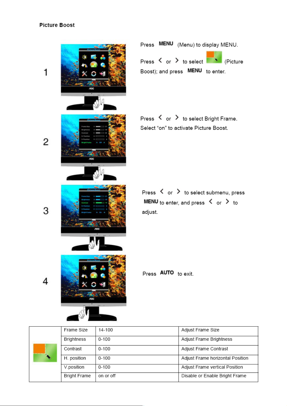
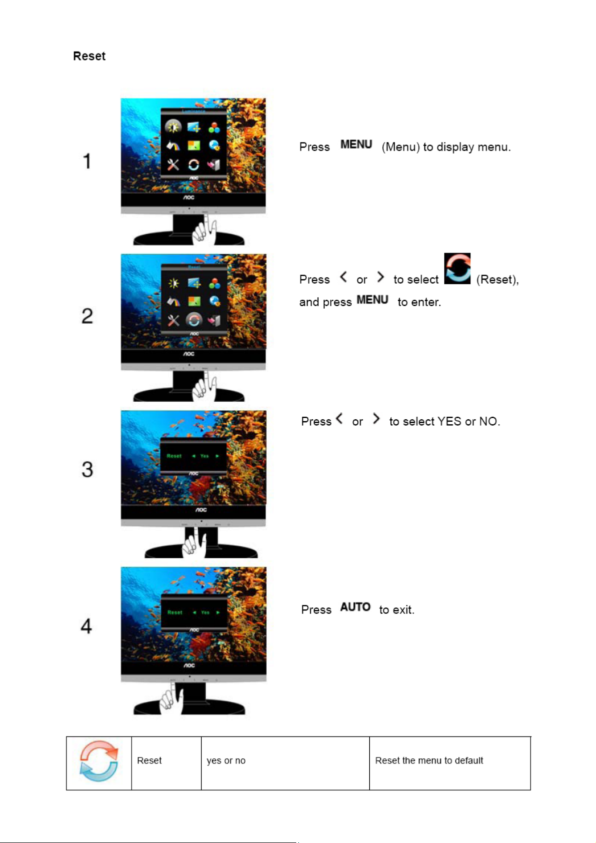
3. Operation Instructions
3.1 General Instructions
Press the power button to turn the monitor on or off. The other control knobs are located at front panel of the monitor.
By changing these settings, the picture can be adjusted to your personal preferences.
3.2 Control Buttons and Connections
Power: Press the Power button continuously to turn off the monitor.
Eco Mode / <
Press the Eco key continuously to select the Eco mode of brightness when there is no OSD (Eco mode hot key
may not be available in all models).
Volume/ >: When there is no OSD, press Volume (>) to active adjustment bar, press < or > to adjust volume.
Auto / Exit: When the OSD is closed, press Auto button will be auto configure hot key function.
1. Power 2. Analog (DB-15 VGA cable) 3. Audio
To protect equipment, always turn off the PC and LCD monitor before connecting.
1 Connect the power cable to the AC port on the back of the monitor.
2 Connect one end of the 15-pin D-Sub cable to the back of the monitor and connect the other end to the computer's
D-Sub port.
3 Connect the audio cable to audio in port on the back of the monitor.
6
Page 7

3.3 Adjusting the Picture
OSD Settings
Basic and simple instruction on the control keys.
1) Press the MENU-button to activate the OSD window.
2) Press < or > to navigate through the functions. Once the desired function is highlighted, press the MENU-button
to activate sub-menu . Once the desired function is highlighted, press MENU-button to activate it.
3) Press < or > to change the settings of the selected function. Press < or > to select another function in sub-menu .
Press AUTO to exit . If you want to adjust any other function, repeat steps 2-3.
4) OSD Lock Function: To lock the OSD, press and hold the MENU button while the monitor is off and then press
power button to turn the monitor on. To un-lock the OSD - press and hold the MENU button while the monitor is
off and then press power button to turn the monitor on.
Notes:
1) If the product has only one signal input, the item of "Input Select" is disable to adjust.
2) If the product screen size is 4:3 or input signal resolution is wide format, the item of "Image Ratio" is disable to
adjust.
3) One of DCR, Color Boost, and Picture Boost functions is active, the other two function is turned off accordingly.
7
Page 8
8
Page 9
9
Page 10

10
Page 11

11 12 13 14 15 16
Page 12

Page 13
Page 14

Page 15

Page 16
Page 17
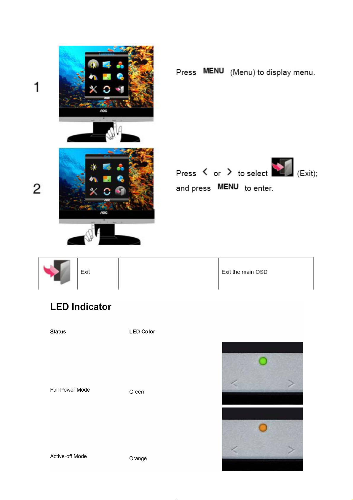
Exit
17
Page 18
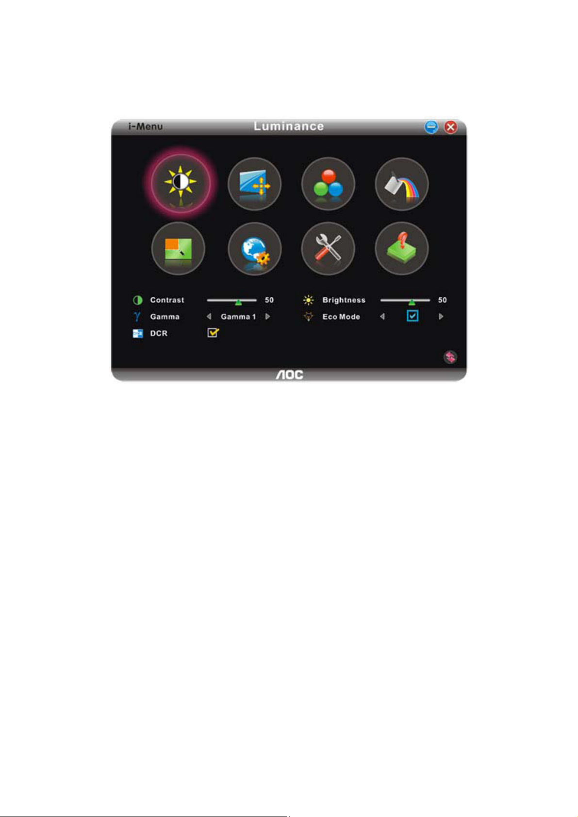
i - Menu
Welcome to “i-Menu” software by AOC. i-Menu makes it easy to adjust your monitor display setting by using on
screen menus instead of the OSD button on the monitor. To complete installation, please follow the installation
guide.
18
Page 19

4. Input / Output Specification
4.1 Input Signal Connector
D-Sub 15pin Connector
Pin Number Description Pin Number Description
1 Video-Red 9 +5V
2 Video-Green 10 Ground
3 Video-Blue 11 N.C.
4 N.C. 12 DDC-Serial data
5 Detect Cable 13 H-sync
6 GND-R 14 V-sync
7 GND-G 15 DDC-Serial clock
8 GND-B
4.2 Factory Preset Display Modes
Stand Resolution Horizontal Frequency(kHz) Vertical frequency(Hz)
VGA 640×480 @60Hz 31.469 59.940
VGA 640×480 @67Hz 35.000 66.667
VGA 640×480 @72Hz 37.861 72.809
VGA 640×480 @75Hz 37.500 75.000
Dos-mode 720×400 @70Hz 31.469 70.087
SVGA 800×600 @56Hz 35.156 56.250
SVGA 800×600 @60Hz 37.879 60.317
SVGA 800×600 @72Hz 48.077 72.188
SVGA 832×624 @75Hz 46.875 75.000
Mac-mode 832×624 @75Hz 49.725 74.500
XGA 1024×768 @60Hz 48.363 60.004
XGA 1024×768 @70Hz 56.476 70.069
XGA 1024×768 @72Hz 57.500 72.074
XGA 1024×768 @75Hz 60.023 75.029
XGA 1024×768 @75Hz 60.241 74.927
wXGA 1360×768 @60Hz 47.712 60.015
wXGA 1366×768 @60Hz 47.765 59.856
19
Page 20

4.3 Panel Specification
This specification applies to the 15.6 inch-wide Color a-Si TFT-LCD Module M156XW01.The display supports the
HD -1366(H) x 768(V) screen format and 16.7M colors (RGB 6-bits + Hi-FRC data). All input signals are LVDS
interface and this module doesn’t contain an inverter board for backlight.
4.3.1 General Feature
Items Unit Specifications
Screen Diagonal [mm] 15.6”
Active Area [mm] 344.232 (H) x 193.536 (V)
Pixels H x V 1366(x3) x 768
Pixel Pitch [um] 252 (per one triad) ×252
Pixel Arrangement R.G.B. Vertical Stripe
Display Mode TN Mode, Normally White
White Luminance (Center ) [cd/m2] 250 cd/m2 (Typ.)
Contrast Ratio 500 (Typ.)
Optical Response Time [msec] 8ms (Typ., on/off)
Nominal Input Voltage VDD [Volt] +5.0 V
Power Consumption (VDD line + CCFL line) [Watt] 13W (Typ.) (without inverter, all black pattern)
Weight [g] 1300 (Typ.)
Physical Size [mm] 363.8(W) X 215.9(H) X 14.3(D) Typ.
Electrical Interface One channel LVDS
Support Color 16.7M colors (RGB 6-bit + Hi-FRC )
Surface Treatment Anti-Glare, 3H
RoHS Compliance RoHS Compliance
TCO’03 Compliance TCO’03 Compliance
20
Page 21

4.3.2 Optical Characteristics
The optical characteristics are measured under stable conditions at 25℃:
21
Page 22

4.3.3 Electrical Characteristics
TFT LCD Module
Symbol Parameter Min Typ Max Unit Conditions
VDD Logic/LCD Drive Voltage 4.5 5.0 5.5 [Volt] +/-10%
IDD Input Current - 0.5 0.6 [A]
PDD VDD Power - 2.5 3.0 [Watt]
IRush Inrush Current - - 2.5 [A]
VDDrp
Allowable Logic/LCD
- - 300 [mV] p-p
Drive Ripple Voltage
VDD= 5.0V, All Black
Pattern At 60Hz
VDD= 5.0V, All Black
Pattern At 60Hz
VDD= 5.0V, All Black
Pattern At 60Hz
Backlight Unit
Parameter guideline for CCFL Inverter is under stable conditions at 25 (Room Temperature):
Parameter Min. Typ. Max. Unit
CCFL Standard Current (ISCFL) 7.0 7.5 8.0 [mA] rms
CCFL Operation Current (IRCFL) 3.0 7.5 8.0 [mA] rms
CCFL Frequency (FCFL) 40 43 60 [KHz]
CCFL Ignition Voltage (ViCFL, Ta= 0℃)
CCFL Ignition Voltage (ViCF, Ta= 25℃)
CCFL Operation Voltage (VCFL) -
CCFL Power Consumption (PCFL) - 10.5 - [Watt]
CCFL Life Time (LTCFL) 40,000 50,000 - [Hour]
1350 - - [Volt] rms
1050 - - [Volt] rms
660(@7.5mA)
- [Volt] rms
22
Page 23

(
)
(
)
5. Block Diagram
5.1 Main board
Flash ROM
SST25LF020A
U402
14.31818MHZ
(X401)
Scalar TSUM1PLR-LF
(Include MCU, ADC, OSD)
(U401)
D-Sub Connector
(CN101)
Panel Interface
(CN403)
Key Control
Interface
CN401
23
Page 24

5.2 Power board
AC input
EMI filter
Bridge rectifier
and Filter
Transformer
Rectifier
Diodes
Lamp
Start Circuit
CN902
5V
PWM Control IC
Feedback circuit
ON/OFF
DIM
OSC and
Output Circuit
Feedback
Circuit
DC Convert
Circuit
Over Voltage
protect
MOSFET
PWM Control IC
12V
ON/OFF Control
24
Page 25

6. Schematic
6.1 Main Board
715G2904 2 2
ESD_VCC
CMVCC1
VCC3. 3
CMVCC
ESD_VC C
DSUB_5V
DSUB_5V
VCC3.3
XGA/SXGA
DSUB_5V
ESD_VC C
VCC3.3
02.Input
VCC1.8
VCC1.8
VCC3.3
CMVCC
CMVCC1
DET_CABLE
on_BACKLI GHT
Adj_BACKLI GHT
DSUB_R+
DSUB_R-
DSUB_G+
DSUB_G-
DSUB_SOG
DSUB_B+
DSUB_B-
DSUB_H
DSUB_V
DDC1_SDA
DDC1_SCL
Mut e
Volume#
PANEL_ID#DSUB_5V
VCTRL
DSUB_R+
DSUB_RDSUB_G+
DSUB_GDSUB_SOG
DSUB_B+
DSUB_BDSUB_H
DSUB_V
DDC1_SDA
DDC1_SCL
DET_CABLE
on_BACKLI GHT
Mut e
Volume#
PANEL_I D#
Adj_BACKLI GHT
VCTRL
VCC1.8
VCC3. 3
CMVCC
CMVCC1
PA[0. .1]
PA[4..9]
PB[0. .9]
PPWR _ON#
LVDS OUTPUT
VCC1. 8
VCC3. 3
CMVCC
CMVCC1
PA[0. .1]
PA[4. .9]
PB[0. .9]
PA[0.. 1]
CMVCC
PA[4. .9]
PB[0. .9]
PPWR _ON#
CMVCC
ESD_VC C
05.Pow e r
03.Scala r
T P V ( Top Victory Elec tronics Co . , Lt d. )
絬 隔 瓜 絪 腹
Key Component
Date
G2904-1-X-X-11-080416
01.Top
25
04.Output
OEM MODEL Size
TPV MOD E L
PCB N AME
Sheet
715G2904-1
of
37Wednes day , April 16, 2008
Rev
称爹
<
A
E
称爹
>
Page 26

H_Sync
R101 0R05 1/ 10W 5%
V_Sy nc
VCC3.3
R120
R121
10K 1/16W 5%
DDC1_SCL5
DDC1_SDA5
DDC1_SCL
DDC1_SDA
GND POWER
DSUB_SDA
DSUB_SCL
10K 1/16W 5%
R110
100R 1/16W 5%
R113
100R 1/16W 5%
DGND
U103
1
I/O1
I/O4
2
GND
VDD
3 4
I/O2 I/O3
AZC099-04S
DSUB_SCL
DSUB_SDA
6
5
H_Sync
V_Sy nc
15
14
13
12
11
ESD_VCC
C115
NC
R105
2K2 1/16W 5%
CN101
10
5
9
4
8
3
7
2
6
1
DB15
17 16
ESD_VCC 5
DSUB_5V
VGA_BVGA_B+
VGA_GVGA_G+
VGA_RVGA_R+
R106
2K2 1/16W 5%
ZD103
UDZSNP5.6B
C102
22pF
VGA_PLUG
1 2
R102 100R 1/ 16W 5%
R103 100R 1/ 16W 5%
C103
22pF
DSUB_5V
ZD104
UDZSNP5.6B
1 2
DSUB_5V 5
DSUB_H 5
DSUB_V 5
VGA_B+
VGA_B-
VGA_G+
VGA_G-
VGA_R+
VGA_R-
FB102
1 2
BEAD
FB103
1 2
BEAD
FB101
1 2
BEAD
R107
75R 1/16W 5%
R112
75R 1/16W 5%
R116
75R 1/16W 5%
R104
100R 1/16W 5%
C104
5pF/50V
R108
100R 1/16W 5%
R109
390 OHM 1/16W
R111
100R 1/16W 5%
C108
5pF/50V
R114
100R 1/16W 5%
R115
100R 1/16W 5%
C111
5pF/50V
R117
100R 1/16W 5%
C101
0.047uF
C105
0.047uF
C106
0.047uF
C107
0.047uF
C109
0.047uF
C110
0.047uF
C113
0.047uF
DSUB_B+ 5
DSUB_B- 5
DSUB_SOG 5
DSUB_G+ 5
DSUB_G- 5
DSUB_R+ 5
DSUB_R- 5
VGA_G+
VGA_R+
U102
1
I/O1
I/O4
2
GND
VDD
3 4
I/O2 I/O3
AZC099-04S
VCC3.3
VGA_B+
ESD_VCC
C114
NC
T P V ( Top Victory Electronics Co . , Ltd. )
絬 隔 瓜 絪 腹
Key Component
G2904-1-X-X-11-080416
02.Input
Date
VGA_PLUG
OEM MO DE L Size
TPV MO DE L
PCB NAME
Sheet
715G2904-1
of
47Wednesday , April 16, 2008
6
5
R118
1K 1/16W 5%
VCC3.3 7
DET_CABLE 5
Rev
称爹
B
E
称爹
>
<
26
Page 27

VDDC
VDDP
AVDD
VCC3.3
CMVCC17
VCC3.3
C408
0.22uF16V
R408
10K 1/16W 5%
CMVCC1
C410
10uF/50V
+
U402
1
CE#
2
SO
WP
3
WP#
4 5
VSS SI
SST25VF010A-33-4C- SAE
R417
10K 1/16W 5%
HOLD#
U401
0.1uF/ 16V
R401
R402
C401
13
RIN0P
12
RIN0M
10
GIN0P
9
GIN0M
11
SOGIN0
8
BIN0P
7
BIN0M
16
HSYNC0
17
VSYNC 0
18
DDCA_SD A/RS232_TX
19
DDCA_SCL/rs232_RX
4
REXT
15
REFP
14
REFM
21
SDO
22
SCZ
23
SCK
24
SDI
28
GPIO_P27/PW M1
54
RST
1
XIN
2
XOU T
31
MODE [0]
32
MODE [1]
DSUB_R+3
DSUB_R-3
DSUB_G+3
DSUB_G-3
DSUB_SOG3
DSUB_B+3
DSUB_B-3
DSUB_H3
DSUB_V3
DDC1_SDA3
DDC1_SCL3
AVDD
R403 390 OHM 1/16 W
8
VDD
7
6
SCK
C411 22pF
C412 22pF
R456 100R 1/16W 5%
R457 100R 1/16W 5%
R405 100R 1/16W 5%
0R05 1/16W
X401
14.31818MHz
0R05 1/16W
1 2
6
51
VDDP
AVDD_ADC
LVDS
GND
GND
GND
5
29573
TSUM1PLR-LF
30
53
VCTRL
VDDC
VDDC
LVA3P
LVA3M
LVA2P
LVA2M
LVA1P
LVA1M
LVA0P
LVA0M
LVB3P
LVB3M
LVBCKP
LVBCKM
LVB2P
LVB2M
LVB1P
LVB1M
LVB0P
LVB0M
GPIO_P15/P WM0
PWM2/GPIO_P24
GPIO_P12
PWM1/GPIO_P25
RSTN
GPIO_P00/SAR 1
GPIO_P01/SAR 2
GPIO_P06
GPIO_P07
PWM0/GPIO_P26
GPIO_P13
GPIO_P14
GPIO_P10/I2C_MCL
GPIO_P11/I2C_MDA
52
PA0
33
PA1
34
35
PA4
36
PA5
37
PA6
38
PA7
39
PA8
40
PA9
41
PB0
42
PB1
PB2
43
44
PB3
45
PB4
46
PB5
47
PB6
48
PB7
PB8
49
50
PB9
20
R424 NC
27
55
56
58
R411 100R 1/16W 5%
59
R412 100R 1/16W 5%
60
R414 470R 1/16W 5%
61
R410 620R OHM 1/16W 5%
62
R418 100R 1/16W 5%
63
R419 100R 1/16W 5%
64
26
R413 100R 1/16W 5%
25
PA[0..1]
PA[4..9]
PB[0..9]
KEY2
KEY1
LED_GRN/BLUE
LED_ORAN GE
R425
NC
VCTRL 7
PA[0.. 1] 5
PA[4.. 9] 5
PB[0.. 9] 5
C418
NC
on_BACKLIGH T 7
adj_BACKLIGH T 7
Volume# 7
Mute 7
PPWR_ON # 6
DET_CABLE 4
EE_WP
R426 NC
R452 NC
R420 10 0R 1/16W 5%
R451 NC
MSCL
MSDA
VCC3.37
VCC1.87
MSDA
POWER_KEY #
MSCL
VDDP
VCC1.8
VDDC
PANEL_ID # 7
R455
R453
R454
NC
NC
NC
FB401
300OHM
C403
0.1uF/16V
C406
0.1uF/16V
EE_WP
AVDD
C404
0.1uF/ 16V
C407
0.1uF/ 16V
CMVCC
R406
10K 1/16W 5%
U403
8
VCC
7
WC
6
SCL
NC / M24C04-WMN6TP
CMVCC 7
R409
20K OHM 1/16W
C409 0.1uF /16V
1
NC
2
E1
3
E2
45
VSSSDA
VCC3.3
C429
NC
CN401
CONN
VCC3.3
R421
10K 1/16W 5%
1
2
3
4
5
6
R427
3.9K OHM 1/ 16W
C413
0.1uF/ 16V
C414
0.1uF/ 16V
R428
3.9K OHM 1/ 16W
C415
0.1uF/ 16V
C416
0.1uF/ 16V
R404
10K 1/16W 5%
C417
0.1uF/ 16V
KEY1
KEY2
POWER_KEY#
LED_GRN/BLUE
LED_ORANGE
R407
10K 1/16W 5%
POWER_KEY#
LED_ORAN GE
LED_GRN/BLUE
R429 NC
R430 NC
R431 NC
R432 NC
KEY_LEF T
KEY_RI GHT
KEY_AUTO
CN402
1
2
3
4
5
6
7
8
NC \ CONN
T P V ( Top Victory Electronics Co . , Ltd. )
G2904-1-X-X-11-080416
絬 隔 瓜 絪 腹
Key Component
03.Scalar
Date
OEM MOD EL Size
TPV MOD EL
715G2904-1
PCB NAME
57Wednesday , April 16, 2008
Sheet
of
C
E
Rev
<
称爹
>
称爹
27
Page 28

PANEL_VCC
CN403
PA[0. .1]5
PA[4. .9]5
PPWR_ON#5
PA[0..1]
PA[4..9]
R435
4K7 1/16W 5%
PPWR_ON#
PB[0..9]5
PA0
PA1
PA4
PA5 PB6
PA6
PA7
PA8
PA9
R433
10K 1/16W 5%
R436
100K 1/16W 5%
Q404
PMBS3906
PB[0..9]
C419
0.1uF/16V
CMVCC
Q405
AO3401
PB0
PB1
PB2
PB3
PB4
PB5
PB7
PB8
PB9
CMVCC 7
FB402
120OHM
PANEL_VCC
C421
+
100uF25V
330 OHM 1/4W
3
D
1
G
AO3401L
R434
2
S
C420
0.1uF/16V
PA0
PA1
PB2
PB3
PA4
PA5
PA6
PA7
PA8
PA9
PB0
PB1
PB2
PB3
PB4
PB5
PB6
PB7
PB8
PB9
10
11
12
13
14
15
16
17
18
19
20
21
22
23
24
25
26
27
28
29
30
1
2
3
4
5
6
7
8
9
CONN
T P V ( Top Victory Electronics Co . , Ltd. )
絬 隔 瓜 絪 腹
Key Component
Date
G2904-1-X-X-11-080416
04.Output
28
OEM MODEL Size
TPV MODEL
PCB N AME
Sheet
715G2904-1
67Wednesday , April 16, 2008
of
Rev
称爹
<
A
E
称爹
>
Page 29

ESD_VCC 2
DSUB_5V
CN404
CONN
1
2
3
4
5
6
7
8
9
CMVCC5, 6
CMVCC
CMVCC
BKLT-VBRI
BKLT-EN
C_PANEL_INDEX
Volume
Mut e
CMVCC
SM340A
D402
R450 NC
R458
NC
NC(R0402)
2
3
PANEL_ID# 5
CMVCC1
DSUB_5V 2
1
D401
BAV99
R449
NC
CMVCC1 5
Mut e 5
BKLT-EN
C425
NC
VCC3. 3
R437
10K 1/16W 5%
Q406
2N3904S-R TK/PS
VCC3.3
R440
4K7 1/16W 5%
R439
10K 1/16W 5%
on_BACKLI GHT 5
VCC3.3
C432
0.1uF/ 16V
VCC1.8
+
C423
100uF25V
VCC1.8 5
Q410
KN2907AS
Q409
VCTRL5
KN2907AS
BKLT-VBRI
VCC3.3
R441
1K 1/16W 5%
100R 1/16 W 5%
R442
adj_BACKLI GHT 5
Volume
VCC3.3
R446
10K 1/16W 5%
Q408
2N3904S-R TK/PS
VCC3.3
R448
4K7 1/16W 5%
R447
10K 1/16W 5%
Volume# 5
CMVCC1
T P V ( Top Victory Electronics Co . , Ltd. )
絬 隔 瓜 絪 腹
Key Component
G2904-1-X-X-11-080416
05.Power
Date
+
C426
100uF25V
MVC C
C428
0.1uF/ 16V
FB403 NC
VCC3.3
3
VIN
2
VOUT
ADJ(GND)
U404
AP1117D33LA
1
+
C422
0.1uF/16V
OEM MODEL Size
TPV MO D EL
Sheet
715G2904-1
77Wednesd ay , April 16, 2008
of
PCB NAME
C427
100uF25V
VCC3.3 4, 5
Rev
称爹
B
E
<
称爹
>
29
Page 30

6.2 Power Board
715G2852 2
1
!
+
R900
680K OHM 1/4W
!
t
KBP208G
C902
1000pF
!
NR901
NTCR
2
BD901
!
!
0.22uF/ 275V
680K OHM 1/4W
CN901
SOCKET
87G 501 32 S
-
4
C904
0.22uF/ 275V
2
3
1
4
C908
R902
!
VAR901
Varistor
N.C
3
!
C901
1000pF
L901
30mH
680K OHM 1/4W
!
12
!
3
!
!
!
R901
!
+
R915
100K OHM 1% 1/8W
!
F901
FUSE 3. 15A 250V
C907
100uF450V
C938
NC
C911
0.1uF
0.01uF
C928
ZD906
RLZ22B
1 2
IC901
RT4NC
3
VCC
2
COMP
1
GND
LD7552BPS
GND1
GND
1
2
HS2
HEAT SINK(D 906_Q90G6263-3)
1
2
HS3
HEAT SIN K(Q901_Q90G6263-3)
1
2
R904
300K OHM 1/4W
R932
300K OHM 1/4W
R933
300K OHM 1/4W
5
6
CS
7
VCC
8
OUT
R905
NC
R906
NC
+
R907
NC
D903
LL4148
R910
10R 1/4W
ZD905
RLZ18B
R912
220 OHM 1/4W
C909
470pF/25V
HS5
SHIELD (H85G0002-1)
1
2
D901
FR103
C903
22uF/50V
1 2
C906
1500pF2KV
R938
10K 1/8W
R908
100KOHM + -5% 2WS
D900
FR107
R909
5.1 OHM 1/4W
!
Q901
2SK2645-54MR
12
FB901
BEAD
R914
0.47 OHM +-5% 2WS
4
5
6
2
1
!
C900
3300pF 250V
!
T901
POWER X'FMR
43
9
10
7
8
11
12
12
IC902
PC123X2YFZ OF
IC903
AZ431AZ-AE1
R918
100 OHM 1/4W
R919
100 OHM 1/4W
R920
100 OHM 1/4W
R921
100 OHM 1/4W
R922
100 OHM 1/4W
R923100 OHM 1/4W
R961 100 O HM 1/4W
R962 100 O HM 1/4W
R935 100 O HM 1/4W
C924
0.1uF
C912
0.001uF
2
D906
FCH10U10
R925
1K 1/8W
R926
1K 1/10W 1%
C925
NC
3
C929
0.001uF
680uF/25V
1
D907 31DQ06FC 3
D905 31DQ06FC 3
L904
1.0uH
+
+
C917
C910
0.001uF
絬 隔 瓜 絪 腹
Key Component
C918
680uF/25V
L905
1.0uH
+
C921
470uF/16V
+
C939
820uF25V
+
C940
1000uF25V
T P V ( Top Victory Electronics Co . , Ltd. )
G2852-2-X-X-33-090515
2.POWER
Date
R948
56 OHM +-5% 2WS
Q904
PMBS3904
L903
1.0uH
R924
150R 1/8W
ZD922
RLZ5.1B
D916
LL4148
1K 1/10W 1%
2.43K OHM 1% 1/10W
+
R942
R930
C922
470UF/ 25V
RLZ5.6B
1 2
ZD923
1 2
R947
470R 1/8W
R952
1K 1/8W
ZD921
RLZ13B
1 2
R927
3.6K OHM 1% 1/10W
D915
LL4148
ON/OF F
OEM MOD EL
TPV MO DEL
PCB NAME
715G2852-2
24Friday , May 15, 20 09
Sheet
MUTE
DIM
of
VOL
+5V
R940
33K 1/10W
R946
150 OHM 2W
Q903
PMBS3904
C932
0.001uF
C915
470uF/16V
C931
0.1uF
+
ZD902
RLZ13B
1 2
R943
470R 1/8W
R939
1K 1/8W
F902
NC
F904
0R05 1/4W
F903
NC
F905
0 OHM 1/4W
Size
Rev
称爹
C930
0.1uF
10
1
2
3
4
5
6
7
8
9
+12V
+5V1
+5V
CN902
CONN
Custom
1
ODM MODEL
30
Page 31

1
2
D801
BAV99
D802
BAV99
CONN
CN801
2
1
1
2
CONN
CN802
2
1
ON/OFF
C839
1500PF/50V
R855
+12V
DIM
F801
0 OHM 1/4W
Q805
PDTC144WK
C807
0.1uF/25V
R804
100R 1/8W
Q808
PDTA144WK
C825
0.1uF/25V
PMBS3904
Q804
PMBS3906
C802
Q801
23
1
Q811
PMBS3904
D810
NC
R839
22R 1/8W
D811
NC
470UF/25V
C824
+
0.1uF
Q802
AM9945N-T1-PF
1
S
D
2
G
D
3
S
D
4
G
D
15R 1/4W
R856
15R 1/4W
8
C838
7
1500PF/50V
6
5
POWER X'FMR
6
3
4
T801
7
C801
30pF/3KV
81
C803
30pF/3KV
D807
LL4148
D805
LL4148
C819
0.0022uF
C823
0.0022uF
R817
10K 1/10W 1%
R828
10K 1/10W 1%
R821
1K 1/8W
3
R801
1K5 1/10W 1%
R822
1K 1/8W
3
R814
1K5 1/10W 1%
D817
LL4148
6K8 1/10W
10K 1/10W 1%
R827
1K 1/10W 1%
R851
R830
NC
R820
R802
6K8 1/10W
C822
1uF/25V
D812
LL4148
10K 1/10W 1%
Q806
PMBS3904
C842
0.01uF
R863
C835
NC
R832
10K 1/10W 1%
R831
1K 1/8W
R823
0R05 1/10W 5%
C821
0.1uF/25V
51K OHM 1% 1/8W
R810
C820
220pF50V
PMBS3906
R865
NC
Q812
1
R853
68K 1/10W
R861
NC
Q807
N.C
R850
23
22R 1/8W
R841
68K OHM 1% 1/10W
R829
22R 1/8W
R825
22R 1/8W
R837
47K 1/8W
R807
R824
1K 1/10W 1%
10K 1/10W 1%
R808
10K 1/10W 1%
C845
2.2uF/16V
R862
1M 1/10W 5%
R803
680K 1/10W
D814
LL4148
C846
NC
C834
0.01uF/25V
G2852-2-X-X-33-090515
3.INVER TER
D806
LL4148
R835
NC
R818
1K 1/10W 1%
Q809
RK7002
T P V ( Top Victory Electronics Co . , Ltd. )
絬 隔 瓜 絪 腹
Key Component
Date
OEM MOD EL
TPV MOD EL
PCB NAME
Sheet
715G2852-2
34Friday , May 15, 2009
of
Size
Custom
Rev
1
ODM MODEL
称爹
IC801 AZ7500F MTR
1
1IN+
2
1IN-
3
FEEDBACK
4
DTC
5
CT
6
RT
7
GND
8
C1
R864
NC
C817
NC
OUTPUT CTRL
R854
NC
16
2IN+
15
2IN-
14
REF
13
12
VCC
11
C2
10
E2
9
E1
R826
1K 1/8W
31
Page 32

CN601
PHONEJAC K
+5V1
C602 0. 47uF/ 16V
R602
10K 1/10W 5%
VOL
R603
10K 1/10W 5%
MUTE
Lin
4
5
3
Rin ROUT+
2
1
R608
1R 1/8W
R604 10K 1/10W 5%
R605 10K 1/10W 5%
100pF
C610
R606
R607
5K6 1/10W
C611 100pF
C609
1uF/25V
C601 0.47uF/16V
C606 0.47uF/16V
5K6 1/10W
R601
10K 1/10W 5%
8
7
6
5
4
3
2
1
C608
1uF/25V
C613
0.1uF/16V
C612
0.1uF/16V
IC with Heat-sink(90G6295-3)
C604
100uF/25V
IC601
SE/BTL
VOLUME
LINGND
GND
RINBYPASS
SHUTDOWN
APA2069JITUL
+
LOUT-
VDD
LOUT+
GND
GND
ROUT+
VDD
ROUT-
C603 0. 47uF/ 16V
9
10
11
12
13
14
15
16
LOUT-
LOUT+
ROUT-
CONN
4
3
2
1
CN602
T P V ( Top Victory Electronics Co . , Ltd. )
絬 隔 瓜 絪 腹
Key Component
Date
G2852-2-X-X-33-090515
4.AUDIO
32
FB602
1 2
BEAD
OEM MOD E L
TPV MOD E L
PCB N AME
Sheet
715G2852-2
44Friday , May 15, 2009
of
Size
Rev
称爹
A
1
OD M MO D EL
Page 33

6.3 Key Board
715G2835 2
CN001
LBADC1
1
LBADC2
2
DC_POWERON
3
LED_GRN#
4
LED_Y ELLOW#
5
6
CONN
SGND
C001
NC/0.001uF
C002
NC/0.001uF
LED_Y ELLOW#
1
C003
NC/0.001uF
LED_GRN#
3
D001
LED
2
C004
NC/0.001uF
C005
NC/ 0.001uF
R002 2.0 KOHM +-1% 1/4W
R003 0 OHM +-1% 1/10W
R004 2.0 KOHM +-1% 1/4W
R005 1 KOHM +-1% 1/10W
SW005
ZD002NC/UDZS5.6B
C007NC/0.1uF
3 4
OK
21
5
SW
C009NC/0.1uF
SW004
ZD005NC/UDZS5.6B
3 4
UP
21
5
SW
C010NC/0.1uF
ZD003NC/UDZS5.6B
SW003
3 4
POWER
21
5
SW
C008NC/0.1uF
SW002
ZD004NC/UDZS5.6B
3 4
SGNDSGND SGNDSGNDSGNDSGNDSGN DSGND
DOWN
21
5
SW
C006NC/0.1uF
SW001
ZD001NC/UDZS5.6B
3 4
SGND
MENU
21
5
SW
SGND
(Power)
GND
CONNECTOR
LED(MENU)
(OK)(DOWN)(UP)
T P V ( Top Victory Electronics Co . , Ltd. )
絬 隔 瓜 絪 腹
Key Component
G2835-2
Date
OEM MODEL
TPV MO D EL
PCB NAME
Sheet
715G2835-2key
of
22
Size
Rev
称爹
B
A
33
Page 34

7. PCB Layout
7.1 Main Board
715G2904 2 2
34
Page 35

35
Page 36

7.2 Power Board
715G2852 2
36
Page 37

7.3 Key Board
715G2835 2
37
Page 38

8. Maintainability
8.1 Equipments and Tools Requirement
1. Voltmeter.
2. Oscilloscope.
3. Pattern Generator.
4. DDC Tool with an IBM Compatible Computer.
5. Alignment Tool.
6. LCD Color Analyzer.
7. Service Manual.
8. User Manual.
38
Page 39

G
G
8.2 Trouble Shooting
No Power
No power
Check power cable is
tightened?
N
Re-plug the power cable
O
Check Power
“On/Off” is “On”?
NG
Turn on the Power “On/Off” switch
O
Check the LED
indicate is OK?
N
Check the AC power
O
Replace the converter board
NG
Replace main board and check connections
NG
Replace key board and check connections
39
Page 40

No Video (Power LED Green)
No Video (Power LED Green)
Press the power
button is OK?
NG
Replace the main board
Replace the converter
board
OK
The end
Replace the main
board and connection
OK
The end
NG
Check the LVDS/FFC
cable or panel
OK
Replace the LVDS/FFC
cable or panel
NG
Replace the key board
40
Page 41

q
y
DIM
DIM (image overlap, focus or flicker)
Reset in factory mode
NG
OK
The end
Set to the optimal
frequency, select the
recommended fre
uenc
OK
The end
NG
Readjust the phase and pixel
clock in the user mode
OK
The end
NG
Pull out signal cable and
check “Self Test Feature
Check” is ok?
OK
Check the signal cable
and the PC
NG
NG
Replace the main board
OK
The end
NG
Replace the panel
OK
41
Page 42

g
Color is not optimal
Color is not optimal
Miss color
Replace the signal cable
NG
OK
The end
In the user mode, set the” color
settin
Pull out the signal cable
and check the screen
color display is normal?
OK
Color shift
Reset the factory mode
NG
s” until customer satisfy
NG
NG
Replace the signal cable or PC
Replace the main board
42
Page 43

9. White- Balance, Luminance Adjustment
Approximately 30 minutes should be allowed for warm up before proceeding white balance adjustment.
How to setting MEM channel you can reference to chroma 7120 user guide or simple use “SC” key and “NEXT” Key
to modify xyY value and use “ID” key to modify the TEXT description Following is the procedure to do white-balance
adjust .
2. Setting the color temp. you want
A. MEM.CHANNEL 3 6500K (Warm color):
2
2
2
Warm color temp. parameter is x = 313 ±30, y = 329 ±30, Y>150cd/m
B. MEM.CHANNEL 4 7300K (Normal color):
Normal color temp. parameter is x = 302 ±30, y = 318 ±30, Y>150cd/m
C. MEM.CHANNEL 9 9300K (Cool color):
Cool color temp. parameter is x = 283 ±30, y = 297 ±30, Y>130cd/m
D. MEM.CHANNEL 10 (sRGB color):
sRGB color temp. parameter is x = 313 ±30, y = 329 ±30, Y>150cd/m2
3. Enter into the factory mode:
Press the MENU button, pull out the power cord, and then plug the power cord. Then the factory OSD will be at the
left top of the panel.
4. Bias adjustment:
Set the Contrast
to 50; Adjust the Brightness to 80.
5. Gain adjustment:
Move cursor to “-F-” and press MENU key
A. Adjust Warm (6500K) color-temperature
1. Switch the chroma-7120 to RGB-Mode (with press “MODE” button)
2. Switch the MEM.channel to Channel 3 (with up or down arrow on chroma 7120)
3. The LCD-indicator on chroma 7120 will show x = 313 ±30, y = 329 ±30, Y>150cd/m
2
4. Adjust the RED on factory window until chroma 7120 indicator reached the value R=100
5. Adjust the GREEN on factory window until chroma 7120 indicator reachedthe value G=100
6. Adjust the BLUE on factory window until chroma 7120 indicator reached the value B=100
7. Repeat above procedure (item 4, 5, 6) until chroma 7120 RGB value meet the tolerance =100±2
43
Page 44

B. Adjust Normal (7300K) color-temperature
1. Switch the chroma-7120 to RGB-Mode (with press “MODE” button)
2. Switch the MEM.channel to Channel 4(with up or down arrow on chroma 7120)
3. The LCD-indicator on chroma 7120 will show x = 302 ±30, y = 318 ±30, Y>150cd/m
4. Adjust the RED on factory window until chroma 7120 indicator reached the value R=100
5. Adjust the GREEN on factory window until chroma 7120 indicator reachedthe value G=100
6. Adjust the BLUE on factory window until chroma 7120 indicator reached the value B=100
7. Repeat above procedure (item 4, 5, 6) until chroma 7120 RGB value meet the tolerance =100±2
C. Adjust Cool (9300K) color-temperature
1. Switch the Chroma-7120 to RGB-Mode (with press “MODE” button)
2. Switch the MEM. Channel to Channel 9 (with up or down arrow on chroma 7120)
3. The LCD-indicator on chroma 7120 will show x = 283 ±30, y = 297 ±30, Y>130cd/m
4. Adjust the RED on factory window until chroma 7120 indicator reached the value R=100
5. Adjust the GREEN on factory window until chroma 7120 indicator reached the value G=100
2
2
6. Adjust the BLUE on factory window until chroma 7120 indicator reached the value B=100
7. Repeat above procedure (item 4, 5, 6) until chroma 7120 RGB value meet the tolerance =100±2
D. Adjust sRGB color-temperature
1. Switch the chroma-7120 to RGB-Mode (with press “MODE” button)
2. Switch the MEM.channel to Channel 10 (with up or down arrow on chroma 7120)
3. The LCD-indicator on chroma 7120 will show x = 313 ±30, y = 329 ±30, Y>150cd/m
2
4. Adjust the RED on factory window until chroma 7120 indicator reached the value R=100
5. Adjust the GREEN on factory window until chroma 7120 indicator reachedthe value G=100
6. Adjust the BLUE of on factory window until chroma 7120 indicator reached the value B=100
7. Repeat above procedure (item 4, 5, 6) until chroma 7120 RGB value meet the tolerance =100±2
E. Turn the Power-button off to quit from factory mode.
44
Page 45

10. Monitor Exploded View
45
Page 46

No. Description
1 BEZEL
2 LENS
3 KEY BUTTON
4 KEY BOARD
5 PANEL
6 POWER BOARD
7 MAIN BOARD
9 MAIN FRAME
10 REAR COVER
11 HINGE S1 0M1G1030 6120 SCREW M3X6(FOR PB/MAINFRAME)
12 STAND TOP S2 0M1G1030 6120 SCREW M3X6(FOR MB/MAINFRAME)
13 STAND S3 0M1G 130 5120 SCREW(FOR MAINFRAME/PANEL)
14 BASE S4 AM1G1740 10 47 CR3 SCREW(FOR HINGE/MAINFRAME)
15 FOOT S5 AM1G1740 12225 CR3 SCREW(FOR HINGE/STAND TOP)
No. Part No. Description
46
Page 47

11. BOM List
Note: The parts information listed below are for reference only, and are subject to change without notice. Please go to
http://cs.tpv.com.cn/hello1.asp
for the latest information.
T69AM5NCYJRD9N
Location Part No. Description Remark
040G 581909 1A PROTECT LABEL
045G 77500 BARCODE RIBBON
045G 77501 BARCODE RIBBON
050G 600 3 HANDLE2
050G 600 4 HANDLE 1
052G 1185 MIDDLE TAPE (Y1200141)
052G 1185 1 BIG TAPE(Y1200141)
052G 1211 A CONDUCTIVE TAPE 55MM *45MM *0.08MM
052G 2191 A PAPER TAPE
052G6019 1 INSULATING TAPE
E07801 078G 322 9A G SPK 8 OHM 1.5W 43X18MM 145 200 NEO 2nd source
E07801 078G 322 9A K SPK 8OHM 1.5W 43X18 145 200MM KUAIDA
E07801 078G 322 9A Y SPK 8OHM 1.5W 145 200MM 43X18MM SUNLINK 2nd source
089G 17356X554 AUDIO CABLE
E08902 089G 725CAA DB D-SUB CABLE
E08902 089G 725GAA DB D-SUB CABLE 2nd source
E08902 089G 725HAA DB D-SUB CABLE 2nd source
E08901 089G404A15N IS AC POWER CORD 1500MM EUROPE REG.
E08901 089G404A15N YH AC POWER CORD 1500MM EUROPE REG. 2nd source
095G8014 6WH09 WIRE HARNESS 6P(PH)-6P(PH)
E09501 095G8018 3LH60 LVDS CABLE 30P-14P 140MM
E09501 095G8018 3XH60 HARNESS 30P-14P 140MM 2nd source
0M1G 130 5120 SCREW
0M1G1030 6120 SCREW M3X6
705GQ834319 16" LCD ASS'Y
AM1G1740 10 47 CR3 SCREW
Q12G6600 6 FOOT
Q34G0297AED 1B0100 STAND TOP
Q34G0298AED 1B0120 STAND
Q34G0299AED 1B0130 BASE8S2
M037 Q37G0067012CKD HINGE
M037 SQ37G0067012CKD HINGE ASS'Y 2nd source
015F0067210 SUPPORT
015F0067020 ACTIVE PLATE
004F0610051 01 WASHER
004F061210T 01 METAL WASHERS12.0*4.72*1.0T
47
Page 48

004F061210M 00 METAL WASHERS12.0*6.03*4.70H
004F0612052 00 METAL WASHER
028F0817070 SHAFT
0M1F3050106 SCREW
002F0605100 SCREW NUTS M6.0*P1.0
E750 750GLU156W0112N000 PANEL M156XW01 V000 SZ AUO
E750 750GLU156W0115N000 PANEL M156XW01 V000 DG AUO 2nd source
E750 750GLU156W0122N000 PANLE M156XW01 V00A SZ AUO 2nd source
E750 750GLU156W0125N000 PANEL M156XW01 V00A DG AUO 2nd source
756GQ9CB AA208 00 MAIN BOARD-CBPC9M5A4QSC
U402 056G1133 81 SST25LF020A-33-4C-SAE
SMTC9-U402 100GAMA6000YT1 MCU ASS'Y-056G1133 81
AM1G1740 12225 CR3 SCREW
040G 45762412B CBPC LABEL
CN401 033G3802 6 WAFER
CN404 033G3802 9 WAFER 9P RIGHT ANELE PITCH
CN403 033G804314C H HR WAFER 2*7P 2.0PICTH
CN101 088G 35315F HD D-SUB CONN F ATTACHED SCREW
CN101 088G 35315F XH D-SUB 15PIN VERTICAL CONN WITH SCREW
X401 093G 22 53 J 14.31818MHZ/32PF/49US
X401 093G 22 53 YC CRYSTAL 14.31818MHZ/32PF 49U/S YC
709G2904 QM002 CONSUMPTIVE ASS'Y
C410 067G 3151007KB EC 10UF M 50V 5*11
C421 067G 3151014KB EC 100UF M 25V 6.3*11
C427 067G 3151014KB EC 100UF M 25V 6.3*11
C426 067G 3151014KB EC 100UF M 25V 6.3*11
C423 067G 3151014KB EC 100UF M 25V 6.3*11
709G2904 QA001 CONSUMPTIVE ASS'Y
U401 056G 562702 IC TSUM1PLR-LF LQPF-64 MSTAR
U404 056G 563 52 IC AP1117D33G-13 TO252-3L DIODES
U404 056G 563515 IC AZ1117D-3.3TRG1 1A/3.3V TO-252
U404 056G 563916 IC LD1117DT33TR DPAK
U103 056G 662 13 IC AZC099-04S SOT23-6L
U102 056G 662 13 IC AZC099-04S SOT23-6L
U402 056G1133 81 SST25LF020A-33-4C-SAE
Q404 057G 417 6 PMBS3906/PHILIPS-SMT(06)
Q406 057G 417 12 T KEC 2N3904S-RTK/PS
Q408 057G 417 12 T KEC 2N3904S-RTK/PS
Q409 057G 417 22 T TRA KN2907AS -60V/-0.6A SOT-23
Q410 057G 417 22 T TRA KN2907AS -60V/-0.6A SOT-23
48
Page 49

Q404 057G 417517 TRA LMBT3906LT1G -200MA/-40V SOT-23 LRC
Q406 057G 417518 TRA LMBT3904LT1G 200MA/40V SOT-23 LRC
Q401 057G 763 1 A03401 SOT23 BY AOS(A1)
Q405 057G 763 1 A03401 SOT23 BY AOS(A1)
R457 061G0402000 RST CHIP MAX 0R05 1/16W
R456 061G0402000 RST CHIP MAX 0R05 1/16W
R443 061G0402000 RST CHIP MAX 0R05 1/16W
R402 061G0402000 RST CHIP MAX 0R05 1/16W
R401 061G0402000 RST CHIP MAX 0R05 1/16W
R102 061G0402101 RST CHIPR 100 OHM +-5% 1/16W
R103 061G0402101 RST CHIPR 100 OHM +-5% 1/16W
R104 061G0402101 RST CHIPR 100 OHM +-5% 1/16W
R108 061G0402101 RST CHIPR 100 OHM +-5% 1/16W
R110 061G0402101 RST CHIPR 100 OHM +-5% 1/16W
R442 061G0402101 RST CHIPR 100 OHM +-5% 1/16W
R420 061G0402101 RST CHIPR 100 OHM +-5% 1/16W
R419 061G0402101 RST CHIPR 100 OHM +-5% 1/16W
R418 061G0402101 RST CHIPR 100 OHM +-5% 1/16W
R413 061G0402101 RST CHIPR 100 OHM +-5% 1/16W
R412 061G0402101 RST CHIPR 100 OHM +-5% 1/16W
R411 061G0402101 RST CHIPR 100 OHM +-5% 1/16W
R405 061G0402101 RST CHIPR 100 OHM +-5% 1/16W
R117 061G0402101 RST CHIPR 100 OHM +-5% 1/16W
R115 061G0402101 RST CHIPR 100 OHM +-5% 1/16W
R114 061G0402101 RST CHIPR 100 OHM +-5% 1/16W
R113 061G0402101 RST CHIPR 100 OHM +-5% 1/16W
R111 061G0402101 RST CHIPR 100 OHM +-5% 1/16W
R441 061G0402102 RST CHIPR 1 KOHM +-5% 1/16W
R118 061G0402102 RST CHIPR 1 KOHM +-5% 1/16W
R447 061G0402103 RST CHIPR 10 KOHM +-5% 1/16W
R439 061G0402103 RST CHIPR 10 KOHM +-5% 1/16W
R437 061G0402103 RST CHIPR 10 KOHM +-5% 1/16W
R433 061G0402103 RST CHIPR 10 KOHM +-5% 1/16W
R421 061G0402103 RST CHIPR 10 KOHM +-5% 1/16W
R417 061G0402103 RST CHIPR 10 KOHM +-5% 1/16W
R409 061G0402103 RST CHIPR 10 KOHM +-5% 1/16W
R408 061G0402103 RST CHIPR 10 KOHM +-5% 1/16W
R407 061G0402103 RST CHIPR 10 KOHM +-5% 1/16W
R404 061G0402103 RST CHIPR 10 KOHM +-5% 1/16W
R121 061G0402103 RST CHIPR 10 KOHM +-5% 1/16W
49
Page 50

R120 061G0402103 RST CHIPR 10 KOHM +-5% 1/16W
R436 061G0402104 RST CHIPR 100 KOHM +-5% 1/16W
R410 061G0402121 RST CHIP 120R 1/16W 5%
R414 061G0402121 RST CHIP 120R 1/16W 5%
R458 061G0402203 RST CHIP 20K 1/16W 5%
R105 061G0402222 RST CHIPR 2.2 KOHM +-5% 1/16W
R106 061G0402222 RST CHIPR 2.2 KOHM +-5% 1/16W
R459 061G0402303 RST CHIPR 30 KOHM +-5% 1/16W
R109 061G0402390 0F RST CHIP 390R 1/16W 1%
R403 061G0402390 0F RST CHIP 390R 1/16W 1%
R427 061G0402392 RST CHIP 3.9K 1/16W 5%
R428 061G0402392 RST CHIP 3.9K 1/16W 5%
R435 061G0402472 RST CHIPR 4.7 KOHM +-5% 1/16W
R440 061G0402472 RST CHIPR 4.7 KOHM +-5% 1/16W
R448 061G0402472 RST CHIPR 4.7 KOHM +-5% 1/16W
R406 061G0402682 RST CHIP 6K8 1/16W 5%
R107 061G0402750 RST CHIPR 75 OHM +-5% 1/16W
R112 061G0402750 RST CHIPR 75 OHM +-5% 1/16W
R116 061G0402750 RST CHIPR 75 OHM +-5% 1/16W
R101 061G0603000 RST CHIP MAX 0R05 1/10W
R434 061G1206331 RST CHIPR 330 OHM +-5% 1/4W
C401 065G040210412K A CAP CHIP 0402 100NF K 16V X7R
C403 065G040210412K A CAP CHIP 0402 100NF K 16V X7R
C404 065G040210412K A CAP CHIP 0402 100NF K 16V X7R
C406 065G040210412K A CAP CHIP 0402 100NF K 16V X7R
C407 065G040210412K A CAP CHIP 0402 100NF K 16V X7R
C409 065G040210412K A CAP CHIP 0402 100NF K 16V X7R
C413 065G040210412K A CAP CHIP 0402 100NF K 16V X7R
C414 065G040210412K A CAP CHIP 0402 100NF K 16V X7R
C415 065G040210412K A CAP CHIP 0402 100NF K 16V X7R
C416 065G040210412K A CAP CHIP 0402 100NF K 16V X7R
C417 065G040210412K A CAP CHIP 0402 100NF K 16V X7R
C419 065G040210412K A CAP CHIP 0402 100NF K 16V X7R
C420 065G040210412K A CAP CHIP 0402 100NF K 16V X7R
C422 065G040210412K A CAP CHIP 0402 100NF K 16V X7R
C428 065G040210412K A CAP CHIP 0402 100NF K 16V X7R
C432 065G040210412K A CAP CHIP 0402 100NF K 16V X7R
C102 065G040222031J A CAP 0402 22PF J 50V NPO
C103 065G040222031J A CAP 0402 22PF J 50V NPO
C411 065G040222031J A CAP 0402 22PF J 50V NPO
50
Page 51

C412 065G040222031J A CAP 0402 22PF J 50V NPO
C408 065G040222417Z T CAP CHIP 0402 0.22UF 16V Y5V
C113 065G040247312K A 8.31HIP 0402 47NF K 16V X7R
C110 065G040247312K A 8.31HIP 0402 47NF K 16V X7R
C107 065G040247312K A 8.31HIP 0402 47NF K 16V X7R
C106 065G040247312K A 8.31HIP 0402 47NF K 16V X7R
C105 065G040247312K A 8.31HIP 0402 47NF K 16V X7R
C101 065G040247312K A 8.31HIP 0402 47NF K 16V X7R
C109 065G040247312K A 8.31HIP 0402 47NF K 16V X7R
C104 065G040250931J A CAP 0402 5PF J 50 NPO
C108 065G040250931J A CAP 0402 5PF J 50 NPO
C111 065G040250931J A CAP 0402 5PF J 50 NPO
FB402 071G 56K121 CHIP BEAD
FB401 071G 56V301 B CHIP BEAD FCM2012VF-301T07 BULLWILL
FB101 071G 59K190 B 19 OHM BEAD
FB102 071G 59K190 B 19 OHM BEAD
FB103 071G 59K190 B 19 OHM BEAD
D401 093G 6433L DIODE LBAV99LT1G SOT-23 LRC
ZD103 093G 39S 34 T UDZSNP5.6B ROHM
ZD104 093G 39S 34 T UDZSNP5.6B ROHM
ZD103 093G 39S501 T LUDZS5.6BT1G BY LRC
ZD104 093G 39S501 T LUDZS5.6BT1G BY LRC
D402 093G3004 3 SM340A
709G2904 QS002 CONSUMPTIVE ASS'Y
052G 2191 A PAPER TAPE
Q52G6026 6 MESH PRINTTING PAPER
715G2904 2 2 MAIN PCB FR-4 57X64X1.6MM DS
KEPC8QI5C KEY BOARD
CN001 033G3802 6 H X WAFER 6P RIGHT ANGLE PITCH 2.0
D001 081G 12 1F GH
D001 081G 12 1F GP
LED 3PIN Φ3 黄绿双色 GHZYG603D2-5B
LED 3Φ 黄绿双色 GP32032M/G307-ZY-50-C
709G2835 QM004 CONSUMPTIVE ASS'Y
R003 061G0603000 1F RST CHIPR 0 OHM +-1% 1/10W
R005 061G0603100 1F RST CHIPR 1 KOHM +-1% 1/10W
R002 061G1206200 1F RST CHIPR 2.0 KOHM +-1% 1/4W
R004 061G1206200 1F RST CHIPR 2.0 KOHM +-1% 1/4W
709G2835 QS001 CONSUMPTIVE ASS'Y
SW004 077G603S AI CJ TACT SWITCH AI 2PIN SEALED
SW001 077G603S AI CJ TACT SWITCH AI 2PIN SEALED
SW002 077G603S AI CJ TACT SWITCH AI 2PIN SEALED
51
Page 52

SW003 077G603S AI CJ TACT SWITCH AI 2PIN SEALED
SW005 077G603S AI CJ TACT SWITCH AI 2PIN SEALED
SW004 077G603S AI HJ TACT SWITCH AI 2PIN SEALED
SW005 077G603S AI HJ TACT SWITCH AI 2PIN SEALED
SW001 077G603S AI HJ TACT SWITCH AI 2PIN SEALED
SW002 077G603S AI HJ TACT SWITCH AI 2PIN SEALED
SW003 077G603S AI HJ TACT SWITCH AI 2PIN SEALED
709G2835 QA001 CONSUMPTIVE ASS'Y
715G2835 2 KEY PCB FR-1 S/S 116X17MM
PWPCA521MQDBC POWER BOARD
040G 45762412B CBPC LABEL
CN602 033G3802 4 DH L WAFER
CN602 033G3802 4 DH JF WAFER
CN801 033G8021 2E F WAFER
CN802 033G8021 2E F WAFER
IC902 056G 139 3A IC PC123Y22FZ0F
IC601 056G 616 34 IC APA2069JITUL 2.6W*2 PDIP-16
NR901 061G 58080 WT 8 OHM NCT
R908 061G152M10452T RST MOFR 100KOHM +-5% 2WS
C904 063G 10722410V 0.22UF 275VAC ARCO
C908 063G 10722410V 0.22UF 275VAC ARCO
C904 063G107K2246S1 X2 CAP 0.22UF K 275VAC
C908 063G107K2246S1 X2 CAP 0.22UF K 275VAC
C801 065G 3J3006ET 30PF 5% SL 3KV TDK
C803 065G 3J3006ET 30PF 5% SL 3KV TDK
C901 065G305M1022BP Y2 1000PF M 250VAC Y5P
C902 065G305M1022BP Y2 1000PF M 250VAC Y5P
C900 065G306M3322BP 3300PF 20%
C907 067G 40Z82015H TEST ONLY EC 82UF M 450V 18*33MM
C907 067G 40Z82015K EC 82UF M 450V 18*35MM
C907 067G 40Z82015L EC 82UF M 450V RGA 18*35.5MM
C918 067G215B6814NV E.C 25V 680UF KY25VB680M-CC3 10*20MM
C917 067G215B6814NV E.C 25V 680UF KY25VB680M-CC3 10*20MM
C922 067G215D4714KV
C802 067G215D4714KV
C918 067G215D6814KV
C917 067G215D6814KV
C939 067G215D8214KV
C940 067G215S1024KV
C921 067G215S4713KV
E.C 105℃ CAP 470UF M 25V ED SERIES
E.C 105℃ CAP 470UF M 25V ED SERIES
CAP 105℃ 680UF M 25V
CAP 105℃ 680UF M 25V
EC 105℃ CAP 820UF M 25V
EC 105℃ CAP 1000UF M 25V
EC 105℃ CAP 470UF M 16V
52
Page 53

C915 067G215S4713KV
L901 073G 174 65 H1 LINE FILTER 26MH MIN
L901 073G 174 65 N1 LINE FILTER 26MH MIN
L903 073G 253 91 V1 CHOKE COIL 1.1UH
L904 073G 253 91 V1 CHOKE COIL 1.1UH
L905 073G 253 91 V1 CHOKE COIL 1.1UH
L905 073G 253191 L CHOKE COIL 1.1UH CC-007802
L904 073G 253191 L CHOKE COIL 1.1UH CC-007802
L903 073G 253191 L CHOKE COIL 1.1UH CC-007802
T801 080GL17T 40 DN X'FMR TK.2001U.101
T901 080GL19T 26 T X'FMR 610UH SRW24LQL-T15H016
CN901 087G 501 32 S AC SOCKET
CN901 087G 501 32 DL AC SOCKET DIP 3PIN+2PIN GROUND
EC 105℃ CAP 470UF M 16V
CN601 088G 30214K DC
BD901 093G 50460 28 BRIDGE DIODE KBP208G LITEON
BD901 093G 50460502 KBP206G
D905 093G 60519 DIODE SR560 5A/60V DO-27 SECOS
D907 093G 60519 DIODE SR560 5A/60V DO-27 SECOS
D905 093G3006 1 1 31DQ06FC3 NIHON INTER
D907 093G3006 1 1 31DQ06FC3 NIHON INTER
CN902 095G 82010D508 WIRE HARNESS 10P(SAN)-9P(PH) 100MM
CN902 095G 82010Q508 WIRE HARNESS 10P(SAN)-9P(PH) 100MM
CN902 095G 82010X508 WIRE HARNESS 10P(SAN)-9P(PH) 100MM
705GQ851002 OIL FOR DISAPPEAR ASS'Y
705GQ957030 Q901 ASS'Y
Q901 057G 667 30 2SK2645
Q901 057G 667 51 FET 2SK4101LS 7A/650V TO-220FI(LS)
Q901 057G 724 11 STP9NK65ZFP
0M1G 930 8120 SCREW
PHONE JACK 5PIN +开口向下弹片
HS3 Q90G6263 3 HEAT SINK
705GQ993094 D906 ASS'Y
D906 093G 60250 FCH10U10
D906 093G 60267 SP10100
D906 093G 60500 FMEN210A TO-220 SANKEN
0M1G 930 8120 SCREW
HS2 Q90G6263 3 HEAT SINK
709G2852 QM005 CONSUMPTIVE ASS'Y
Q55G 100625 TIN STICK_LOW ARGENTUM
IC801 056G 379 22 IC TL494IDR SOIC-16
IC901 056G 379 76 C LD7552BPS SOP-8
53
Page 54

IC801 056G 379169 IC AZ7500FMTR-G1 SOIC-16
Q801 057G 417 4 PMBS3904/PHILIPS-SMT(04)
Q806 057G 417 4 PMBS3904/PHILIPS-SMT(04)
Q811 057G 417 4 PMBS3904/PHILIPS-SMT(04)
Q903 057G 417 4 PMBS3904/PHILIPS-SMT(04)
Q804 057G 417 6 PMBS3906/PHILIPS-SMT(06)
Q812 057G 417 6 PMBS3906/PHILIPS-SMT(06)
Q801 057G 417 12 T KEC 2N3904S-RTK/PS
Q806 057G 417 12 T KEC 2N3904S-RTK/PS
Q811 057G 417 12 T KEC 2N3904S-RTK/PS
Q903 057G 417 12 T KEC 2N3904S-RTK/PS
Q812 057G 417 13 T KEC 2N3906S-RTK/PS
Q804 057G 417 13 T KEC 2N3906S-RTK/PS
Q903 057G 417511 MMBT3904
Q811 057G 417511 MMBT3904
Q806 057G 417511 MMBT3904
Q801 057G 417511 MMBT3904
Q812 057G 417512 MMBT3906
Q804 057G 417512 MMBT3906
Q802 057G 600 55 P5506 HVG SO-8
Q809 057G 758 1 2N7002ESOT23 SILICONIX
Q809 057G 759 2 RK7002FD5T116 SOT-23 BY ROHM
Q808 057G 760 4A DTA144WN3/S SOT-23
Q808 057G 760 4B PDTA144WK SOT346
Q805 057G 760 5A DTC 144WN3/S SOT-23
Q805 057G 760 5B PDTC144WK SOT346
Q802 057G 763 6 AO4828 SOIC-8 BY AOS
Q802 057G 763 14 AM9945N
Q809 057G 763904 TRA FET 2N7002 SOT-23 PHILIPS
R823 061G0603000 RST CHIP MAX 0R05 1/10W
R603 061G0603000 FF RST CHIPR MAX0R01 1/10W FENGHUA
R818 061G0603100 1F RST CHIPR 1 KOHM +-1% 1/10W
R824 061G0603100 1F RST CHIPR 1 KOHM +-1% 1/10W
R827 061G0603100 1F RST CHIPR 1 KOHM +-1% 1/10W
R926 061G0603100 1F RST CHIPR 1 KOHM +-1% 1/10W
R942 061G0603100 1F RST CHIPR 1 KOHM +-1% 1/10W
R807 061G0603100 2F RST CHIPR 10K OHM +-1% 1/10W
R808 061G0603100 2F RST CHIPR 10K OHM +-1% 1/10W
R817 061G0603100 2F RST CHIPR 10K OHM +-1% 1/10W
R820 061G0603100 2F RST CHIPR 10K OHM +-1% 1/10W
54
Page 55

R828 061G0603100 2F RST CHIPR 10K OHM +-1% 1/10W
R832 061G0603100 2F RST CHIPR 10K OHM +-1% 1/10W
R863 061G0603100 2F RST CHIPR 10K OHM +-1% 1/10W
R601 061G0603103 RST CHIPR 10 KOHM +-5% 1/10W
R602 061G0603103 RST CHIPR 10 KOHM +-5% 1/10W
R604 061G0603103 RST CHIPR 10 KOHM +-5% 1/10W
R605 061G0603103 RST CHIPR 10 KOHM +-5% 1/10W
R862 061G0603105 RST CHIPR 1M OHM +-5% 1/10W
R801 061G0603150 1F RST CHIPR 1.5 KOHM +-1% 1/10W
R814 061G0603150 1F RST CHIPR 1.5 KOHM +-1% 1/10W
R930 061G0603243 1F RST CHIPR 2.43K OHM +-1% 1/10W
R940 061G0603330 2F RST CHIPR 33K OHM +-1% 1/10W
R927 061G0603360 1F RST CHIPR 3.6K OHM +-1% 1/10W
R606 061G0603562 RST CHIPR 5.6 KOHM +-5% 1/10W
R607 061G0603562 RST CHIPR 5.6 KOHM +-5% 1/10W
R851 061G0603680 1F RST CHIPR 6.8 KOHM +-1% 1/10W
R841 061G0603680 2F RST CHIPR 68K OHM +-1% 1/10W
R802 061G06036801FF RST CHIPR 6.8KOHM +-1% 1/10W FENGHUA
R853 061G0603683 RST CHIPR 68K OHM +-5% 1/10W
R803 061G0603684 RST CHIPR 680 KOHM +-5% 1/10W
JR902 061G0805000 JF RST CHIPR 0 OHM +-5% 1/8W FENGHUA
JR902 061G0805000 JT RST CHIPR 0 OHM +- 5% 1/8W TZAI YUAN
R804 061G08051000FT RST CHIPR 100 OHM +-1% 1/8W
R804 061G08051000FY RST CHIPR 100 OHM +-1% 1/8W YAGEO
R925 061G08051001FT RST CHIP 1K 1/8W 1%
R939 061G08051001FT RST CHIP 1K 1/8W 1%
R831 061G08051001FT RST CHIP 1K 1/8W 1%
R826 061G08051001FT RST CHIP 1K 1/8W 1%
R821 061G08051001FT RST CHIP 1K 1/8W 1%
R822 061G08051001FT RST CHIP 1K 1/8W 1%
R939 061G08051001FY RST CHIPR 1KOHM +-1% 1/8W YAGEO
R925 061G08051001FY RST CHIPR 1KOHM +-1% 1/8W YAGEO
R831 061G08051001FY RST CHIPR 1KOHM +-1% 1/8W YAGEO
R826 061G08051001FY RST CHIPR 1KOHM +-1% 1/8W YAGEO
R822 061G08051001FY RST CHIPR 1KOHM +-1% 1/8W YAGEO
R821 061G08051001FY RST CHIPR 1KOHM +-1% 1/8W YAGEO
R938 061G08051002FF RST CHIPR 10KOHM +-1% 1/8W FENGHUA
R938 061G08051002FY RST CHIPR 10KOHM +-1% 1/8W YAGEO
R915 061G08051003FF RST CHIPR 100KOHM +-1% 1/8W FENGHUA
R915 061G08051003FY RST CHIPR 100KOHM +-1% 1/8W YAGEO
55
Page 56

R608 061G0805109 JT RST CHIP 1R 1/8W 5% TZAI YUAN
R608 061G0805109 JY RST CHIP 1R 1/8W 5% YAGEO
R924 061G08051500FF RST CHIPR 150OHM +-1% 1/8W FENGHUA
R924 061G08051500FT RST CHIPR 150 OHM +-5% 1/8W
R850 061G0805220 RST CHIPR 22 OHM +-5% 1/8W
R839 061G0805220 RST CHIPR 22 OHM +-5% 1/8W
R829 061G0805220 RST CHIPR 22 OHM +-5% 1/8W
R825 061G0805220 RST CHIPR 22 OHM +-5% 1/8W
R943 061G0805471 RST CHIPR 470 OHM +-5% 1/8W
R837 061G0805473 RST CHIPR 47K OHM +-5% 1/8W
R810 061G0805510 2F RST CHIPR 51K OHM +-1% 1/8W
F904 061G1206000 RST CHIP MAX 0R05 1/4W
JR801 061G1206000 RST CHIP MAX 0R05 1/4W
JR901 061G1206000 RST CHIP MAX 0R05 1/4W
F801 061G1206000 4 RST CHIP MAX 0R05 1/4W
F905 061G1206000 4 RST CHIP MAX 0R05 1/4W
R910 061G1206100 RST CHIPR 10 OHM +-5% 1/4W
R918 061G1206101 RST CHIPR 100 OHM +-5% 1/4W
R919 061G1206101 RST CHIPR 100 OHM +-5% 1/4W
R920 061G1206101 RST CHIPR 100 OHM +-5% 1/4W
R921 061G1206101 RST CHIPR 100 OHM +-5% 1/4W
R922 061G1206101 RST CHIPR 100 OHM +-5% 1/4W
R923 061G1206101 RST CHIPR 100 OHM +-5% 1/4W
R935 061G1206101 RST CHIPR 100 OHM +-5% 1/4W
R961 061G1206101 RST CHIPR 100 OHM +-5% 1/4W
R962 061G1206101 RST CHIPR 100 OHM +-5% 1/4W
R855 061G1206150 RST CHIPR 15 OHM +-5% 1/4W
R856 061G1206150 RST CHIPR 15 OHM +-5% 1/4W
R912 061G1206221 RST CHIPR 220 OHM +-5% 1/4W
R904 061G1206304 RST CHIPR 300K OHM +-5% 1/4W
R932 061G1206304 RST CHIPR 300K OHM +-5% 1/4W
R933 061G1206304 RST CHIPR 300K OHM +-5% 1/4W
R909 061G1206519 RST CHIPR 5.1 OHM +-5% 1/4W
R900 061G1206684 RST CHIPR 680K OHM +-5% 1/4W
R901 061G1206684 RST CHIPR 680K OHM +-5% 1/4W
R902 061G1206684 RST CHIPR 680K OHM +-5% 1/4W
C610 065G060310131J F CAP CHIP 0603 100PF J 50V NPO
C611 065G060310131J F CAP CHIP 0603 100PF J 50V NPO
C932 065G060310232K A CAP CHIP 0603 1000PF K 50V X7R
C842 065G060310332K A BAP CHIP 0603 10NF K 50V X7R
56
Page 57

C834 065G060310332K F CAP CHIP 0603 10NF K 50V X7R
C612 065G0603104 12 CER2 0603 X7R 16V 100N P
C613 065G0603104 12 CER2 0603 X7R 16V 100N P
C807 065G0603104 22 CAP CHIP 0603 0.1UF K 25V X7R
C825 065G0603104 22 CAP CHIP 0603 0.1UF K 25V X7R
C819 065G060322232K Y CAP CHIP 0603 2N2 50V X7R +/-10%
C823 065G060322232K Y CAP CHIP 0603 2N2 50V X7R +/-10%
C821 065G060333332K Y CAP CHIP 0603 33NF K 50V X7R
C601 065G060347412K Y CAP CHIP 0603 0.47UF K 16V X7R
C602 065G060347412K Y CAP CHIP 0603 0.47UF K 16V X7R
C603 065G060347412K Y CAP CHIP 0603 0.47UF K 16V X7R
C606 065G060347412K Y CAP CHIP 0603 0.47UF K 16V X7R
C928 065G080510332K F CAP CHIP 0805 10NF K 50V X7R
C824 065G080510432K A CAP CHIP 0805 100NF K 50V X7R
C911 065G080510432K A CAP CHIP 0805 100NF K 50V X7R
C924 065G080510432K A CAP CHIP 0805 100NF K 50V X7R
C930 065G080510432K A CAP CHIP 0805 100NF K 50V X7R
C931 065G080510432K A CAP CHIP 0805 100NF K 50V X7R
C608 065G080510522K T CAP CHIP 0805 1UF K 25V X7R
C609 065G080510522K T CAP CHIP 0805 1UF K 25V X7R
C822 065G080510522K T CAP CHIP 0805 1UF K 25V X7R
C839 065G080515231J F CAP CHIP 0805 1500PF J 50V NPO
C838 065G080515231J F CAP CHIP 0805 1500PF J 50V NPO
C839 065G080515231J Y CAP CHIP 0805 1N5 50V NPO +/-5%
C838 065G080515231J Y CAP CHIP 0805 1N5 50V NPO +/-5%
C820 065G080522131G F CAP 0805 220PF 2% 50V NPO
C820 065G080522131G Y CAP CHIP 0805 220PF 2% 50V NPO
C845 065G080522512K 3 CAP CHIP 0805 2U2 16V X7R +/-10%
C845 065G080522512K M MLCC 0805 CAP 2.2UF 16V X7R
C845 065G080522512K T CAP CHIP 0805 2.2UF K 16V X7R
C909 065G080547131J F CAP CHIP 0805 470PF J 50V NPO
C929 065G120610272K Y CAP CHIP 1206 1NF K 500V X7R
C912 065G120610272K Y CAP CHIP 1206 1NF K 500V X7R
C910 065G120610272K Y CAP CHIP 1206 1NF K 500V X7R
D802 093G 64 33 DIO SIG SM BAV99 (PHSE)R
D801 093G 64 33 DIO SIG SM BAV99 (PHSE)R
D916 093G 6432V LL4148-GSO8
D915 093G 6432V LL4148-GSO8
D903 093G 6432V LL4148-GSO8
D817 093G 6432V LL4148-GSO8
57
Page 58

D814 093G 6432V LL4148-GSO8
D812 093G 6432V LL4148-GSO8
D807 093G 6432V LL4148-GSO8
D806 093G 6432V LL4148-GSO8
D805 093G 6432V LL4148-GSO8
D801 093G 6433L DIODE LBAV99LT1G SOT-23 LRC
D802 093G 6433L DIODE LBAV99LT1G SOT-23 LRC
D802 093G 6433S DIODE BAV99 SEMTECH
D801 093G 6433S DIODE BAV99 SEMTECH
ZD922 093G 39GA26 T ZENER DIODE RLZ5.1B SEMTECH
ZD921 093G 39GA28 T ZENER DIODE RLZ13B SEMTECH
ZD902 093G 39GA28 T ZENER DIODE RLZ13B SEMTECH
ZD905 093G 39GA31 T ZENER DIODE RLZ18B SEMTECH
ZD922 093G 39S 25 T RLZ5.1B LLDS
ZD902 093G 39S 40 T RLZ 13B LLDS
ZD921 093G 39S 40 T RLZ 13B LLDS
ZD905 093G 39S 44 T RLZ18B LLDS
D916 093G 64S522SEM LL4148
D915 093G 64S522SEM LL4148
D903 093G 64S522SEM LL4148
D817 093G 64S522SEM LL4148
D814 093G 64S522SEM LL4148
D805 093G 64S522SEM LL4148
D806 093G 64S522SEM LL4148
D807 093G 64S522SEM LL4148
D812 093G 64S522SEM LL4148
709G2852 QS005 CONSUMPTIVE ASS'Y
052G 2191 A PAPER TAPE
CN901 006G 31500 EYELET
IC903 056G 158 10 T IC AS431AZTR-E1 TO-92
IC903 056G 158 12 KIA431A-AT/P TO-92
R946 061G152M47152T RST MOFR 470 OHM +-5% 2WS
R914 061G152M47852T RST MOFR 0.47 OHM +-5% 2WS
C906 065G 2K152 1T6213 CAP CER 1500PF K 2KV
C903 067G 2152207NT KY50VB22M-TP5 5*11
C604 067G215Y1014KT
C903 067G215Y2207KT
FB602 071G 55 9 T FERRITE BEAD
FB901 071G 55 29 FERRITE BEAD
F901 084G 56 3 B FUSE 3.15A 250V
EC CAP.105 度
CAP 105℃ 22UF M 50V KINGNICHI
58
Page 59

F901 084G 56 3W FUSE
D900 093G 6026T52T RECTIFIER DIODE FR107
D900 093G 6026W52T FR107
D901 093G 6038P52T PS102R
D901 093G 6038T52T FR103
J805 095G 90 23 JUMPER WIRE
J804 095G 90 23 JUMPER WIRE
J803 095G 90 23 JUMPER WIRE
J802 095G 90 23 JUMPER WIRE
J801 095G 90 23 JUMPER WIRE
J902 095G 90 23 JUMPER WIRE
J901 095G 90 23 JUMPER WIRE
J605 095G 90 23 JUMPER WIRE
J602 095G 90 23 JUMPER WIRE
J813 095G 90 23 JUMPER WIRE
J812 095G 90 23 JUMPER WIRE
J811 095G 90 23 JUMPER WIRE
J903 095G 90 23 JUMPER WIRE
J601 095G 90 23 JUMPER WIRE
J806 095G 90 23 JUMPER WIRE
J914 095G 90 23 JUMPER WIRE
J912 095G 90 23 JUMPER WIRE
J911 095G 90 23 JUMPER WIRE
J910 095G 90 23 JUMPER WIRE
J909 095G 90 23 JUMPER WIRE
J908 095G 90 23 JUMPER WIRE
J907 095G 90 23 JUMPER WIRE
J906 095G 90 23 JUMPER WIRE
J905 095G 90 23 JUMPER WIRE
J904 095G 90 23 JUMPER WIRE
J809 095G 90 23 JUMPER WIRE
J807 095G 90 23 JUMPER WIRE
709G2852 QA001 CONSUMPTIVE ASS'Y
095G 90 23 JUMPER WIRE
715G2852 2 POWER-PCB FR-1 193X122X1.6MM SS
T801 S80GL17T40V TRANSFORMER ASS'Y
Q34FPE19P06 CASE EEL19
071FPE19301 02 FP2 EEL19 01
T901 S80GL19T26V TRANSFORMER ASS'Y
071FPL24108 04 PC47 LQ2425 A315
59
Page 60

M015 Q15G0248201CKD MAIN FRAME
Q33G0370ABJ 1L0100 KEY BUTTON
Q33G0371 1 1C0100 LENS
Q34G0274ABJA1B0100 REAR COVER15.6"
Q34G7042AEDA1B0130 BEZEL 15.6"
Q40G 15N61566A RATING LABEL
Q40G000362418A WINDOWS 7
Q45G 88609101 EPE COVER
Q50G 4 10 TIE (Y1900221)
M015 SQ15G0248201CKD MAIN FRAME 2nd source
002F6370140 M4 RIVET
002F6570090 M4 RIVET
002F6570070 M4 RIVET
002F6570080 M4 RIVET
Q15F0248 01 FITTINGS
Q15F0248 02 FITTINGS
60
 Loading...