ANPEC APX9031CEE-TR, APX9031CEE-PB, APX9031CDE-TR, APX9031CDE-PB, APX9031BEE-TR Datasheet
...
APX9031
Hall Effect Sensor IC
Features General Description
••
•
On-chip Hall Sensor
••
••
•
Low Operating Supply Voltage : 3 V with Re-
••
verse Voltage Protection
••
•
Versatile sensitivity and hysteresis setting
••
••
•
Reliable and Rugged
••
••
•
TO-92M3 and SOT-89 packages
••
Applications
••
• Brushless DC Motor
••
••
• Brushless DC Fan
••
••
• Speed Measurement
••
••
• Revolution Counting
••
Ordering Information
The APX9031 is an integrated Hall Effect Sensor IC
designed for electric commutation of DC brushless
motor applications. Even with a reverse voltage protection diode, the APX9031 still can operate at as
low as 3 volts. The APX9031 is available in low cost
TO-92M3 and SOT-89 packages with 3 different
magnetic ranks.
Pin Description
Front View
1 : V
DD
2 : GND
3 : OUTPUT
23
1
APX9031
Handling Code
Temp. Range
Package Code
Magnetic Rank
ANPEC reserves the right to make changes to improve reliability or manufacturability without notice, and advise
customers to obtain the latest version of relevant information to verify before placing orders.
Copyright ANPEC Electronics Corp.
Rev. A.3 - Apr., 2001
Magnetic Rank
A : l Bop , Brp l < 70Gauss
B : l Bop , Brp l < 100 Gauss
C : l Bop , Brp l < 150 Gauss
Package Code
E : TO - 92M
D : SOT - 89
Temp. Range
E: - 20 to 85 C
Handling Code
PB : Plastic Bag
TR : Tape & Reel
°
www.anpec.com.tw1

APX9031
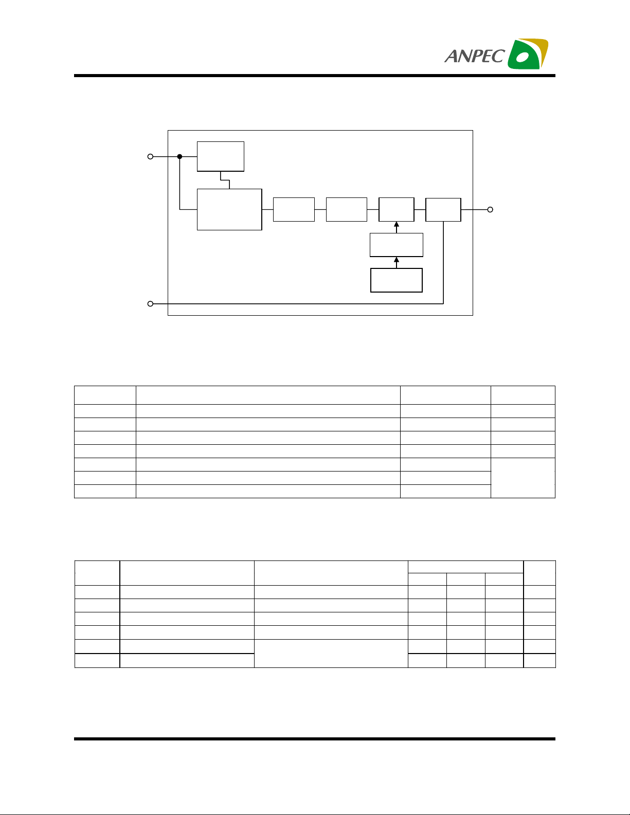
Block Diagram
V
DD
Reverse
Voltage
Protection
APX9031
Temperature
Compensated
Voltage
Regulator
Hall
Element
Current
Amplifier
Latch
Circuit
Hysteresis
Control
Sensitivity
Control
Output
Buffer
Output
Gnd
Absolute Maximum Ratings T
= 25°C unless otherwise noted
A
Symbol Parameter Rating Unit
V
DD
I
DD
I
O
P
D
T
A
T
STG
T
S
Supply Voltage 20 V
Supply Current 8 mA
Output Current 20 mA
Maximum Power Dissipation 400 mW
Operating Ambient Temperature -20 to 85
Storage Temperature Range -55 to 150
Soldering Temperature (10 seconds) 260
C
°
Electical Characteristics
V
V
I
Notes a : use Figure 1
Copyright ANPEC Electronics Corp.
Rev. A.3 - Apr., 2001
Supply Voltage Operating 3 20 V
DD
Output Saturation Voltage I
SAT
I
Supply Current VDD=20V, B<Brp 3.5 6 mA
DD
Output Leakage Current V
Leak
a
t
Output Rise Time 0.6
r
a
t
Output Fall Time
f
OUT
V
TA = 25°C, VDD=12V unless otherwise noted
APX9031Symbol Parameter Test Condition
Min. Typ. Max.
=20mA, B>Bop 0.2 V
=20V, B<Brp 0.5 2
OUT
=12V, RL=820
DD
CL=20pF
Ω,
0.3
www.anpec.com.tw2
Unit
A
µ
s
µ
s
µ

APX9031
Magnetic Characteristics T
Rank
Maximum Operate Point
Bop
= 25°C, VDD=12V unless otherwise noted
A
Maximum Release Point
Brp
Unit
A+70 -70
B +100 -100
Gauss
C +150 -150
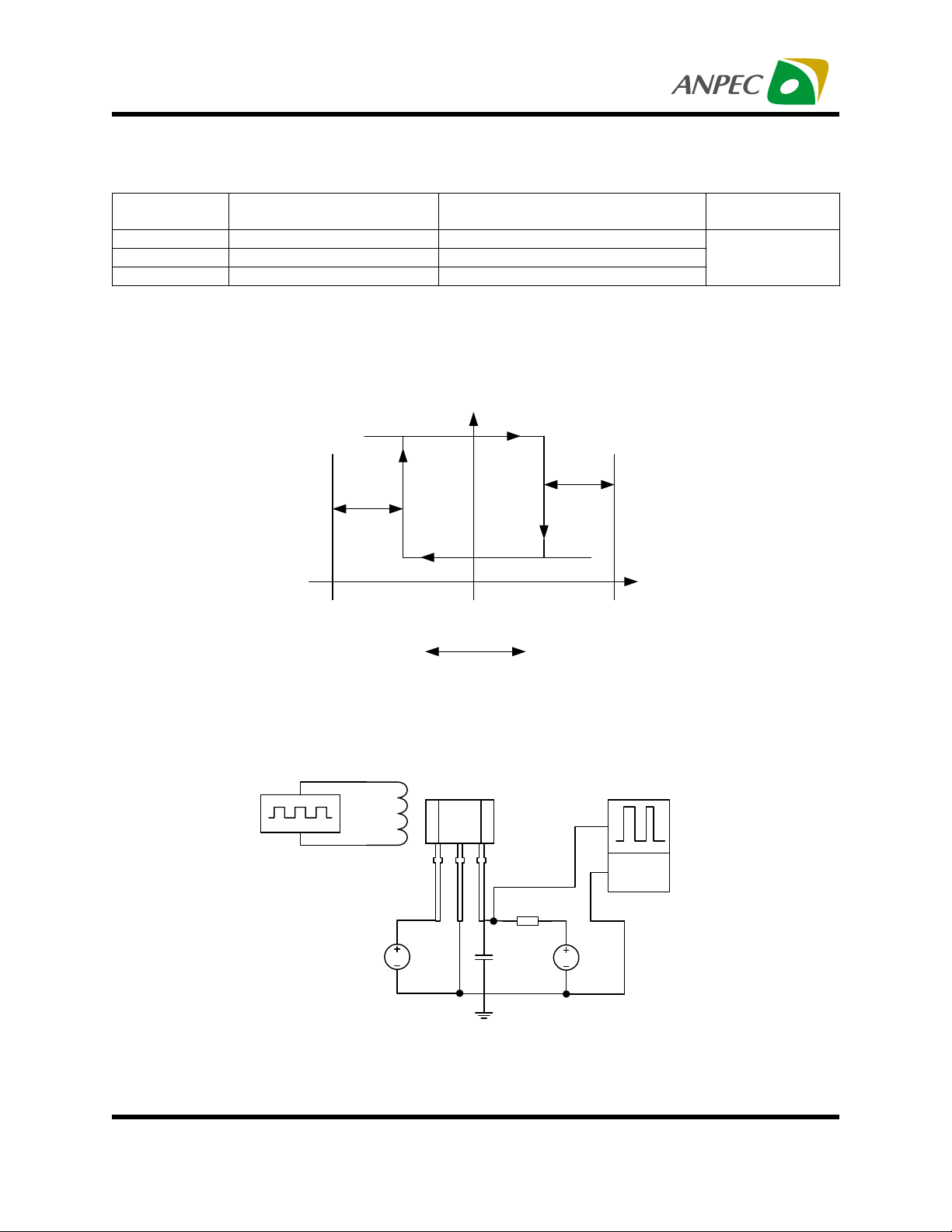
Definition of Magnetic Switching Points and Hysteresis
Output Voltage
Brp min. 0
B
HYS
Bop max.
Test Information
APX9031
23
Signal Generator
Figure 1 : Switching Circuit for Output Rise Time and Fall Time Measurement
1
R
L
V
DD
C
L
Scope
V
DD
Copyright ANPEC Electronics Corp.
Rev. A.3 - Apr., 2001
www.anpec.com.tw3
 Loading...