


APW7066
Dual Synchronous Buck PWM Controll ers and One Linear Controller
Features
• Two Synchronous Buck Converters and
a Linear Regulator
• VIN range up to 12V
• Input Power Supplies Require 12V and 5V or
use 12V to generate a Shunt Regulator 5.8V
• 0.6V Reference for VOUT1 and VOUT3
with 0.8% accurate
• 3.3V Reference for VOUT2 with 0.8% accurate
• Buffered VTT Reference Output
• Three Outputs have Independent Soft-Start
and Enable
• Internal 300kHz Oscillator and Programmable
Frequency range from 70 kHz to 800kHz
• Synchronous Switching Frequency
• DDR mode or Independent Mode Selection
• Phase Shift Selection
• Power Good Function
• Short-Circuit Protection for VOUT1 and VOUT2
• Thermally Enhanced TSSOP-24 and QFN-32
Package
• Lead Free Available (RoHS Compliant)
Applications
• Graphic Cards
• DDR memory Power Supplies
• Low-Voltage Distributed Power Supplies
General Description
The APW7066 has two synchronous buck PWM
controllers and one linear cont roller with high
pre cision internal references voltage to offer accurate
outputs. The PWM controllers are designed to drive
two N-channel MOSFETs in synchronous buck
topology, a nd the linear controller drives an external
N-chan nel MOSFET. The device requires 12V and 5V
power supplies, if the 5V supply is not available,
VCC12 ca n offer an optional shunt regulator 5.8V for
5V supply.
All outputs have independent soft-start and enable
functio ns by SS/EN pins to control. Connect a capacitor
from each SS/EN pin to the ground for setting the
soft-start ti me, and pulling the SS/EN pin below 1V to
disab le regulator. Pull the SS2/EN2 to VCC, enter the
DDR mode, the SS1/EN1 controls both VOUT1 and
VOUT2, and allows VOUT2 to track VOUT1. It also
off ers the phase shift function by REFOUT pin to
sele ct the phase shift between VOUT1 an d VOUT2 in
DDR mode or Independent mode. When all SS/EN
pins exceed 3. 3V and no faults are detected, the
PGOOD pin goes high to indicate the regulators are
ready. If any of t he SS/EN pins goes below 3.2V or
any of the outputs has a fault condition, the PGOOD
pin will be pulled low .
The inte rnal oscillator is nominally 300kHz (keep the
FS/SYN C pin open or short to GND), and it offers the
programmable frequency function from 70kHz t o
800kH z; connecting a resistor from FS/SYNC to VCC
to decrease the frequency, conversely, connect a
resistor fro m FS/SYNC to GND to increase th e frequency.
The IC also provides the synch ronous freque ncy fun ction.
Connect the LGATE signal of another converter to
FS/SYNC pin; forcing the switching frequency to follow
ANPEC reserves the right to make changes to improve reliability or manufacturability without notice, and advise
customers to obtain the latest version of relevant information to verify before placing orders.
Copyright ANPEC Electronics Corp.
Rev. A.4 - Jun., 2005
www.anpec.com.tw1
APW7066
Genera l Description (Cont.)
th e external clock. The possible synchronous frequency
is from 150kHz to 800kHz. There is no Rds(on)
sensing or under-voltage sensing on APW7066.
Howe ver, it provides a simple short-circuit protection
by monitoring the COMP1 a nd COMP2 for over-voltage.
When any of two pins exce eds their trip point and the
condition persists for 1-2 internal clock cycle (3-6us
at 300kHz), the n it will shut down all regulators.
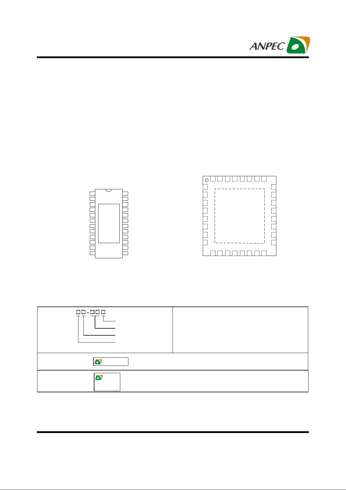
Pin Description
FB1
COMP1
COMP2
FB2
REFIN
REFOUT
SS1/EN1
SS2/EN2
SS3/EN3
VREF
DRIVE3
FB3
1
2
3
4
5
6
7
8
9
10
11
12
GND
BOTTOM
SIDE
PAD
TSSOP-24
TOP VIEW
24
23
22
21
20
19
18
17
16
15
14
13
VCC
BOOT1
UGATE1
VCC12
LGATE1
LGATE2
PGND
UGATE2
BOOT2
GND
PGOOD
FS/SYNC
REFIN
REFOUT
SS1/EN1
SS2/EN2
SS3/EN3
VREF
DRIVE3
Ord ering and Marking Information
APW7066
Lead Free Code
Handling Code
Temp. Range
Package Code
Package Code
R : TSSOP-P * QA : QFN-32
Operating Ambient Temp. Range
C : 0 to 70 C
Handling Code
TU : Tube TR : Tape & Reel
TY : Tray (for QFN only)
Lead Free Code
L : Lead Free Device Blank : Original Device
NC
32
FB2
COMP2
1
8
9
NC
FB3
32 LD 5x5 QFN32
°
FB1
COMP1
GND
BOTTOM
SIDE PAD
PGOOD
FS/SYNC
Top View
VCC
GND
NC
UGATE2
NC
NC
25
BOOT1
16
BOOT2
24
UGATE1
PGND_1
VCC12_1
LGATE1
LGATE2
VCC12_2
PGND_2
NC
17
APW7066 R :
APW7066 QA :
APW7066
XXXXX
APW7066
XXXXX
XXXXX - Date Code
XXXXX - Date Code
Note : ANPEC lead-free products contain molding compounds/die attach materials and 100% matte tin plate
termin ation finish; which are fully compliant with RoHS and compatible with both SnPb and lead-free soldiering
op erations. ANPEC lead-free products meet or exceed the lead-free requirements of IPC/JEDEC J STD-020C
fo r MSL classification at lead-free peak reflow temperature.
Copyright ANPEC Electronics Corp.
Rev. A.4 - Jun., 2005
www.anpec.com.tw2
APW7066
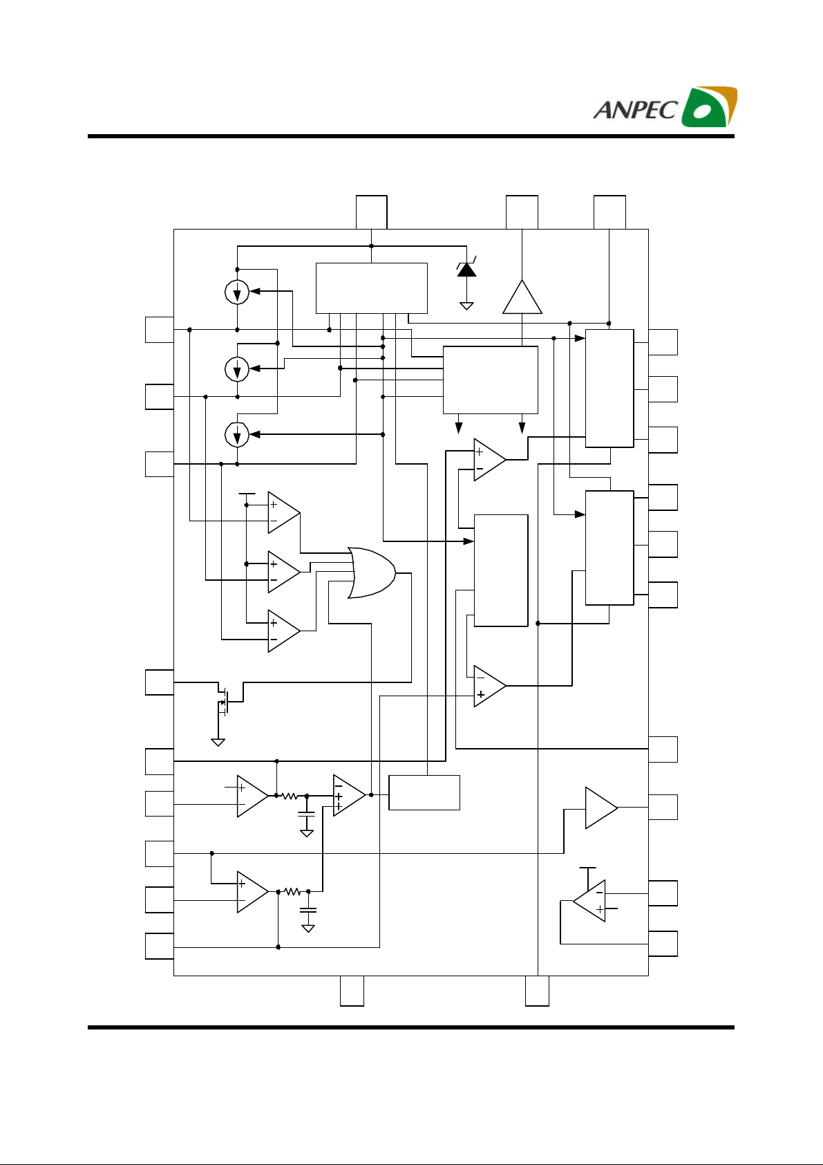
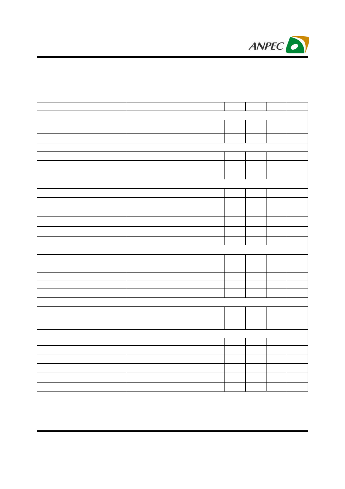
Block Diag ram
SS1/EN1
SS2/EN2
SS3/EN3
3.3V
30uA
30uA
30uA
VCC VREF VCC12
5.8V
Power On Reset and
Control
Bias
Current
0.6V 3.3V
3.3V
Oscillator
Gate
Control
Logic 1
Gate
Control
Logic 2
BOOT1
UGATE1
LGATE1
BOOT2
UGATE2
LGATE2
PGOOD
Monitor COMP Pins
for Short Protection
COMP1
0.6V
FB1
REFIN
FB2
COMP2
Copyright ANPEC Electronics Corp.
Rev. A.4 - Jun., 2005
3.3V
1-2 Clock
Cycle Filter
If short, Filter shut
down all outputs
GND PGND
FS/SYNC
REFOUT
VCC12
FB3
0.6V
DRIVE3
www.anpec.com.tw3
APW7066
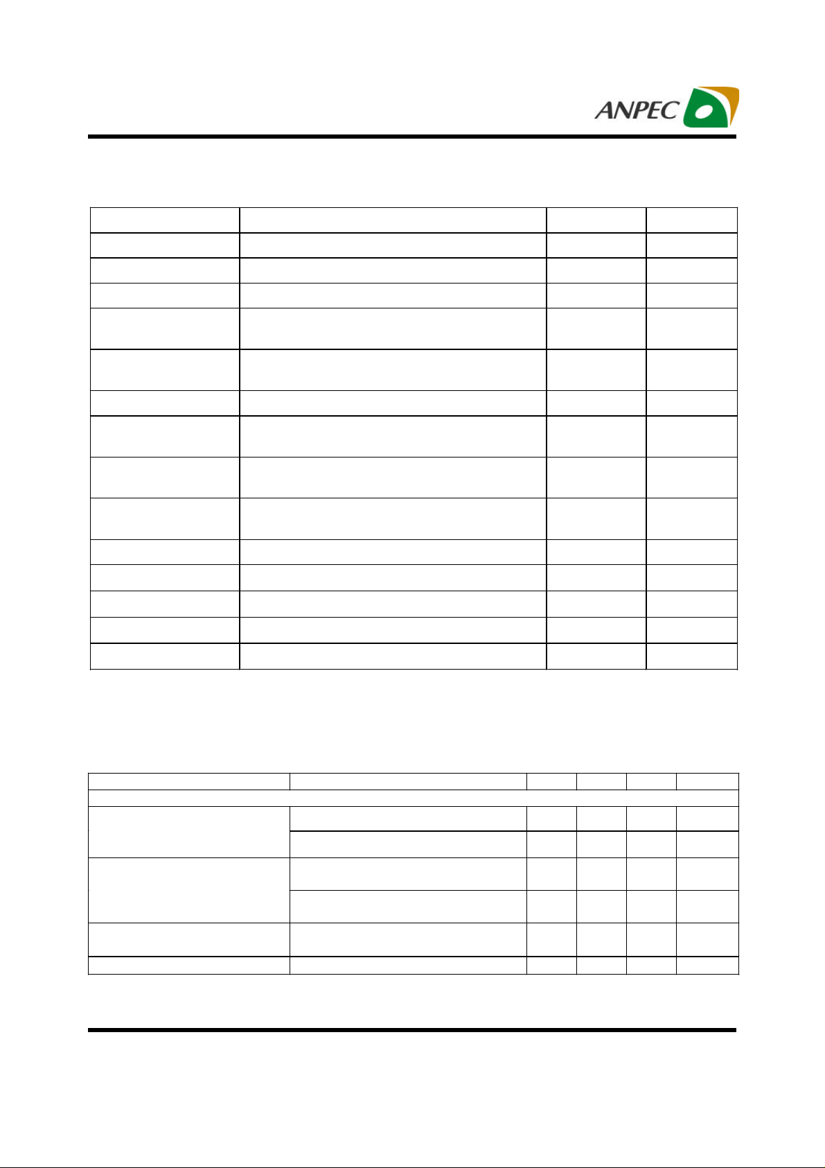
Ab solute Maximum Ratings
Symbol Parameter Rating Unit
VCC12 VCC12 to GND -0.3 to 15 V
VCC, separate supply VCC, separate supply -0.3 to 5.5 V
VCC, shunt regulator VCC, shunt regulator to GND -0.3 to 6 V
UGATE1, UGATE2,
BOOT1, BOOT2
LGATE1, LGATE2,
DRIVE3
FS/SYNC FS/SYNC to GND -0.3 to 15 V
REFIN, REFOUT,
PGOOD, VREF
FB1, COMP1, FB2,
COMP2, FB3
SS1/EN1, SS2/EN2,
SS3/EN3
PGND PGND to GND -0.3 to +0.3 V
TA Operating Temperature Range 0 to +70
TJ Maximum Junction Temperature +150
T
Storage Temperature Range -65 to +150
STG
TL Lead Temperature (Soldering, 10sec) 260
UGATE1, UGATE2, BOOT1, BOOT2 to GND -0.3 to 30 V
LGATE1, LGATE2, DRIVE3 to GND -0.3 to 15 V
REFIN, REFOUT, PGOOD, VREF to GND -0.3 to VCC V
FB1, COMP1, FB2, COMP2, FB3 to GND -0.3 to VCC V
SS1/EN, SS2/EN2, SS3/EN3 to GND -0.3 to VCC V
Ele ctrical Characteristics
°
C
°C
°C
°C
Operating Conditions: VCC = 5V, VCC12 = 12V, TA = 0 to 70°C, Unless Otherwise Specified.
Parameter Test Conditions Min. Typ. Max. Units
INPUT SUPPLY POWER
Input Supply Current
(Quiescent)
Input Supply Current (Dynamic)
Shunt Regulator Output Voltage
Shunt Regulator Current
VCC; outputs disabled
VCC12; outputs disabled
VCC12; UGATEs, LGATEs CL = 1nF,
300KHz
VCC; UGATEs, LGATEs CL = 1nF,
300KHz
20mA current; ~Equivalent to 300Ω
resistor VCC to 12V
300Ω resistor VCC to 12V
4 mA
6 mA
50 mA
7 mA
5.6 5.8 6.0 V
20 60 mA
Copyright ANPEC Electronics Corp.
Rev. A.4 - Jun., 2005
www.anpec.com.tw4
APW7066
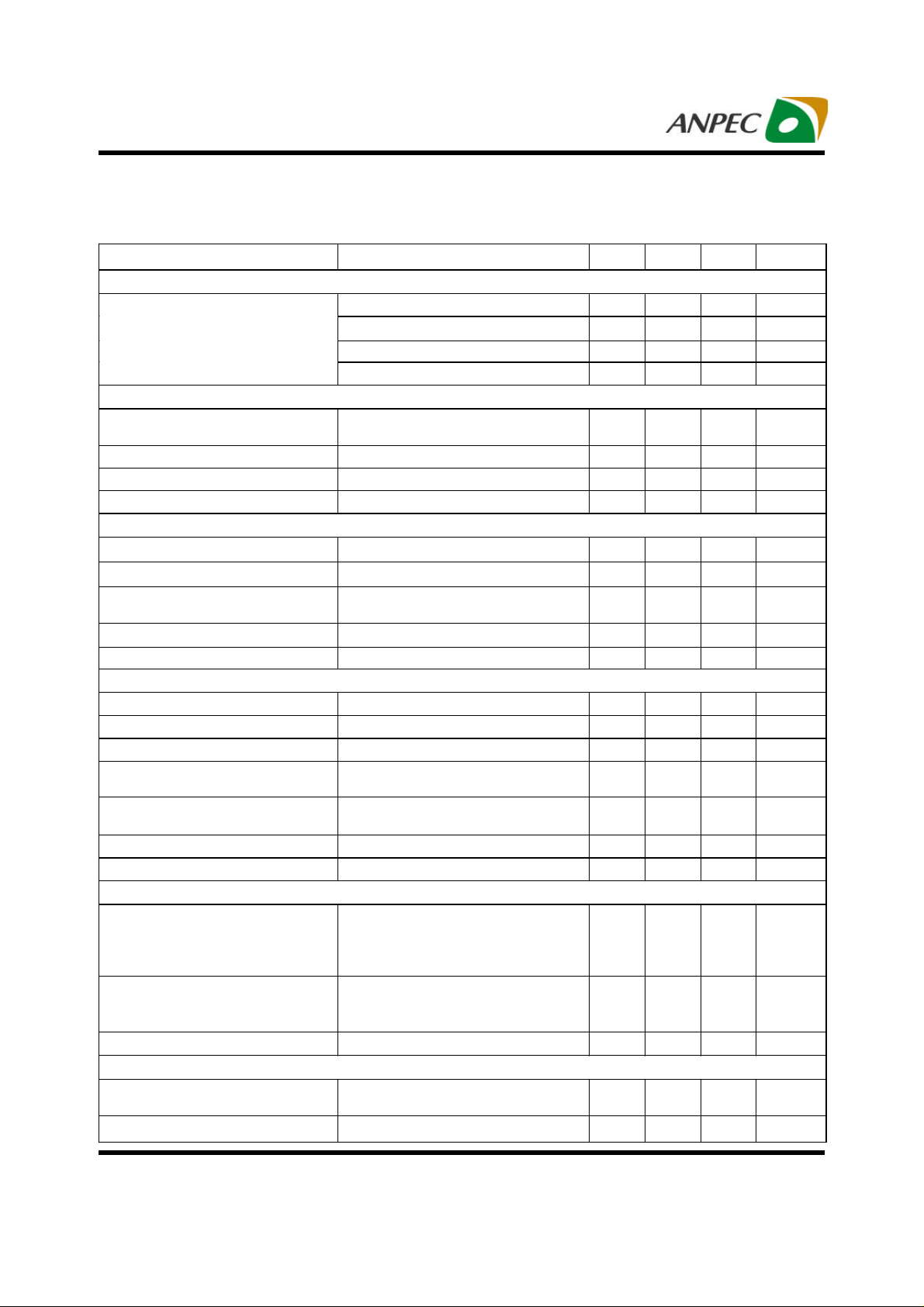
ND;
DRIVE3 to FB3; compare to internal
Ele ctrical Characteristics (Cont.)
Operating Conditions: VCC = 5V, VCC12 = 12V, TA = 0 to 70°C, Unless Otherwise Specified.
Parameter Test Conditions Min. Typ. Max. Units
INPUT SUPPLY POWER
VCC Rising 4.15 4.23 4.4 V
Power-On Reset Threshold
SYSTEM ACCURACY
Outputs 1 and 3 Reference
Voltage
Output 2 Reference Voltage 3.3V
Outputs 1 and 2 System Accuracy -0.8 0.8 %
Output 3 System Accuracy -0.8 0.8 %
OSCILLATOR
Accuracy -20 20 %
Frequency FS/SYNC pin open 240 300 360 KHz
Adjustment Range
Sawtooth Amplitude 2.1 V
Duty-Cycle Range 0 85 %
ERROR AMPLIFIER (OUT1 and OUT2)
Open-Loop Gain
Open-Loop Bandwidth
Slew Rate
EA Offset COMP1/2 to FB1/2; compare to
Maximum Output Voltage
Output High Source Current COMP1/2, VCOMP=2V
Output Low Sink Current COMP1/2, VCOMP=2V
PROTECTION AND MONITOR
Under-Voltage Threshold
(COMP1 and COMP2)
UV filter time
PGOOD Low Voltage IPGOOD = 2mA 0.1 0.3 V
LINEAR REGULATOR (OUT3)
VCC Falling 3.9 4.0 4.15
VCC12 Rising 7.55 7.8 8 V
VCC12 Falling 7.1 7.3 7.55
FS/SYNC pin: resistor to G
resistor to VCC12
RL = 10kΩ to ground
CL = 100pF, RL = 10kΩ to ground
CL = 100pF, RL = 10kΩ to ground
internal VREF/REFIN
RL = 10kΩ to ground; (may trip
short-circuit)
Causes PGOOD to go low; if there
for a filter time, implies the COMP
pin(s) is out-of-range, and shuts
down IC
Based on internal oscillator clock
frequency (nominal 300kHz = 3.3µs
clock period)
0.6 V
70 800 KHz
85 dB
15 MHz
4
2
VCC
-50 mA
45 mA
3.3
1 2
V
V
V/µs
mV
V
V
Clock
pulses
EA Offset
DRIVE3 High Output Voltage
Copyright ANPEC Electronics Corp.
Rev. A.4 - Jun., 2005
VREF
2 mV
VCC12
www.anpec.com.tw5
APW7066
Ele ctrical Characteristics (Cont.)
Operating Conditions: VCC = 5V, VCC12 = 12V, TA = 0 to 70°C, Unless Otherwise Specified.
Parameter Test Conditions Min. Typ. Max. Units
LINEAR REGULATOR (OUT3)
DRIVE3 High Output Source
Current
DRIVE3 Low Output Sink Current
VREF
Output Voltage
Output Accuracy
Source Current
REFOUT (VTTREF)
Output Voltage Determined by REFIN voltage
Offset Voltage
Source Current
Sink Current
Output Capacitance
Output High Voltage Minimum To select 0 degree phase; see Table 1
ENABLE/SOFTSTART (SS/EN 1,2,3)
Enable Threshold
Soft-Start Current
Soft-Start High Voltage End of ramp
Output High Voltage To select DDR mod; see Table 1
FS/SYNC PLL
Frequency range of Lock-in
High Voltage
GATE DRIVERS
Output1 GATE Driver Source UGATE1, LGATE1=3V, BOOT=12V 1.8 A
Output2 GATE Driver Source UGATE2, LGATE2=3V, BOOT=12V 1 A
Output1 GATE Driver Sink UGATE1, LGATE1=3V, BOOT=12V 2.5
Output2 GATE Driver Sink UGATE2, UGATE2=3V, BOOT=12V 4
Output Voltage UGATE1, UGATE2 30 V
Output Voltage LGATE1, LGATE2 12 V
1.1µF max capacitance
EN Rising
EN falling
( from LG pin of another IC, for
example)
1.5 mA
2.5 mA
3.3 V
-0.8 +0.8
2.0 mA
0.6 3.3 V
-10 +10 mV
0.2 20 mA
0.48 mA
0.1 µ
3.8 VCC
1.05
0.95
-30
3.5 V
3.8 VCC
150 800 KHz
12 V
V
µ
%
F
V
A
V
Ω
Ω
Copyright ANPEC Electronics Corp.
Rev. A.4 - Jun., 2005
www.anpec.com.tw6
APW7066
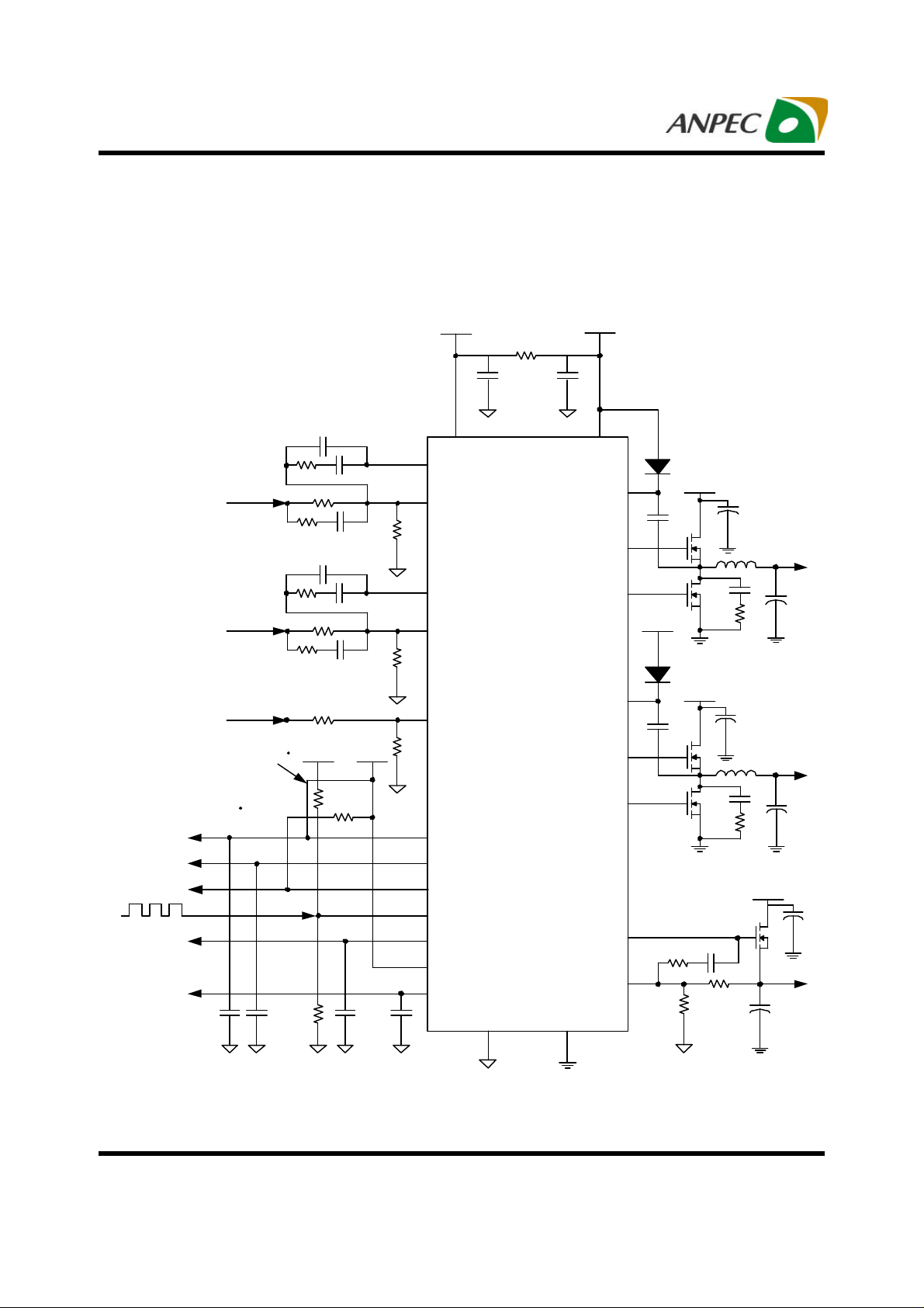
Typical Application Circuit
APW706 6
DDR MODE
VOUT1
VOUT2
VOUT1(DDR)
PHASE
SHIFT 0
VCC12
VCC
VCC
COMP1
FB1
COMP2
FB2
REFIN
Optional for
shunt regulator
APW7066
VCC12
BOOT1
UGATE1
LGATE1
BOOT2
UGATE2
VIN1
VOUT1
VCC12
VIN2=VOUT1(DDR)
VOUT2
PHASE
SHIFT 90
VTTREF
Copyright ANPEC Electronics Corp.
Rev. A.4 - Jun., 2005
REFOUT
VREF
PGOOD
FS/SYNC
SS1/EN1
SS2/EN2
SS3/EN3
GND PGND
LGATE2
DRIVE3
FB3
VIN3
VOUT3
www.anpec.com.tw7
APW7066
Typ ical Application Circuit (Cont.)
APW706 6
IND EPENDENT MODE
PHASE
SHIFT 180
VTTREF
SYNCHRONOUS
FREQUENCY
VOUT1
VOUT2
VREF
PHASE
SHIFT 0
VCC12
VCC
VCC
COMP1
FB1
COMP2
FB2
REFIN
REFOUT
VREF
PGOOD
FS/SYNC
SS1/EN1
Optional for
shunt regulator
APW7066
VCC12
BOOT1
UGATE1
LGATE1
BOOT2
UGATE2
LGATE2
DRIVE3
VIN1
VOUT1
VCC12
VIN2
VOUT2
VIN3
Copyright ANPEC Electronics Corp.
Rev. A.4 - Jun., 2005
SS2/EN2
SS3/EN3
GND PGND
FB3
VOUT3
www.anpec.com.tw8

APW7066
Function Pin De scriptions
VCC
Powe r supply input pin. Connect a nominal 5V power
supply to this pin for the control circuit, or connect a
resistor (nominally 300Ω) to VCC12 for a shunt
regulator function (typical 5.8V). It is recommended
that a de coupling capacitor (1 to 10uF) is connected
to the GND for noise decoupling.
GND
This pin is the signal ground pin. The metal thermal
pad und er the package is the IC substrate; connects
the GND pin and metal thermal pad together on the
board, and ties to the good GND p lane for electrical
and thermal con duction.
VC C12
Pow er supply input pin. Connect a no minal 12V power
su pply to this p in for the ga te driver. It is re commended
that a decoupling ca pacitor (1 to 10uF) is connected
to the GND for n oise decoupling.
PGND
This pin is the power grou nd pin for the gate driver a nd
linear driver circuit. It should be tied to the GND.
FB1, FB 2, FB3
These pins are th e inverting inputs of the error amplifiers of their respective regulators. They are used to
set the output voltage and the compensation
components.
SS1/EN1, SS2/EN2, SS3/EN3
These pins provide two functions. Connect a capacitor
to the GND fo r setting the soft-start time. Use an open
drain log ic signal to pull the SS/EN pin low to disable
the respective output, leave open to enable the respe ctive output.
COMP1 , COMP2
These pin s are the outputs of error amplifiers of their
respect ive regulators. They are used to set the
compensa tion components.
UGATE1, UGATE2
These pins provide t he gate driver for the upper
MOSFETs of VOUT1 a nd VOUT2.
LGATE1, LGATE2
These pins provide the gate driver for the lower
MOSFETs of VOUT1 and VOUT2.
BOOT1, BOOT2
These pins provide the bootstrap voltage to the gate
driver for driving the upper MOSFETs. It can be
connected to a power voltage directly, but the difference voltage between the BOOT a nd VIN must be high
enoug h to drive the upper MOSFETs.
REFIN
This pin is th e refere nce input voltag e of error amplifier
of the VOUT2. It also provides the volta ge into a buffe r,
which is ou t on the REFOUT pin.
REFOUT
This pin provides a buffed voltage, which is from REFIN
pin. In Independent mode, it can be used by other
ICs. In DDR mode, it is from th e VOUT1, and can be
use d as the VTT buffer.
This p in also uses to select th e phase shift (see table1 ).
When this pin pulls to VCC, the buffer is disabled and
the REFOUT is not available for use. It is reco mmended
that a 0.1u F capacitor is connected to the ground for
stability.
VR EF
This p in provides a 3.3V refe rence voltage, which can
be used by the REFIN pin or other ICs as a voltage
reference. It is recommended that a 1uF capacitor is
connected to ground for stability.
DRIVE3
This pin drives the gate of an external N-channel
MOSFET for line ar regulator.
PGOOD
This pin is an open drain device; connect a pull up
resistor to the VCC for PGOOD function.
FS/SYN C
This pin is used to adjust the switching frequency.
Con necting a resistor fro m FS/SYNC pin to the ground
increases the switching frequency. Conversely, connecting a resistor from this pin to the VCC12 reduces
the swit ching frequency. In addition, this pin also
provide s synchronous frequency function. An e xternal
clock can be fed into this pin, and force the switching
frequency to follow the external clock.
Copyright ANPEC Electronics Corp.
Rev. A.4 - Jun., 2005
www.anpec.com.tw9
APW7066
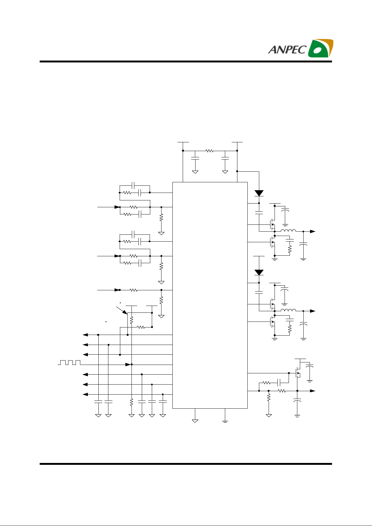
Typ ical Characteristics
VOUT1 Po wer Up
VCC12(5V/div)
VCC(2V/div)
VOUT1(1V/div)
SS1(2V/div)
Time(5ms/div)
VOUT2 Po wer Up
VCC12(5V/div)
VCC(2V/div)
VOUT2(2V/div)
SS2(2V/div)
Time(5ms/div)
VOUT3 Po wer Up VREF Power Up
VCC12(5V/div)
VCC(2V/div)
VOUT3(1V/div)
SS3(2V/div)
Time(5ms/div)
Copyright ANPEC Electronics Corp.
Rev. A.4 - Jun., 2005
VCC12(5V/div)
VCC(2V/div)
VREF(2V/div)
SS2(2V/div)
Time(5ms/div)
www.anpec.com.tw10
APW7066
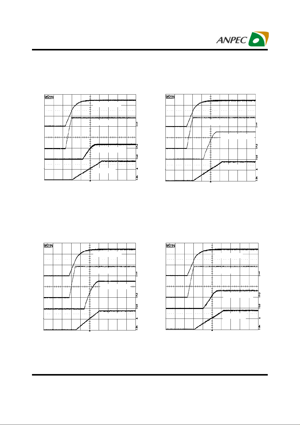
Typ ical Characteristics (Cont.)
VOUT1 Po wer Up
VOUT1(1V/div)
SS1(2V/div)
UGATE1(20V/div)
LGATE1(10V/div)
Time(2ms/div)
VOUT2 Po wer Up
UGATE2(20V/div)
LGATE2(10V/div)
VOUT2(5V/div)
SS2(2V/div)
Time(2ms/div)
DDR Mod e Power Up
VREF(2V/div)
VOUT2(2V/div)
VOUT1(1V/div)
SS1(2V/div)
Time(2ms/div)
Copyright ANPEC Electronics Corp.
Rev. A.4 - Jun., 2005
SS2=VCC
VOUT1= REFIN
Phase Shift 0 degrees
LG1(10V/div)
LG2(10V/div)
Time(1u s/div)
www.anpec.com.tw11
APW7066
Typ ical Characteristics (Cont.)
Phase Shift 90 degrees
LG1(10V/div)
LG2(10V/div)
Time(1u s/div)
Phase Shift 180 degrees
LG1(10V/div)
LG2(10V/div)
Time(1u s/div)
PGOOD High PGOOD Low
SS1(2V/div)
SS2(2V/div)
SS3(2V/div)
PGOOD(5V/div)
Time(5ms/div)
Copyright ANPEC Electronics Corp.
Rev. A.4 - Jun., 2005
SS1(2V/div)
SS2(2V/div)
SS3(2V/div)
PGOOD(5V/div)
Time(5ms/div)
www.anpec.com.tw12
APW7066
Typ ical Characteristics (Cont.)
VOUT2 Sho rt Circuit Protection
Comp2 (2V/div)
SS2 (2V/div)
UG2 (20V/div)
PGOOD (5V/div)
Time(5u s/div)
VOUT1 Sho rt Circuit Protection
Comp1 (2V/div)
SS1 (2V/div)
UG1 (20V/div)
PGOOD (5V/div)
Time(5u s/div)
VOUT1 Load Transient
VOUT1 (0.2V/div)
VOUT2 (0.1V/div)
VOUT3 (0.1V/div)
IOUT1 (10A/div)
Time(20 us/div)
Copyright ANPEC Electronics Corp.
Rev. A.4 - Jun., 2005
VOUT1=VIN3
VOUT2 Load Tran sient
VOUT1 (0.1V/div)
VOUT2 (0.1V/div)
VOUT3 (0.05V/div)
IOUT2 (5A/div)
VOUT1=VIN3
Time(20 us/div)
www.anpec.com.tw13

APW7066
Typ ical Characteristics (Cont.)
VOUT3 Load Transient UG1 Rising
VOUT1=VIN3
VOUT1 (0.1V/div)
VOUT2 (0.1V/div)
UG1 (10V/div)
Phase1 (10V/div)
VOUT3 (0.1V/div)
IOUT3 (2A/div)
Time(20 us/div)
UG1 Falling
UG1 (10V/div)
Phase1 (10V/div)
LG1 (10V/div)
Time(50 ns/div)
UG2 R ising
UG2 (10V/div)
Phase2 (10V/
LG1 (10V/div)
Time(50 ns/div)
Copyright ANPEC Electronics Corp.
Rev. A.4 - Jun., 2005
LG2 (10V/div)
Time(50 ns/div)
www.anpec.com.tw14

APW7066
Typ ical Characteristics (Cont.)
UG2 Falling
LG2 (10V/div)
Time(50 ns/div)
UG2 (10V/div)
Phas e2 (10V/div)
PGOOD Sink Curre nt vs. PGOOD Voltage
3
2.5
2
1.5
1
Sink Current (mA)
0.5
0
0 10 20 30 40
PGOOD Voltage (mV)
REFOUT Vo ltage vs. Source Current
3.35
3.34
3.33
3.32
3.31
3.3
3.29
3.28
3.27
REFOUT Voltage (V)
3.26
3.25
0 5 10 15 20
Source Current (mA)
Copyright ANPEC Electronics Corp.
Rev. A.4 - Jun., 2005
VREF Voltage vs. Source Current
3.32
3.31
3.3
3.29
VREF Voltage (V)
3.28
0 0.5 1 1.5 2
Source Current (mA)
www.anpec.com.tw15

APW7066
Typ ical Characteristics (Cont.)
UG1 Sink Current vs. Volta ge
2.4
2.2
2
1.8
1.6
1.4
1.2
1
0.8
Sink Current (A)
0.6
0.4
0.2
0
0 2 4 6 8 10 12
UG1 Volta ge (V)
UG1 Sou rce Current vs. Voltage
2.4
2.2
2
1.8
1.6
1.4
1.2
1
0.8
0.6
Source Current (A)
0.4
0.2
0
0 2 4 6 8 10 12
UG1 Volta ge (V)
LG1 Sink Current vs. Voltage
2.4
2.2
2
1.8
1.6
1.4
1.2
1
0.8
0.6
Sink Current (A)
0.4
0.2
0
0 2 4 6 8 10 12
LG1 Voltage (V)
Copyright ANPEC Electronics Corp.
Rev. A.4 - Jun., 2005
LG1 Sou rce Current vs. Voltage
2.4
2.2
2
1.8
1.6
1.4
1.2
1
0.8
0.6
Source Current (A)
0.4
0.2
0
0 2 4 6 8 10 12
LG1 Voltage (V)
www.anpec.com.tw16

APW7066
Typ ical Characteristics (Cont.)
UG2 Sink Current vs. Volta ge
1.6
1.4
1.2
1
0.8
0.6
0.4
Sink Current (A)
0.2
0
0 2 4 6 8 10 12
BOOT=12V
UG2 Volta ge (V)
UG2 Sou rce Current vs. Voltage
1.4
BOOT=12V
1.2
1
0.8
0.6
0.4
Source Current (A)
0.2
0
0 2 4 6 8 10 12
UG2 Voltage
LG2 Sink Current vs. Voltage
1.6
1.4
1.2
1
0.8
0.6
0.4
Sink Current (A)
0.2
0
0 2 4 6 8 10 12
LG2 Voltage (V)
Copyright ANPEC Electronics Corp.
Rev. A.4 - Jun., 2005
LG2 Sou rce Current vs. Voltage
1.4
1.2
1
0.8
0.6
0.4
Source Current (A)
0.2
0
0 2 4 6 8 10 12
LG2 Voltage (V)
www.anpec.com.tw17

APW7066
Typ ical Characteristics (Cont.)
DRIVE3 Sink Curre nt vs. Voltage DRIVE3 Source Current vs. Voltage
3.5
3
2
2.5
2
1.5
1
Sink Current (mA)
0.5
0
0 2 4 6 8 10 12
DRIVE3 Volta ge (V) DRIVE3 Volta ge (V)
FS Resistance vs. Switching Frequen cy
1000
FS to VCC12
900
800
700
600
500
400
300
200
FS Resistance (kΩ)
100
0
0 100 200 300 400 500 600 700 800
FS to GND
Switching Freq uency (kHz)
1.5
1
0.5
Source Current (mA)
0
0 2 4 6 8 10 12
Shunt Re gulator Sink Current vs. Voltage
60
50
40
30
20
Sink Current (mA)
10
0
3 3.5 4 4.5 5 5.5 6 6.5 7
Shunt Re gulator Voltage (V)
Copyright ANPEC Electronics Corp.
Rev. A.4 - Jun., 2005
www.anpec.com.tw18

APW7066
Typ ical Characteristics (Cont.)
Comp Sink Current vs. Volta ge
60
50
40
30
20
Sink Current (mA)
10
0
0 0.5 1 1.5 2 2.5 3
Comp Volta ge (V)
Comp Sou rce Current vs. Voltage
70
60
50
40
30
20
Source Current (mA)
10
0
0 1 2 3 4
Comp Volta ge (V)
FB Voltag e vs. Temperature
610
608
606
604
602
600
598
596
FB Voltage (V)
594
592
590
0 25 50 75 100 125 150
Temperature (°C)
Copyright ANPEC Electronics Corp.
Rev. A.4 - Jun., 2005
VREF Voltage vs. Temperature
3.35
3.34
3.33
3.32
3.31
3.3
3.29
3.28
VREF Voltage (V)
3.27
3.26
3.25
0 25 50 75 100 125 150
Temperature (°C)
www.anpec.com.tw19

APW7066
REFOUT
Function Descriptions
Operational Modes
The APW706 6 has two inde pendent synchronous buck
converters, and it also has DDR mode operation to
allow VOU T2 to track VOUT1.
In indepe ndent mode operation, connect a capacitor
from each SS/EN pin t o the ground to set each
regulator’s soft-start time. The 3.3V reference VREF
can be used directly, or divided by two resistors for
REFIN, since the VREF is controlled by the SS2/EN2.
DDR mode is chosen by conne cting the SS2/EN2 pin
to VCC(5V). In this mode, SS2/EN2 function w ill be
disabled, SS1/EN1 is used to control soft start and
enab le both VOUT1 and VOUT2. The VOUT1 is used
as the REFIN for the VOUT2, that makes VOUT2 to
track VOUT1.
VREF
REFIN
SS1/EN1
SS2/EN2
SS3/EN3
GND
Phase Shift
The APW7066 has phase shift function, use the
REFOUT pin to select the phase shift between
Independent mode and DDR mode. Connect the
REFOU T to VCC to get the 0 degrees in either mode.
In this case, the buffer of the REFOUT is disabled.
Lea ve the REFOUT open shifts the phase 90 degrees
in DDR mode, or 180 degree s in Independent mode,
REFOUT ca n be used in this case ( see Table 1.).
MODE SS2/EN2
DDR VCC VCC VOUT1 0 deg
DDR VCC Open VOUT1 90 deg
Independent SS2 cap VCC VREF
Independent SS2 cap Open VREF 180 deg
Table1.Mo de and Phase Se lection
REFIN PHASE SHIFT CH1/CH2
SS1/EN1 for CH1
and CH2
0 deg
SS1/EN1 for CH1
SS2/EN2 for CH2
The advanta ge of Phase shift is to avoid overlapping
the switching current spikes of the two channels, or
interaction betw een the channels; it also reduces the
RMS current of the input capacitors, allowing f ewer
caps to be employed. However, the phase shift
betwee n the rising edge of LGATE1 and L GATE2 (See
figure 3.), depending on the duty cycles, the falling
edges of the two channels might overlap; so the user
should check it.
Figure 1. Indep endent Mode Circuit
VOUT1
VCC
SS1/EN1
SS2/EN2
SS3/EN3
Figure 2.DDR Mode Circuit
Copyright ANPEC Electronics Corp.
Rev. A.4 - Jun., 2005
REFIN
GND
LG1
LG2
(0deg)
LG2
(90deg)
LG2
(180deg)
0 90 180 0
Figure 3 . Phase of LG2 with respect
to rising edge of LG1
www.anpec.com.tw20

APW7066
I
Function De scriptions (Cont.)
Soft-Start/Enable
The three SS/EN pins control the soft-start and enable
or disable the controller. In Independent mode, the
three regulators all have independent soft-start and
enable functions. Co nnect a soft-start capacitor from
each SS/EN pin to the GND to set the soft-start
interval, and an open dra in logic signal for each SS/EN
pin w ill enable or disable the respective output.
Figu re 4. Show s the soft-start interval. Whe n both VCC
and VCC12 reach their Power-On-Reset threshold
4.23V and 7.8V, a 30uA current source starts to
charge the capacitor. When t he SS reaches the
enabled t hreshold about 1V, the internal 0.6V
reference starts to rise and follows the SS; the error
amplifier output (COMP) suddenly raises to 1.1V, which
is the valley of the oscillator’s triangle wave, leads the
VOUT to start up. Until the SS reaches about 3.0V,
the internal reference completes the soft-start interval
a nd reaches to 0.6V; then VOUT1 is in regu lation. The
SS1 still rises to 3.5V and then stops.
VOLTAGE
VSS
3V
VOUT
1V
t1 t2t0
Figure 4. Soft-Start Inte rval
C
SS
ttT
12Start-Soft ⋅=−=
2V
SS
Where :
CSS = external Soft-Start ca pacitor
ISS = Soft-Start current = 30µA
TIME
PGOOD
The PGOOD output is an open-drain device, when the
VCC is prese nt; the gate of open-drain device will be
high, forcing the PGOOD pin to go low. T he three
SS/EN pins and the SCP signals control the PGOOD
signal (see block diagram), after the t hree SS/EN
signals a re over threshold high 3.3V and three outputs
have no short -circuit, the PGOOD goes high to
indicate all regulators are re ady. If any of the SS/EN
pins goes below th reshold low 3.2V, the PGOOD will
go low. Also, if any of the outputs has a short, the
PGO OD pull low and if short-circuit condition
continues for 1-2 clock pulse s, all regulators will shut
down. If the short-circuit is not long enough to shut
down , it may still cause PGOOD to g o low momentarily.
Because the PGOOD is an open-drain device, the
typical range of the value to connect a pull high
resistor to VCC will be 1kΩ to 10kΩ; if PGOOD is not
used, leave it open.
Shunt Regulator
The APW7066 must have two power supplies VCC
(5V) a nd VCC12 (12V) to drive the IC; VCC (5V) is for
the control circu it and VCC12 (12V) is for the drivers
of output s. But it can also operate only VCC12,
because the shunt regulator 5.8V was designed for
VCC (5V); the range of the shunt regulator was design ed over the usual range 4.5V to 5.5V of typical 5V
power supplies.
Connect a resistor from VCC12 to VCC for shunt
regulator and for the su pply current. The input supply
current of VCC is 7mA; minimum shunt regulator
current is about 7mA, a nd therefore the 20mA shunt
regulator current is enough; thus, the typical value,
300Ω of the resistor is recommended. The relation
amon g minimun shunt regula tor current, requ ired shu nt
regulator current and supp ly current is:
Copyright ANPEC Electronics Corp.
Rev. A.4 - Jun., 2005
www.anpec.com.tw21

APW7066
Switching Frequency (kHz)
FS Resistance (kO)
Function De scriptions (Cont.)
PGOOD (Cont.)
ISHUNT = ICC + ISHUNT(MIN)
Where :
ISHUNT = Re quired Shunt Regulator Current
ICC = Supp ly Current
ISHUNT(MIN) = Minimum Shu nt Regulator Current
VCC (5.8V)
OPTIONAL R
FOR SHUNT
REGULATOR
VCC12
Oscillator
The APW7066 provides the oscillator swit ching
f requency adjustment. Connect a resistor from
FS/SYNC pin to the ground, the nominally 300kHz
oscillator switching frequency is increased according
to the value of the re sistor. The adjustment range of
the switching freque ncy is 300kHz to 800kHz.
Converse ly, connecting a resistor from FS/SYNC pin
to the VCC12 reduces the switching frequency.The
adjustment ra nge of the switching frequency is 70kHz
to 30 0kHz.
1000
FS to VCC12
900
800
700
600
500
400
300
200
100
0
0 100 200 300 400 500 600 700 800
FS to GND
SYN C
The switching frequen cy also can be synchronized to
an external frequency. If there are two switching
converters on t he same board, taking the LGATE
sign al from another switching converter, go through a
10kΩ resistor, and conne cting to the FS/SYNC pin.
The APW7066 will read another converter’s freq uency
and after several milliseconds, the APW7066 will
change to new frequency. If ano ther converter’s signal
is lost, the APW7066 will return to internal oscillator.
This a llows the two switching converters for operating
at th e same frequency to avoid the interference from
the independent frequencies between them. The
a cceptable frequency is a range of 150kHz to 800kHz.
Short-Circuit Protection
The APW7066 has a simple short-circuit protection
to monitor COMP1 and COMP2 for VOUT1/2. When
output voltage has a short, the FB p in should start to
follow output, since it is a resistor divider from the
output. The FB is the inverting input of Error-Amp,
when FB pin is lower than the Error-Amp reference,
then the COMP will rise to increase the duty-cycle of
the up per MOSFET gate driver, this allows output to
get high er voltage. If the short-circuit condition is long
enou gh, the COMP pin will exceed the trip point 3.3V,
and the duty circle w ill hit the maximum. This means
that either Over-Cu rrent or Under-Voltage condition is
detected. If an y of the COMP1 and COMP2 exceeds
their trip po ints, and holds over a filter time (1-2 clock
cycle of switching frequency), then all regu lators will
shut down, and require a POR on either of VCC or
VCC12 to restart. Note that the linear regulator has
no short-circuit prote ction.
Figure 5. FS/SYNC Resistance vs. Frequen cy
Copyright ANPEC Electronics Corp.
Rev. A.4 - Jun., 2005
www.anpec.com.tw22

APW7066
Applica tion Information
Output Voltage Setting
The output voltage can be adjusted with a resistive
divider, from ou tput voltage to FB pin to the ground.
Use 1% or better resistors for these resistor dividers
is recommended. The reference voltages of VOUT1
and VOUT3 are 0.6V, the reference voltage of VOUT2
is REFIN voltage. The VREF voltage is for REFIN in
independent mode. The following equations can be
used to calculate the outpu t voltage:
R1
R2
R1
R2
R1
R2
R3
0.6V x )
REFIN x )
0.6V x )
Mode) (DDR x VOUT1)
1(VOUT1 +=
1VOUT2 +=(
1VOUT3 += (
(1REFIN +=
R4
R3
(1REFIN +=
R4
Where :
R1 = re sistor from VOUT to FB
R2 = resistor from FB to GND
R3 = resistor from VREF or VOUT1 to REFIN
R4 = resistor from REFIN to GND
Note that the R1 is part of the compensation . It should
be conformed to the feedback compensation.
Line ar Regulator Input/Output MOSFET Selection
The maximum DR IVE3 voltage is determined by the
VCC12. Since this pin drives an external N-channel
MOSFET, therefore the maximum output voltage of
the linear regulator is depend ent upon the VGS.
VOUT3MAX = VCC12 - VG S
Another criteria is its efficiency of heat removal. The
power dissipated by the MOSFET is given by:
Pdiss = Iout x (VIN - VOUT3)
whe re Iout is the maximum load current VOUT3 is the
nominal output voltage
In some applications, heatsink might be required to
help mainta in the junctio n temperature of the MOSFET
below its maximum rating.
Linear Regulator Compensation Sele ction
The linear regulator is stable over all load current.
Mode) nt(Independe x VREF)
However, the transient response can be further
enhanced by connecting a RC network between the
FB3 and DRI VE3 pin. Depending on the output
capacitance and load current of the application, the
value of this RC network is then varied. A good starting
point for the resistor value is 6.8kΩ and 470pF for the
ca pacitor.
PWM Compensation
Linear Regulator Input/Output Capacitor Selection
The input capacitor is chosen based on its voltage
rating. Under load transient condition, the input
capacit or will momentarily supply the required
tran sient current. The output capacitor for the linear
regula tor is chosen to minimize any droop during load
tran sient condition. In addition, the capacitor is chosen
base d on its voltage rating.
Copyright ANPEC Electronics Corp.
Rev. A.4 - Jun., 2005
Th e output LC filter of a step down converter introduces
a double pole, w hich contributes with –40dB/decade
gain slope and 180 degrees phase shift in the co ntrol
loop. A compensation network between COMP, FB
and VOUT should be added. The compensation
network is show n in Fig. 9.
The output LC filter consists of the output inductor
and o utput capacitors. The transfer function of the LC
filter is given b y:
C ESRs1
OUT
GAIN LC =
2
××+
1CESRsCLs
OUTOUT
+××+××
www.anpec.com.tw23

APW7066
V
App lication Information (Cont.)
PWM Com pensation (Cont.)
The poles and zero of this transfer function are:
FLC =
1
OUTCL2
××π×
1
FESR =
The FLC is the double po les of the LC filter, and FESR is
the zero introduced by the ESR of the output capacitor.
PHASE
Figure 6. The Ou tput LC Filter
OUTCESR ××π×2
L
COUT
ESR
FLC
-40dB/dec
FESR
Output
-20dB/dec
VIN
Driver
PWM
Comparator
VOSC
Output of
Error
Amplifier
Driver
Figure 8. The PWM Modulator
The compensation circuit is shown in Figure 9. It
provide a close loop tran sfer function with the highest
zero crossover freque ncy and sufficient phase margin.
The transfer function of error amplifier is given by:
1
+×
s
C2C1
××
C2C1R2
GAINAMP =
=
COMP
V
OUT
+
s
+
R3R1
×
××
C1R3R1
sC1
=
1
×
C2R2
+
+
s s
PHASE
+
R2 //
sC2
1
+
R3 // R1
sC3
1
( )
+×
s
1
×+
C3R3R1
1
×
C3R3
The poles an d zeros of the transfer function are:
Frequency
Figure 7. The LC Filter Gain & Frequen cy
The PWM modu lator is shown in Figure. 8. The input
is th e output of the error amplifier and the output is the
PHASE node. The transfer function of the PWM
modulator is given by:
GAIN PWM =
Copyright ANPEC Electronics Corp.
Rev. A.4 - Jun., 2005
IN
OSC
VV∆
FZ1 =
FZ2 =
FP1 =
FP2 =
1
C2R2××π×2
1
( )
1
××π×
R22
1
C3R3 ××π×2
C3R3R1 ×+×π×2
×
C2C1
+
C2C1
www.anpec.com.tw24

APW7066
App lication Information (Cont.)
PWM Com pensation (Cont.)
C1
R3
C3
R2
C2
VOUT
R1
-
FB
+
VREF
Figure 9. Co mpensation Network
The closed loop gain of the converter can be written
as:
GAINLC x GAINPWM x
GAINAMP
Figure 10. shows the asymptotic plot of the closed
loop converter gain and the following guidelines w ill
help to design the compensation network. Using the
below guidelines should give a compensation similar
to the curve plotted. A stable closed loop has a -20dB/
decade slope and a phase margin greater than 45
deg ree.
1.Cho ose a value for R1, uaually between 1K and
5K.
2.Select the desired zero crossover frequ ency FO:
(1/5 ~ 1/1 0) x FS >FO>FESR
Use the following equa tion to calculate R2:
R2
V
OSC
∆
=
V
F
O
1R
××
F
IN
LC
3.Place th e first zero FZ1 before the output LC filter
double pole frequency FLC.
FZ1 = 0.75 x FLC
Calculate the C2 by the equation:
C2
=
1
0.75FR22
LC ×××π×
4.Set the pole at th e ESR zero frequency FESR:
FP1 = FESR
Calculate the C1 by the equation:
C1
=
2
C2
1FC2R2
ESR −×××π×
VCOMP
5.Set t he second pole FP2 at half the switching
frequency and also set the second zero FZ2 at the
outp ut LC filter double po le FLC. The compe nsation
gain should not exceed the error amplif ier open
loop gain, check the compensation gain at FP 2
with the capabilities of the error amplifier.
FP2 = 0.5xFO
FZ2 = FLC
Combine the two equ ations will get the following
component calculations:
Gain
0
R3
=
20log
(R2/R1)
R1
F
S
2xF
LC
FZ1=0.75FLC
FLC
1
−
FZ2=FLC
FESR
PWM & Filter
Gain
C3
Open Loop Error
FP1=FESR
=
Amp Gain
20log
(VIN/ VOSC)
1
××π
FP2=0.5FS
Frequency
SFR3
Compensation
Gain
FO
Converter
Gain
Figure 10. Converter Gain & Frequency
Output Inductor Sele ction
The inductor value determines the inductor ripple
current and affects the load transient response. Higher
indu ctor value redu ces the inductor’s ripple curre nt and
induce s lower output ripple voltage. The ripple current
and ripple voltage can be approximated by:
OUTIN
VV
RIPPLE
I ×
−
=
S
LF
×
OUT
V
IN
V
∆VOUT = IRIPPLE x ESR
Copyright ANPEC Electronics Corp.
Rev. A.4 - Jun., 2005
www.anpec.com.tw25

APW7066
App lication Information (Cont.)
Output Inductor Selection (Cont.)
where Fs is the switching frequency o f the regulator.
Although increase the inductor value and frequency
reduce the ripple current and voltage, but there is a
tradeoff exists betw een the inductor’s ripple current
and the regulator load transient response time.
A smaller inductor will give the regulator a faste r load
transient response at the expense of higher ripple
current. Increasing the sw itching frequency (FS) also
reduces the ripple current and voltage, but it will
increa se the switching loss of the MOSFET and the
powe r dissipation of the converter. The maximum ripple
curre nt occurs at the maximum input voltage. A good
starting point is to choose the ripple current to be
a pproximately 30% of the maximum output current.
Once the inducta nce value has been chosen, select
an induct or that is capable of carrying the required
peak current without going into saturation. In some
types of inductors, especially core that is made of
ferrite, the ripple current w ill increase abruptly when it
saturates. This will result in a larger output ripple
voltag e.
Output Capacitor Selection
Higher Capacitor value and lower ESR reduce the
output ripple and the load transient drop. Therefore
select high p erformance low ESR capacitors that are
intended for switching regulator applications. In some
applica tions, multiple capacitors have to be parallel to
achieve the desired ESR value. A small decoupling
capacitor in parallel for bypassing the noise is also
recommended, and the voltage rating of the output
capacitors are also must be considered. If tantalum
capacitors are used, make sure they are surge tested
by th e manufactures. If in doubt, consult the capacitors
man ufacturer.
Input Capa citor Selection
The input capa citor is chosen based on the voltage
rating and t he RMS current rating. For reliable
operation , select the capacitor voltage rating to be at
least 1.3 times higher than the maximum input voltage.
The maximum RMS current rating requirement is
a pproximately IOUT/2, where IOUT is the load current.
During p ower up, the input capacitors have to handle
large amount of su rge current. If tantalum capacitors
are used, make sure they are surge tested by the
manuf actures. If in doubt, consult the capacitors
manuf acturer. For high frequency decoupling, a
ceramic capacito r 1uF can be connected between the
drain of upper MOSFET and the source of lower
MOSFET.
MOSFET Selection
The selection o f the N-channel power MOSFETs are
determin ed by the R
(C
) and maximum outp ut current requirement.The
RSS
, reverse transfer capacitance
DS(ON )
losses in the MOSFETs have t wo components:
conduction loss and transition loss. For the upper and
lower MOSFET, the losses are approximately given
by the follow ing :
P
= I
UPPER
P
LOWER
where I
(1+ TC )(R
out
= I
(1+ TC)(R
out
is the load current
OUT
TC is th e temperature dependency of R
DS(ON)
DS(ON)
)D + (0.5)(I
)(1-D )
)(VIN)(tsw)F
out
S
DS(ON)
FS is the switching frequency
t
is the switching interval
sw
D is the duty cycle
Note that b oth MOSFETs have conduction losses while
the upper MOSFET include an additional transition
loss.The switching internal, tsw, is a f unction of the
reverse transfer capacitance C
RSS
.
The (1+T C) term is to factor in the temperature
dependency of the R
the “R
vs Temperature” curve of the power
DS(O N)
an d can be extracted from
DS(ON)
MOSFET.
Copyright ANPEC Electronics Corp.
Rev. A.4 - Jun., 2005
www.anpec.com.tw26

APW7066
App lication Information (Cont.)
Connecting One Input from Another Output
It can be conne cted one of the 3 outputs as the input
voltage to the 2nd. In these cases the output current
of the first output includ es its own load current and the
2n d output’s load current. Therefore, the components of
the first output must be designed and sized for the
both o utputs. The soft-start o f first ou tput must be faste r
than the 2nd output. If the first output is not pre sent
when the 2nd output tries to start up, th e 2nd output
cannot get smo oth and controlled output voltage rise,
even cause short-circuit protection .
Short Circuit Protection
The APW7066 provides a simple short circuit
protect ion function, and it is not easy to predict its
performa nce, since many factors can affect how well
it works. Therefore, the limitations and suggestions
of this me thod must be provid ed for users to understand
how to work it w ell.
• The short circuit protection was not designed to
work for the ou tput in initial short condition. In this
case, the short circuit protection may not work,
a nd damage the MOSFETs. If the circuit still works,
remove the short can cause an inductive kick on
the phase pin, and it may damage the IC and
MOSFETs.
• If the re sistance of the short is not low enough to
cause protection, t he regulator will work as the
load has increased, and continue to regulate up
until the MOSFETs is damaged. The resistance of
the short should include wiring, PCB traces,
conta ct resistances, and all of the return paths.
• The higher duty cycle will give a higher COMP
voltage level, and it is e asy to touch the trip point.
The compensation components also affect the
re sponse of COMP voltage; smaller caps may give
a faster response.
• The output cu rrent has faster rising time during
short; the COMP pin will have a sharp rise.
How ever, if the current rises too fast, it may cause
a false trip. The output capa citance and its ESR
can affect the rising time of the curre nt during short.
Layout Conside rations
In high power switching regulator, a correct layout is
important to ensu re proper operation of the regulator.
In general, interconnecting impedances should be
minimized b y using short, wide printed circuit traces.
Signal and power grounds are to be kept separate
and finally combin ed using ground plane construction
or single point grounding. Figure 10. illustrates the
layout, with bold lines indicating high current paths;
these traces must be short and wide. Components
along the bold lines should be p laced lose together.
Below is a checklist for your layout :
• The metal plate of the bottom of the packages
(TSSOP-24 a nd QFN-32) must be soldered to the
PCB and connected to the GND plane on the
ba ckside through several thermal vias.
• Keep the switching nodes (UGATE, LGATE a nd
PHASE) aw ay from sensitive small signal nodes
since these nodes are fast moving signals.
Therefore, keep tra ces to these nodes as short
a s possible.
• The traces from the gate drivers to the MOSFETs
(UG1, LG1 , UG2, LG2, DRIVE3) should be short
a nd wide.
• Deco upling capacitor, compensation component,
the resistor dividers, boot capacitors, and SS
ca pacitors should be close their pins.
• The inp ut capacitor should be near the drain of the
upper MOSFET ; the output capacitor should be
nea r the loads. The in put capacitor GND should be
close to the output capacitor GN D and the lower
MOSFET GND.
• The dra in of the MOSFETs (VIN a nd phase nodes)
should be a larg e plane for heat sinking.
Copyright ANPEC Electronics Corp.
Rev. A.4 - Jun., 2005
www.anpec.com.tw27
APW7066
App lication Information (Cont.)
APW7066
UG
BOOT
C
C
REFOUT
C
VREF
FB
BOOT
REFOUT
VREF
PGND
VCC12SS
LG
VCC
Q1
Q2
V
IN
VOUT
L1
C
IN
OUT
C
L
O
A
D
C
SS
C
VCC12
CVCC
GND
Figure 11. Layout Guidelines
Copyright ANPEC Electronics Corp.
Rev. A.4 - Jun., 2005
www.anpec.com.tw28

APW7066
Packa ging Information
TSSOP/ TSSOP-P (Refere nce JEDEC Registration MO-153)
e
N
2 x E / 2
E1 E
1 2
3
EXPOSED THERMAL
PAD ZONE
Dim
(THERMALLY ENHANCED VARIATIONDS ONLY)
Min. Max. Min. Max.
e/2
D1
E2
BOTTOM VIEW
Millimeters Inches
b
0.25
D
( 2)
S
( 3)
A 1.2 0.047
A1 0.00 0.15 0.000 0.006
A2 0.80 1.05 0.031 0.041
b 0.19 0.30 0.007 0.012
D
D1
6.4 (N=20PIN)
7.7 (N=24PIN)
9.6 (N=28PIN)
4.2 BSC (N=20PIN)
4.7 BSC (N=24PIN)
3.8 BSC (N=28PIN)
6.6 (N=20PIN)
7.9 (N=24PIN)
9.8 (N=28PIN)
0.252 (N=20PIN)
0.303 (N=24PIN)
0.378 (N=28PIN)
0.165 BSC (N=20PIN)
0.188 BSC (N=24PIN)
0.150 BSC (N=28PIN)
e 0.65 BSC 0.026 BSC
E 6.40 BSC 0.252 BSC
E1 4.30 4.50 0.169 0.177
E2
3.0 BSC (N=20PIN)
3.2 BSC (N=24PIN)
2.8 BSC (N=28PIN)
0.118 BSC (N=20PIN)
0.127 BSC (N=24PIN)
0.110 BSC (N=28PIN)
L 0.45 0.75 0.018 0.030
L1 1.0 REF 0.039REF
R 0.09 0.004
R1 0.09 0.004
S 0.2 0.008
φ
1 0° 8° 0° 8°
φ
2 12° REF 12° REF
φ
3 12° REF 12° REF
Copyright ANPEC Electronics Corp.
Rev. A.4 - Jun., 2005
A2
A
A1
GAUGE
PLANE
L
(L1)
1
0.260 (N=20PIN)
0.311 (N=24PIN)
0.386 (N=28PIN)
www.anpec.com.tw29

APW7066
Packa ging Information
QFN-32
32 31 30 29 28 27 26 25
D
1
2
3
4
E
5
6
7
8
13 14 15 169 10 11 12
A
A1
D2
24
23
22
21
20
19
18
17
e
A3
3231
b
L
1
2
E2
Dim
A -
A1
Min. Max. Min.
0.00 0.04
Millimeters Inches
0.84
- 0.033
0.00 0.0015
A3 0.20 REF. 0.008 REF.
D
4.90 5.10
0.192 0.200
E 4.90 5.10 0.192 0.200
b 0.18 0.28 0.007 0.011
D2
E2
e
3.50 3.60
3.50 3.60
0.500 BSC
0.138 0.142
0.138 0.142
0.020 BSC
L 0.35 0.45 0.014 0.018
Copyright ANPEC Electronics Corp.
Rev. A.4 - Jun., 2005
Max.
www.anpec.com.tw30

APW7066
Physica l Specifications
Terminal Material Solder-Plated Copper (Solder Material : 90/10 or 63/37 SnPb), 100%Sn
Lead Solderability Meets EIA Specification RSI86- 91, ANSI/J-STD-002 Category 3.
Reflow Condition (IR/Convection or VPR Reflow)
T
P
Ramp-up
T
L
Tsmax
Tsmin
Temperature
ts
Preheat
25
°
t 25 C to Peak
Classifica tion Reflow Profiles
tp
Ramp-down
Time
Critical Zone
TL to T
P
t
L
Profile Feature Sn-Pb Eutectic Assembly Pb-Free Assembly
Average ramp-up rate
(TL to TP)
Preheat
-
Temperature Min (Tsmin)
-
Temperature Max (Tsmax)
-
Time (min to max) (ts)
Time maintained above:
-
Temperature (TL)
-
Time (tL)
Peak/Classificatioon Temperature (Tp)
Time within 5°C of actual
Peak Temperature (tp)
Ramp-down Rate
Time 25°C to Peak Temperature
3°C/second max. 3°C/second max.
100°C
150°C
60-120 seconds
60-180 seconds
183°C
60-150 seconds
60-150 seconds
See table 1 See table 2
10-30 seconds 20-40 seconds
6°C/second max. 6°C/second max.
6 minutes max. 8 minutes max.
Notes: All temperatures refer to topside of the package .Measured on the body surface.
Copyright ANPEC Electronics Corp.
Rev. A.4 - Jun., 2005
150°C
200°C
217°C
(mm)
www.anpec.com.tw31

APW7066
Classifica tion Reflow Profiles(Cont.)
Table 1. SnPb Entectic Process – Package Peak Reflow Temperature s
Package Thickness Volume mm
<350
<2.5 mm
240 +0/-5°C 225 +0/-5°C
3
Volume mm
3
≥350
≥2.5 mm 225 +0/-5°C 225 +0/-5°C
Table 2. Pb-free Process – Package Classification Reflow Temperatures
Package Thickness Volume mm3
<350
<1.6 mm
1.6 mm – 2.5 mm
260 +0°C* 260 +0°C* 260 +0°C*
260 +0°C* 250 +0°C* 245 +0°C*
Volume mm3
350-2000
Volume mm3
>2000
≥2.5 mm 250 +0°C* 245 +0°C* 245 +0° C*
*Tolerance: The device manufacturer/supplier shall assure process compatibility up to and
including the stated classification temperature (this means Peak reflow temperature +0°C.
For example 260°C+0 °C) at the rated MSL level.
Reliab ility Test Program
Test item Method Description
SOLDERABILITY MIL-STD-883D-2003
HOLT MIL-STD-883D-1005.7
PCT JESD-22-B,A102
TST MIL-STD-883D-1011.9
ESD MIL-STD-883D-3015.7 VHBM > 2KV, VMM > 200V
Latch-Up JESD 78 10ms, 1tr > 100mA
245°C, 5 SEC
1000 Hrs Bias @125°C
168 Hrs, 100%RH, 121°C
-65°C~150°C, 200 Cycles
Carrie r Tape & Reel Dimensions
E
F
W
Copyright ANPEC Electronics Corp.
Rev. A.4 - Jun., 2005
Po
P
P1
Ao
t
D
Bo
Ko
D1
www.anpec.com.tw32

APW7066
Application
ABCJT1T2WPE
TSSOP- 24
7.5 ±0.1
1.5 +0.1
1.5 min
4.0 ±0.1
2.0 ±0.1
6.9 ±0.1
8.3 ±0.1
1.5 ±0.1
0.3±0.05
Carrie r Tape & Reel Dimensions(Cont.)
J
C
A
330 ±1 100 ref 13 ±0.5 2 ±0.5 16.4 ±0.2 2 ±0.2 16 ±0.3 12 ±0.1 1.75±0.1
F D D1 Po P1 Ao Bo Ko t
T2
B
T1
5x5 Shipping T ray
(mm)
Copyright ANPEC Electronics Corp.
Rev. A.4 - Jun., 2005
www.anpec.com.tw33

APW7066
5x5 Shipp ing Tray(Cont.)
Cov er Tape Dimensions
Application Carrier Width Cover Tape Width Devices Per Reel
TSSOP- 24 16 21.3 2000
Customer Service
Anpe c Electronics Corp.
Head Office :
5F, No . 2 Li-Hsin Road, SBIP,
Hsin-Ch u, Taiwan, R.O.C.
Tel : 886-3-5642000
Fax : 88 6-3-5642050
Taip ei Branch :
7F, N o. 137, Lane 235, Pac Chiao Rd.,
Hsin Tien City, Taipei Hsien, Taiwan, R. O. C.
Tel : 886-2-89191368
Fax : 8 86-2-89191369
Copyright ANPEC Electronics Corp.
Rev. A.4 - Jun., 2005
www.anpec.com.tw34
 Loading...