

ANPEC APX1690ME-TU Datasheet

9-Set Over Voltage Protector
Copyright ANPEC Electronics Corp.
Rev. A.3 - Dec., 2002
APX1690
www.anpec.com.tw1
ANPEC reserves the right to make changes to improve reliability or manufacturability without notice, and advise
customers to obtain the latest version of relevant information to verify before placing orders.
Features General Description
The APX1690 is a precise 9-Set over voltage protector.
The trigger voltages of IN1 to IN4 are internally set to
detect the 7.0V, 4.5V, 4.0V and 3.0V, respectively.
The trigger voltage of IN5 to IN9 can be set by using
external resistor divider with the internal reference
voltage (1.5V). The APX1690 offers 2% voltage setting accuracy over temp, and an ultra low ground
current 40µA(max). The ground current is reduced
to 30µA(max) when an over voltage happened and
output is latched. Both complementary outputs (OUT
and OUT) are latched when an over voltage is detected in either input. An external active high on reset pin can be used to reset the latch. A compact
package QSOP-16 is available for space saving
purpose.
Applications
• Note Book Computer
• Multiple Supply System
••
••
• 9-Set Voltage Monitors (4 Fixed Inputs for 7.0V,
4.5V, 4.0V and 3.0V, 5 Adjustable Inputs with 1.
5V Internal Reference)
••
••
• Input Voltage Range of 2~5V (Good for R TC
Battery)
••
••
• Complementary Output to Drive 2N7002
••
••
• Outputs with Latch
••
••
• Quiescent Supply Current : 40µA
••
••
• Quiescent Supply Current : 30µA When Output
Latch
••
••
• VREF=1.5V±2.0% Over Temp
Pin Configuration
°
IN1(7.0V )
OUT
OUT
Reset
IN9
IN8
NC
1
2
3
4
5
6
7
8
12
11
10
9
13
14
15
16
V
CC
GND
IN2(4.5V )
IN3(4.0V )
IN4(3.0V )
IN5
IN6
IN7
NC
APX1690 (QSOP -16)
Copyright ANPEC Electronics Corp.
Rev. A.3 - Dec., 2002
APX1690
www.anpec.com.tw2
APX 1690
Package Code
M : Q S O P - 1 6
Tem p. Range
E : - 2 0 to 7 0 C
Handling Code
TU : Tube TR : Tape & Reel
°
Handling Code
Tem p. Range
Package Code
APX 1690 N :
APX1690
XXXXX
XXXXX - Date Code
Pin Description
PIN
No. Name
I/O Description
1 IN1 I Input pin for 7.0V detection
2 IN2 I Input pin for 4.5V detection
3 IN3 I Input pin for 4.0V detection
4 IN4 I Input pin for 3.0V detection
5 IN5 I Input pin for 1.5V detection
6 IN6 I Input pin for 1.5V detection
7 IN7 I Input pin for 1.5V detection
8,9 NC
10 IN8 I Input pin for 1.5V detection
11 IN9 I Input pin for 1.5V detection
12 Reset I Input pin of reset signal (active high)
13 OUT O Output low signal when latched
14 OUT O Output high signal when latched
15 GND O Ground pin for signal and power ground
16 V
CC
I Input pin of supply voltage
Ordering and Marking Information
Copyright ANPEC Electronics Corp.
Rev. A.3 - Dec., 2002
APX1690
www.anpec.com.tw3
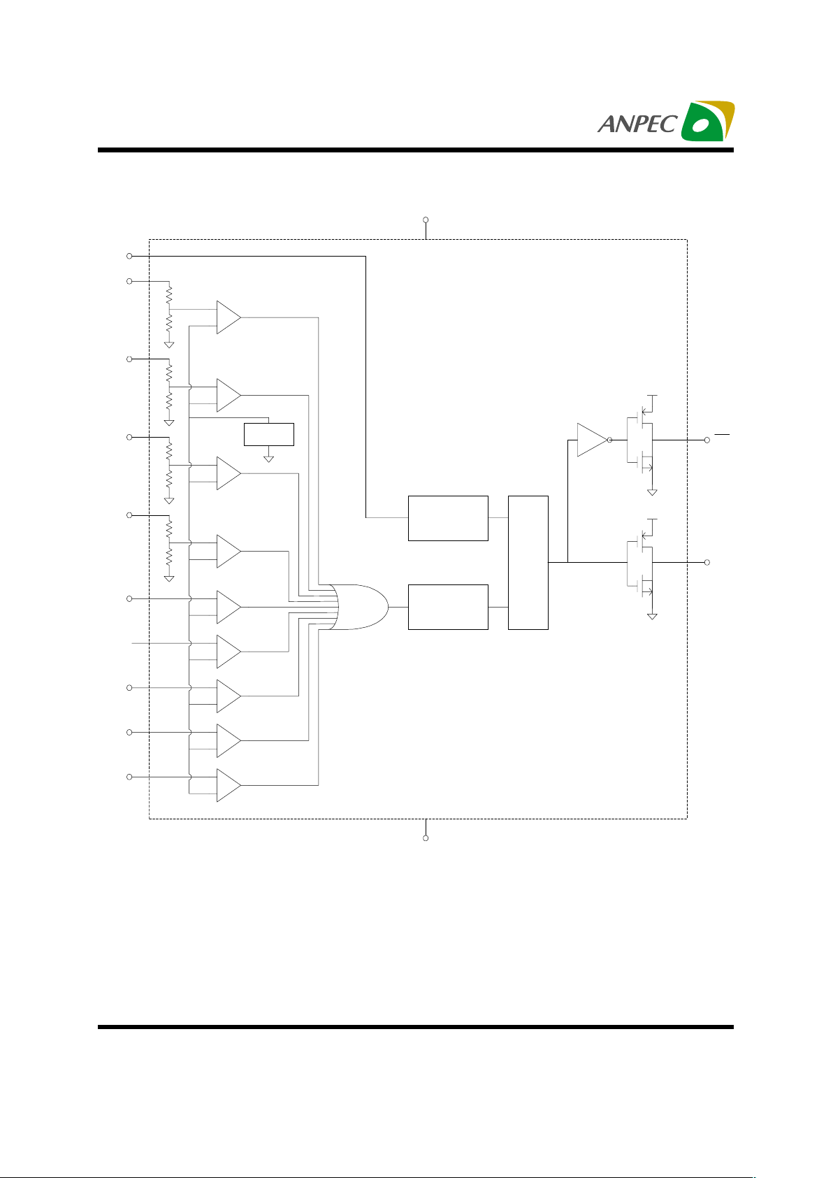
Block Diagram
_
+
_
+
_
+
_
+
_
+
_
+
_
+
_
+
_
+
Vref=1.5V
POR
DebounceOR
Latch
Vcc
Vcc
CMP1
CMP2
CMP3
CMP4
CMP5
CMP6
CMP7
CMP8
CMP9
IN1
(7V)
IN2
(4.5V)
IN3
(4V)
IN4
(3V)
IN5
IN6
IN7
IN8
IN9
RESE
T
Vout
Vout
GND
Vcc(2~3.3V)
 Loading...