

APW8824
1.5MHz, 1A Synchronous Buck Regulator
Features
• 1A Output Current
• Wide 2.7V~5.5V Input Voltage
• Fixed 1.5MHz Switching Frequency
• Low Dropout Operating at 100% duty cycle
• Low 25µA Quiescent Current
• Integrate Synchronous Rectifier
• 0.6V Low Reference Voltage
• <0.5µA Input Current during Shutdown
• Current-Mode Operation with Internal Compen-
sation
- Stable with Ceramic Output Capacitors
- Fast Line Transient Response
• Over-Voltage Protection
• Under Voltage Protection
• Over-Temperature Protection with Hysteresis
• Available in a TSOT-23-6A Package
• Halogen and Lead Free Available
(RoHS Compliant)
General Description
The APW8824 is a high efficiency monolithic synchronous buck regulator. APW8824 operates with a constant
1.5MHz switching frequenc y and using the inductor current as a controlled quantity in the current mode
architecture. The 2.7V to 5.5V input voltage range makes
the APW8824 ideally suited for single Li-Ion battery powered applications. 100% duty cycle provides low dropout
operation, extending battery life in portable electrical
devices. The internally fixed 1.5MHz operating frequency
allows the use of small surface mount inductors and
capacitors. The synchronous switches inc luded inside
increase the efficienc y and eliminate the need for an external Schottky diode.
The APW8824 is available in TSOT-23-6A package
Applications
• HD STB
• BT Mouse
• PND Instrument
• Portable Instrument
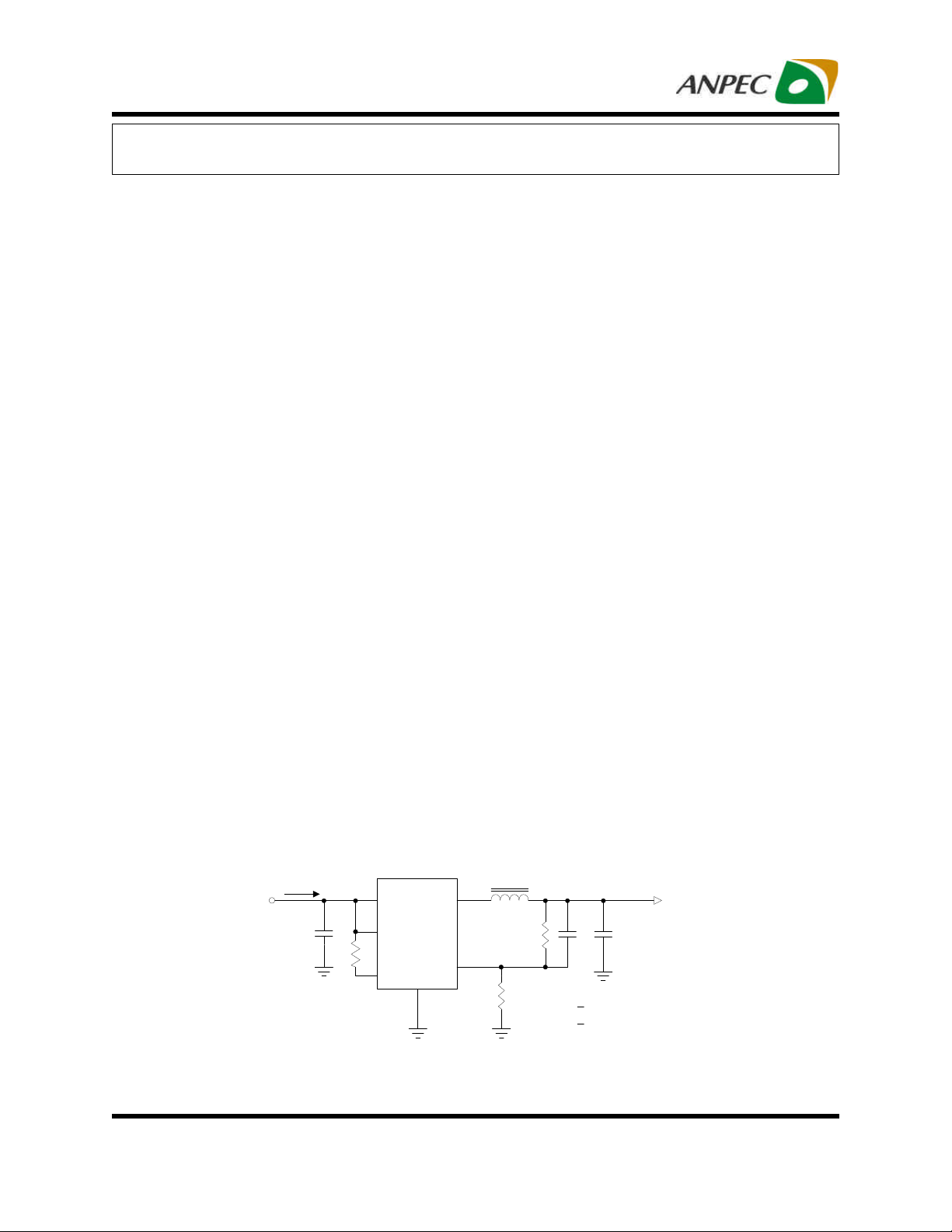
Simplified Application Circuit
L1
I
V
IN
IN
2.7~5.5V
ANPEC reserves the right to make changes to improve reliability or manufacturability without notice, and
advise customers to obtain the latest version of relevant information to verify before placing orders.
Copyright ANPEC Electronics Corp.
Rev. A.2 - May., 2013
C1
10µF
(MLCC)
R3
100k
4
VIN
1
5
EN
APW8824
PG
GND
LX
FB
2
2.2µH
3
R1
C3
6
R2
(option)
R1 < 1.5MΩ is recommended
R2 < 200KΩ is recommended
C2
10µF
(MLCC)
V
OUT
0.6V~V
0~1A
IN
www.anpec.com.tw1
APW8824
Ordering and Marking Information
APW8824
Assembly Material
Handling Code
Temperature Range
Package Code
APW8824 CT: X - Date Code
W24X
Package Code
CT : TSOT-23-6A
Operating Ambient Temperature Range
I : -40 to 85oC
Handling Code
TR : Tape & Reel
Assembly Material
G : Halogen and Lead Free Device
Note: ANPEC lead-free products contain molding compounds/die attach materials and 100% matte tin plate termination finish; which
are fully compliant with RoHS. ANPEC lead-free products meet or exceed the lead-free requirements of IPC/JEDEC J-STD-020D for
MSL classification at lead-free peak reflow temperature. ANPEC defines “Green” to mean lead-free (RoHS compliant) and halogen
free (Br or Cl does not exceed 900ppm by weight in homogeneous material and total of Br and Cl does not exceed 1500ppm by
weight).
Pin Configuration
APW8824
EN 1
GND 2
LX 3
TSOT-23-6A Top View
6 FB
5 PG
4 VIN
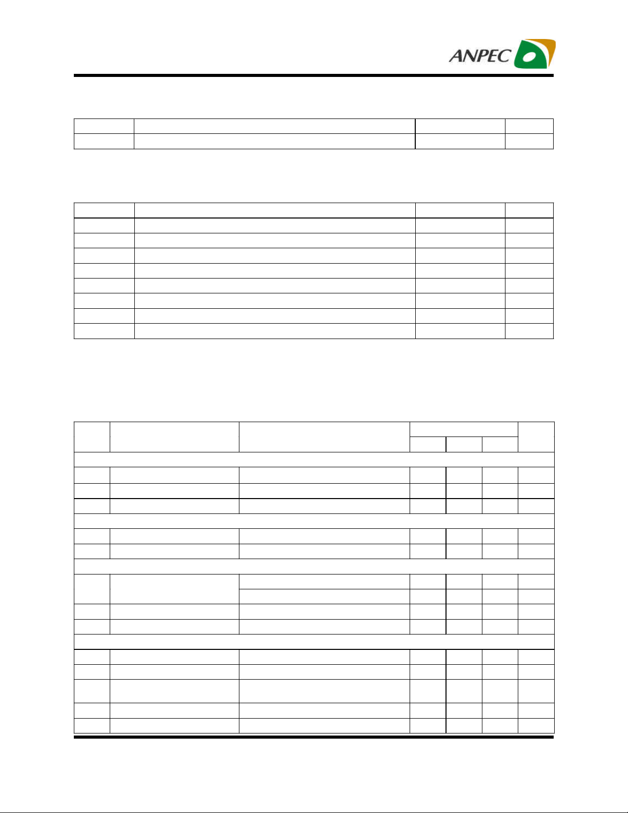
Absolute Maximum Ratings (Note 1)
Symbol Parameter Rating Unit
VIN Input Bias Supply Voltage (VIN to GND) -0.3 ~ 7 V
VLX LX Voltage (LX to GND)
T
STG
T
SDR
Note 1: Stresses beyond those listed under “Absolute Maximum Ratings” may cause permanent damage to the device. These are
stress ratings only and functional operation of the device at these or any other conditions beyond those indicated in the operational
sections of the specifications is not implied. Exposure to absolute maximum rating conditions for extended periods may affect device
reliability.
Copyright ANPEC Electronics Corp.
Rev. A.2 - May., 2013
EN, FB, LX and PG to GND Voltage
Maximum Junction Temperature
Storage Temperature
Maximum Lead Soldering Temperature (10 Seconds)
<30ns pulse width
>30ns pulse width
-0.3 ~ VIN+0.3 V
-3 ~ 8
-0.3 ~ VIN +0.3
150
-65 ~ 150
260
www.anpec.com.tw2
V
o
C
o
C
o
C
APW8824
Thermal Characteristics
Symbol Parameter Typical Value Unit
θJA
Note 2: θJA is measured with the component mounted on a high effective thermal conductivity test board in free air.
Recommended Operating Conditions (Note 3)
Symbol Parameter Range Unit
VIN Input Bias Supply Voltage (VIN to GND) 2.7 ~ 5.5 V
V
OUT
I
OUT
L1
CIN
C
OUT
TA
TJ
Junction-to-Ambient Resistance in free air (Note 2) 220
Converter Output Voltage 0.6 ~ VIN V
Converter Output Current 0 ~ 1 A
Converter Output Inductor
Converter Input Capacitor
Converter Output Capacitor
Ambient Temperature
Junction Temperature
1.0 ~ 10
10 ~ 100
10 ~ 100
-40 ~ 85
-40 ~ 125
o
C/W
µH
µF
µF
o
o
C
C
Note 3: Refer to the application circ uit for further information
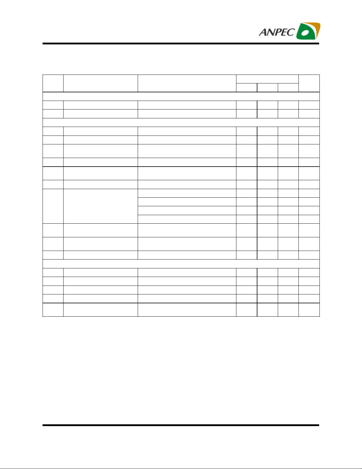
Electrical Characteristics
Unless otherwise specified, these specifications apply over VIN=3.6V and TA= -40 ~ 85 oC. Typical values are at TA=25oC.
Symbol
Parameter Test Conditions
SUPPLY VOLTAGE AND CURRENT
VIN Input Voltage Range
IDD Quiescent Current VFB = 0.66V - 25 40
ISD Shutdown Input Current EN = GND - - 0.5
POWER-ON-RESET (POR) and LOCKOUT VOLTAGE THRESHOLDS
UVLO Threshold 2.1 2.35 2.6 V
UVLO Hysteresis - 0.1 - V
REFERENCE VOLTAGE
V
Reference Voltage
REF
Output Voltage Accuracy 0A < I
IFB FB Input Current
TA = 25 oC 0.594 0.6 0.606
TA = -40~85 oC, TJ = -40~125 oC 0.591
< 1A, VIN > 3.6V, TJ =25 oC -1.5 - +1.5 %
OUT
INTERNAL POWER MOSFETS
FSW Switching Frequency VFB = 0.6V 1.2 1.5 1.8 MHz
R
R
Main Switch ON Resistance ILX=200mA - 0.28 0.35
P-FET
Synchronous Switch ON
N-FET
Resistance
N-FET Switch Leakage Current V
P-FET Switch Leakage Current V
ILX=200mA - 0.25 0.32
= GND, VLX = 5V -0.1 - 0.1
RUN
= GND, V
RUN
= 0V -0.1 - 0.1
LX
Copyright ANPEC Electronics Corp.
Rev. A.2 - May., 2013
APW8824
Min Typ Max
2.7 - 5.5
- 0.609
-50 - 50 nA
www.anpec.com.tw3
Unit
V
µA
µA
V
V
Ω
Ω
µA
µA
APW8824
Electrical Characteristics
Unless otherwise specified, these specifications apply over VIN=3.6V and TA= -40 ~ 85 oC. Typical values are at TA=25oC.
Symbol
Parameter Test Conditions
APW8824
Min Typ Max
INTERNAL POWER MOSFETS
Dead-time (Note 4) - 5 - ns
Duty Cycle 0 - 100 %
PROTECTION
I
I
Maximum Inductor Current Limit
LIM
N-FET Negative Current Limit - 1 - A
Over Voltage Protection
V
OVP
Threshold
, 2.7V≦VIN≦6V
P-FET
2 2.5 3 A
115 120 125 %V
OVP Debounce Time - 20 -
Under Voltage Protection
V
UVP
Threshold
57 66 75 %V
UVP Debounce Time - 15 -
PG in from Lower (PG Goes High) 87 90 93 %V
PG Threshold
PG Low Hysteresis (PG Goes Low) - 3 - %V
PG in from Higher (PG Goes High) 115 120 125 %V
PG High Hysteresis (PG Goes Low) - 3 - %V
PG High to Low debounce time
(V
under shoot)
OUT
PG High to Low debounce time
(V
over shoot)
OUT
T
Over-Temperature Protection TJ Rising - 150 - °C
OTP
- 60 -
- 80 -
START-UP AND SHUTDOWN
TSS Soft-start Duration (Note 4) - 0.7 - ms
EN Input High Threshold VIN = 2.7V~5.5V - - 1.5 V
EN Input Low Threshold VIN = 2.7V~5.5V 0.4 - - V
EN Leakage Current VEN = 5V, VIN = 5V -1 - 1
Power Good Pull Low
Resistance
Note 4: Guaranteed by design, not production tested.
- 200 -
Unit
REF
µs
REF
µs
REF
REF
REF
REF
µs
µs
µA
Ω
Copyright ANPEC Electronics Corp.
www.anpec.com.tw4
Rev. A.2 - May., 2013
APW8824
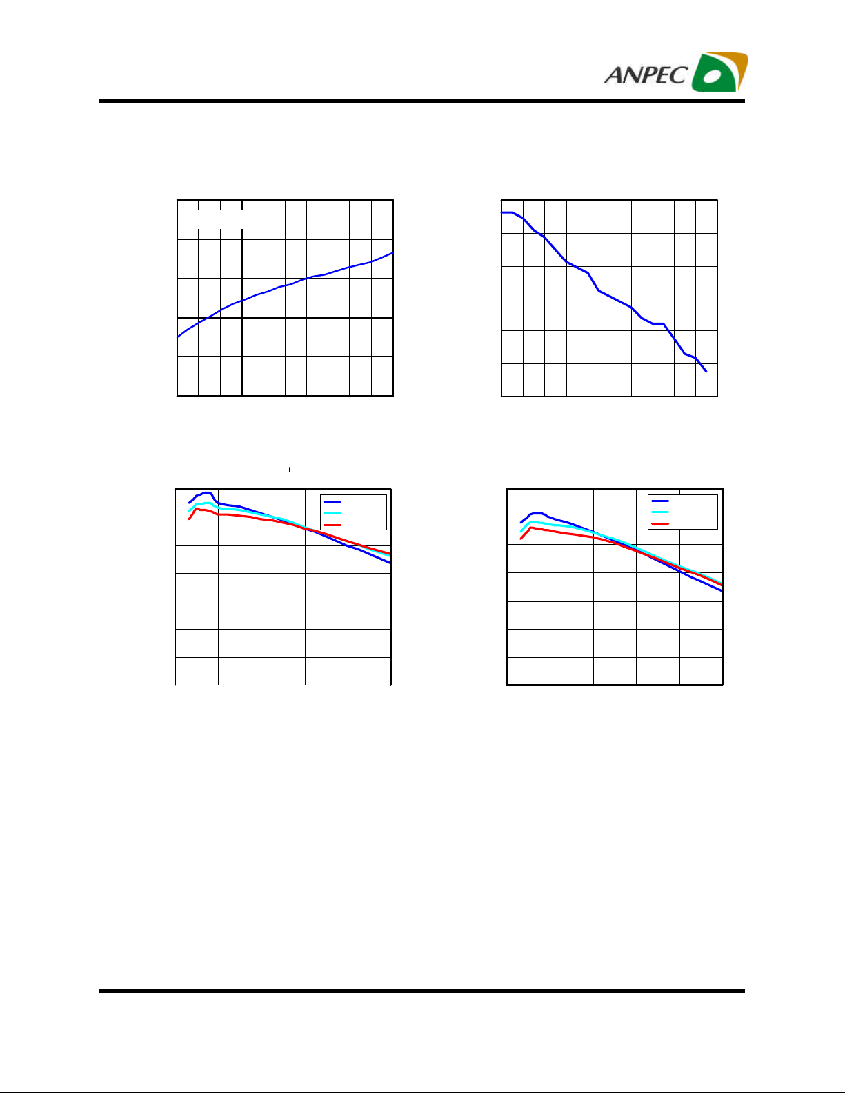
Typical Operating Characteristics
Output Voltage(V)
Output Voltage vs.
Temperature
1.525
Vout=1.5V
1.515
1.505
1.495
1.485
1.475
-40 -20 0 20 40 60 80 100 120 140 160
Temperature(oC)
Efficiency vs. Load Current
95
90
85
FSW=1.5MHz, V
OUT
=1.8V
VIN=3.3V
VIN=4.2V
VIN=5V
Switching Frequency vs
Temperature
1.6
1.55
1.5
1.45
1.4
Switching Frequency(MHz)
1.35
1.3
-40 -20 0 20 40 60 80 100 120 140 160
Temperature(oC)
Efficiency vs. Load Current
95
90
85
FSW=1.5MHz, V
OUT
=1.2V
VIN=3.3V
VIN=4.2V
VIN=5V
80
75
Efficiency (%)
70
65
60
0 0.2 0.4
0.6
Output Current (A)
0.8 1
80
75
Efficiency (%)
70
65
60
0 0.2 0.4 0.6 0.8 1
Output Current (A)
Copyright ANPEC Electronics Corp.
Rev. A.2 - May., 2013
www.anpec.com.tw5
APW8824
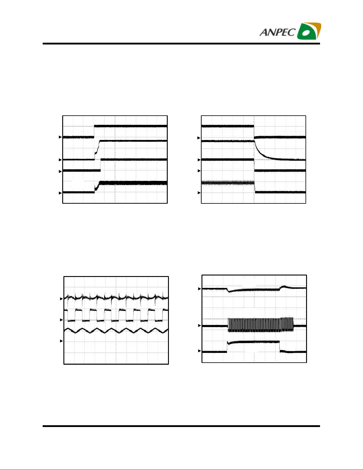
Operating Waveforms
Refer to the typical application circuit. The test condition is VIN=5V, TA= 25oC unless otherwis e specified.
1
2
3
I
L
4
CH1:VEN, 5V/Div
CH2:V
CH3:VPG , 5V/Div
CH3:IL, 1A/Div
TIME: 1ms/Div
OUT
, 1V/Div
Output Ripple
Enable
Shutdown
V
EN
V
EN
V
OUT
V
PG
1
V
OUT
2
3
4
I
L
V
PG
CH1: VEN, 5V/Div
CH2: V
CH3: V
CH4: IL, 1A/Div
OUT,
PG
1V/Div
5V/Div
TIME: 20µs/Div
Load Transient
V
OUT
1
V
LX
2
I
CH1: V
CH2: V
L
, 20mV/Div,AC
OUT
, 5V/Div
LX
3
CH3: IL , 1A/Div
TIME: 20µs/Div
Copyright ANPEC Electronics Corp.
Rev. A.2 - May., 2013
1
2
3
CH1: V
CH2: VLX,5V/Div
CH3: I
TIME: 100µs/Div
, 100mV/Div,AC
OUT
,1A/Div
OUT
V
OUT
V
LX
I
OUT
www.anpec.com.tw6
 Loading...