Anpec APW8822AQBI, APW8822BQBI, APW8822CQBI, APW8822QBI Schematics
APW8822/A/B/C
System Power PWM Controller for Notebook Computers with Charge Pump
Features
• Wide Input voltage Range from 6V to 25V
• Provide 5 Independent Outputs with ±1.0% Accu-
racy Over-Temperature
- PWM1 Controller with Adjustable (2V to 5.5V) Output
- PWM2 Controller with Adjustable (2V to 5.5V) Output
- 100mA Low Dropout Regulator (LDO5) with Fixed
5V Output
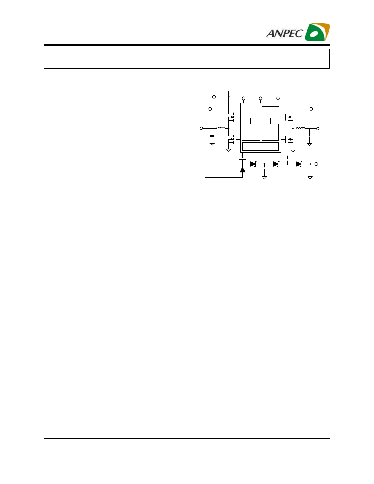
Simplified Application Circuit
C2
ENILIM2
LDO3
PWM2
C3
V
Q3
V
OUT2
L2
Q4
D4D3D2
V
C4
V
IN
6V~25V
V
LDO5
V
OUT1
L1
Q1
Q2
ENILIM1
LDO5
PWM1
Charge Pump
C1
D1
EN LDO
LDO3
CP
- 100mA Low Dropout Regulator (LDO3) with Fixed
3.3V Output
- 270kHz Clock Signal for 15V Charge Pump (Used
VOUT1 as Its Power Supply)
• Excellent Line/Load Regulations about ±1.5% Over-
Temperature Range
• Built in POR Control Scheme Implemented
• Constant On-Time Control Scheme with Frequency
Compensation for PWM Mode
• Selectable Switching Frequency in PWM Mode
• Built-in Digital Soft-Start for PWM Outputs and Soft-
Stop for PWM Outputs and LDO Outputs
• Integrated Bootstrap Forward P-CH MOSFET
• High Efficiency over Light to Full Load Range
(PWMs)
• Built-in Power Good Indicators (PWMs)
• Independent Enable Inputs (PWMs, LDO)
• 70% Under-Voltage and 125% Over-Voltage Protec-
tions (PWM)
• Adjustable Current-Limit Protection (PWMs)
- Using Sense Low-Side MOSFET’s R
DS(ON)
• Over-Temperature Protection
• 3mmx3mm Thin QFN-20 (TQFN3x3-20) package
• Lead Free and Green Device Available (RoHS
Compliant)
General Description
The APW8822/A/B/C integrates dual step-down, constanton-time, synchronous PWM controllers (that drives dual
N-channel MOSFETs for each channel) and two low dropout regulators as well as various protections into a chip.
The PWM controllers step down high voltage of a battery
to generate low-voltage for NB applications. The output
of PWM1 and PWM2 can be adjusted from 2V to 5.5V by
setting a resistive voltage-divider from VOUTx to GND.
The linear regulators provide 5V and 3.3V output for
standby power supply. The linear regulators provide up
to 100mA output current. When the PWMx output voltage
is higher than LDOx bypass threshold, the related LDOx
regulator is shut off and its output is connected to VOUTx
by internal switchover MOSFET. It can save power
dissipation. The charge pump circuit with 270kHz clock
driver uses VOUT1 as its power supply to generate approximately 15V DC voltage.
The APW8822/A/B/C provides excellent transient
response and accurate DC output voltage in either PFM
or PWM Mode. In Pulse-Frequency Mode (PFM), the
APW8822/A/B/C provides very high efficiency over light
to heavy loads with loading-modulated switching
frequencies. The Forced-PWM Mode works nearly at
constant frequency for low-noise requirements. The
unique ultrasonic mode maintains the switching
frequency above 25kHz, which eliminates noise in
audio application.
ANPEC reserves the right to make changes to improve reliability or manufacturability without notice, and
advise customers to obtain the latest version of relevant information to verify before placing orders.
Copyright ANPEC Electronics Corp.
Rev. A.2 - Nov., 2012
www.anpec.com.tw1
APW8822/A/B/C
General Description (Cont.)
The APW8822/A/B/C is equipped with accurate sourcing and current-limit, output under-voltage output overvoltage protections, being perfect for NB applications. A
1.4ms (typ.) digital soft-start can reduce the start-up
current. A soft-stop function actively discharges the
output capacitors by the discharge device. The
APW8822/A/B has individual enable controls for each
PWM channels. Pulling both EN1/2 pin low shuts down
the all of outputs unless LDO3 output. The LDO3 and
LDO5 of APW8822A/C are always on standby power.
The APW8822/A/B/C is available in a TQFN3x3-20
package.
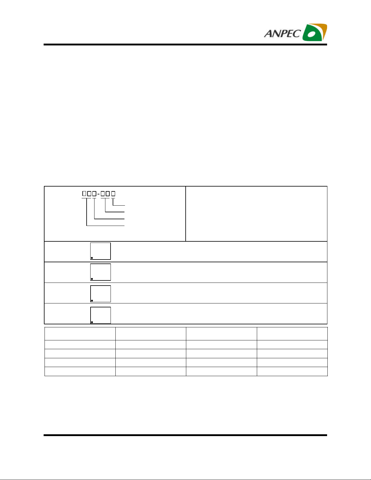
Ordering and Marking Information
APW8822
APW8822A
APW8822B
APW8822C
Assembly Material
Handling Code
Temperature Range
Package Code
Applications
• Notebook and Sub-Notebook Computers
• Portable Devices
• DDR1, DDR2, and DDR3 Power Supplies
• 3-Cell and 4-Cell Li+ Battery-Powered Devices
• Graphic Cards
• Game Consoles
• Telecommunications
Package Code
QB: TQFN 3 x3-20
Operating Ambient Temperature Range
I : -40 to 85 C
Handling Code
TR : Tape & Reel
Lead Free Code
L : Lead Free Device
°
G : Halogen and Lead Free Device
APW
APW8822 QB :
APW8822A QB :
APW8822B QB :
APW8822C QB :
DEVICE NUMBER ENABLE FUNCTION SKIP MODE ALWAYS ON-LDO
APW8822QBI EN1/EN2 Auto-skip LDO3
APW8822AQBI ENLDO/ENILIM1/ENILIM2 Auto-skip LDO3 & LDO5
APW8822BQBI EN1/EN2 Ultra-sonic LDO3
APW8822CQBI EN1/EN2 Auto-skip LDO3 & LDO5
Note: ANPEC lead-free products contain molding compounds/die attach materials and 100% matte tin plate termination finish; which
are fully compliant with RoHS. ANPEC lead-free products meet or exceed the lead-free requirements of IPC/JEDEC J-STD-020D for
MSL classification at lead-free peak reflow temperature. ANPEC defines “Green” to mean lead-free (RoHS compliant) and halogen
free (Br or Cl does not exceed 900ppm by weight in homogeneous material and total of Br and Cl does not exceed 1500ppm by
weight).
8822
XXXXX
APW
8822A
XXXXX
APW
8822B
XXXXX
APW
8822C
XXXXX
XXXXX - Date Code
XXXXX - Date Code
XXXXX - Date Code
XXXXX - Date Code
Copyright ANPEC Electronics Corp.
Rev. A.2 - Nov., 2012
www.anpec.com.tw2
APW8822/A/B/C
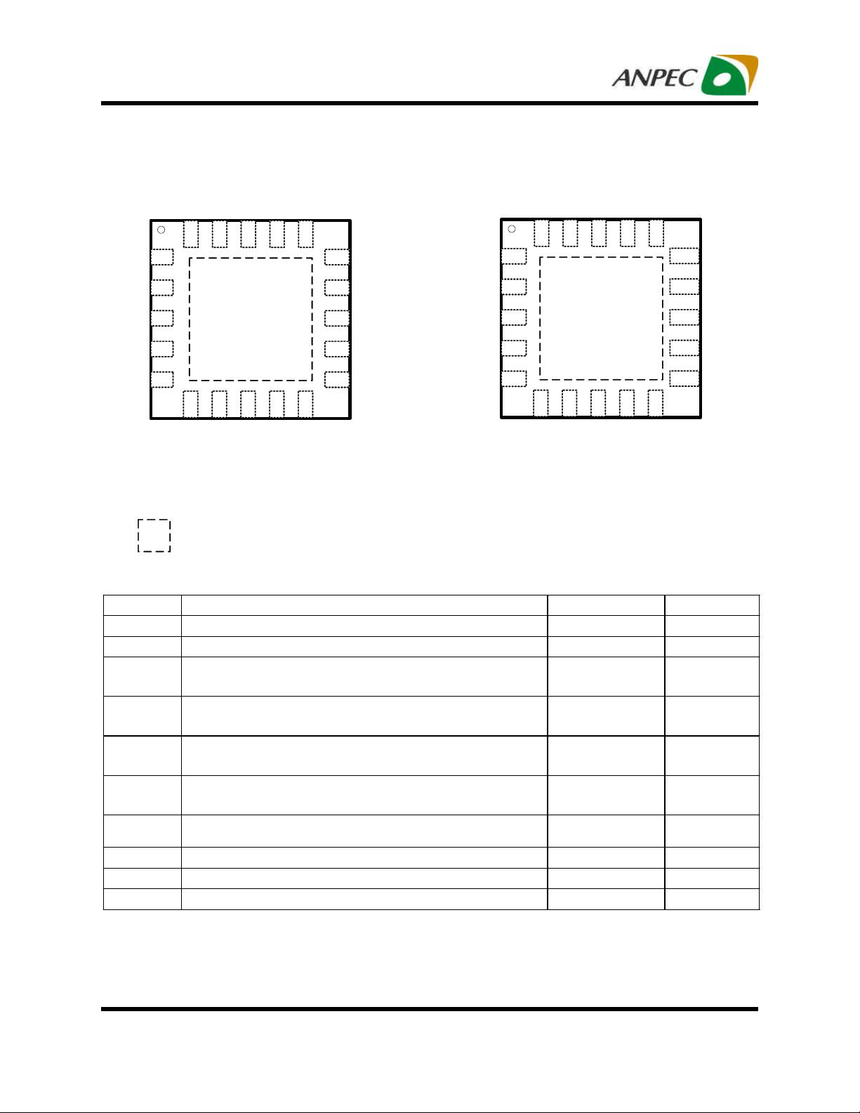
Pin Configuration
ENLDO
VCLK
PHASE1
BOOT1
UGATE1
17181920 16
LGATE1
1
2
3
Bottom View
APW8822A
15
14
13
BYP
LDO5
ILIM1
FB1
LDO3
EN1
VCLK
PHASE1
BOOT1
UGATE1
17181920 16
1
2
15
14
LGATE1
BYP
APW8822
3
Bottom View
APW8822B
13
LDO5
ENILIM1
FB1
LDO3
APW8822C
FB2
ILIM2
FB2
2
4
5
9876 10
NC
POK
BOOT2
PHASE2
TQFN 3X3-20
Top View
4
5
12
11
VIN
LGATE2
ENILIM
9876 10
EN2
POK
BOOT2
PHASE2
UGATE2
TQFN 3X3-20
Top View
12
VIN
LGATE2
11
UGATE2
= GND and Thermal Pad (connected to GND plane for better hat dissipation)
Absolute Maximum Ratings (Note 1)
Symbol Parameter Rating Unit
VIN Input Power Voltage (VIN to GND) -0.3 ~ 28 V
V
BOOT Supply Voltage (BOOT to PHASE) -0.3 ~ 7 V
BOOT
V
BOOT-GND
<20ns pulse width
>20ns pulse width
UGATE Voltage (UGATE to PHASE)
BOOT Supply Voltage (BOOT to GND)
V
UG-PHASE
<20ns pulse width
>20ns pulse width
LGATE Voltage (LGATE to GND)
V
LG-GND
<20ns pulse width
>20ns pulse width
PHASE Voltage (PHASE to GND)
V
PHASE
<20ns pulse width
>20ns pulse width
All Other Pins (LDOx, FBx, VOUTx, LDO5, LDO3, REF, VCLK, EN
LDO, ENILIMx to GND)
TJ Maximum Junction Temperature 150
T
Storage Temperature -65 ~ 150
STG
T
Maximum Lead Soldering Temperature, 10 Seconds 260
SDR
Note1: Stresses beyond those listed under "absolute maximum ratings" may cause permanent damage to the device. These are
stress ratings only and functional operation of the device at these or any other conditions beyond those indicated under "recommended operating conditions" is not implied. Exposure to absolute maximum rating conditions for extended periods may affect device
reliability.
-5 ~ 42
-0.3 ~ 35
-5 ~ V
-0.3 ~ V
-5 ~ V
-0.3 ~ V
BOOT
BOOT
LDO5
LDO5
+0.3
+0.3
+0.3
+0.3
-5 ~ 35
-0.3 ~ 28
-0.3 ~ 6 V
V
V
V
V
o
C
o
C
o
C
Copyright ANPEC Electronics Corp.
www.anpec.com.tw3
Rev. A.2 - Nov., 2012
APW8822/A/B/C
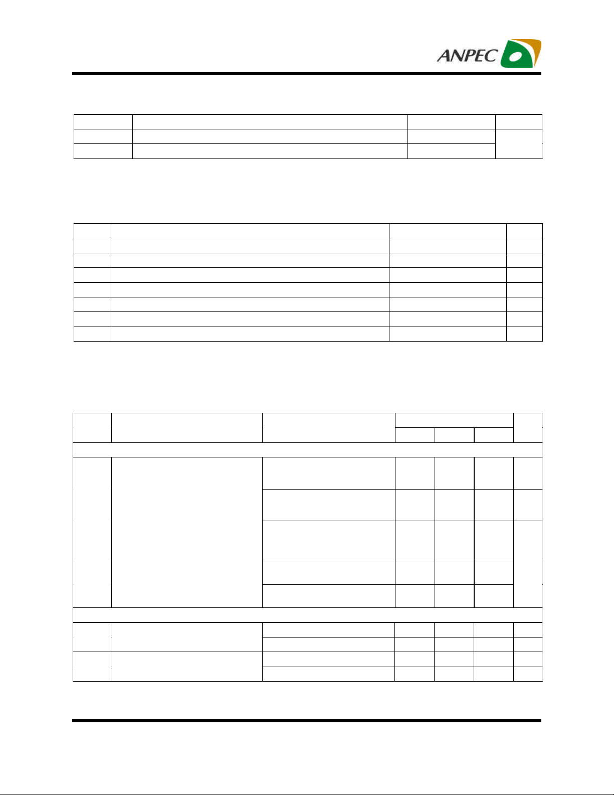
Thermal Characteristics (Note 2)
Symbol Parameter Typical Value Unit
θJA
θJC
Note 2: θJA is measured with the component mounted on a high effective thermal conductivity test board in free air. The thermal pad
of package is soldered directly on the PCB.
Recommended Operating Conditions
Thermal Resistance - Junction to Ambient 95
Thermal Resistance - Junction to Case 60
o
C/W
Symbol
Parameter Range Unit
VIN PWM1/2 Converter Input Voltage 6 ~ 25 V
V
V
PWM1 Converter Output Voltage 2 ~ 5.5 V
OUT1
PWM2 Converter Output Voltage 2 ~ 5.5 V
OUT2
CIN PWM1/2 Converter Input Capacitor (MLCC) 10 ~
C
LDO Output Capacitor (MLCC) 1.0 ~
LDO
TA Ambient Temperature -40 ~ 85
TJ Junction Temperature -40 ~ 125
µF
µF
o
C
o
C
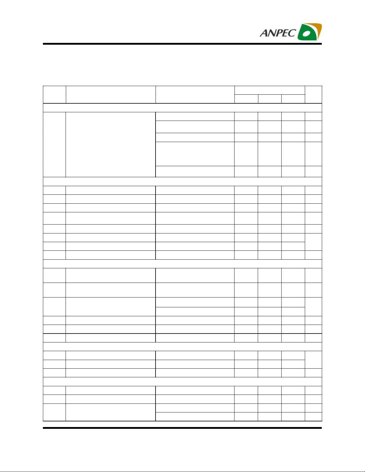
Electrical Characteristics
Refer to the typical application circuits. These specifications apply over VIN=12V and TA= -40 ~ 85 °C, unless otherwise
specified. Typical values are at TA=25°C.
Symbol
INPUT SUPPLY POWER
VIN Supply Current
IVN
Parameter Test Conditions
Supply current1, VOUT1=0V,
EN1=EN2=5V, VFB1 = VFB2 = 2.05V
Supply current2, VOUT1=5V,
EN1=EN2=5V, V
P
VIN+PLDO5
FB1
= V
FB2
Standby current1, VOUT1=0V,
EN1=EN2=0V (For APW8822/B)
= 2.05V,
APW8822
Min. Typ. Max.
- 0.86 1.2 mA
- 5 7 mW
- - 80
Unit
Standby current2, VOUT1=0V,
EN1=EN2=0V (For APW8822A/C)
Shutdown current, ENLDO=0V,
ENILIMx=0V (For APW8822A)
- 180 245
- 20 40
µA
UNDER-VOLTAGE LOCK OUT PROTECTION (UVLO)
LDO5 UVLO threshold
LDO3 UVLO threshold
Rising Edge 4.1 4.2 4.3 V
Hysteresis - 0.1 - V
Rising Edge 3.0 3.15 3.3 V
Hysteresis - 0.8 - V
Copyright ANPEC Electronics Corp.
www.anpec.com.tw4
Rev. A.2 - Nov., 2012
APW8822/A/B/C
Falling threshold2, PWMx shutdown
Falling threshold1, LDOx shutdown
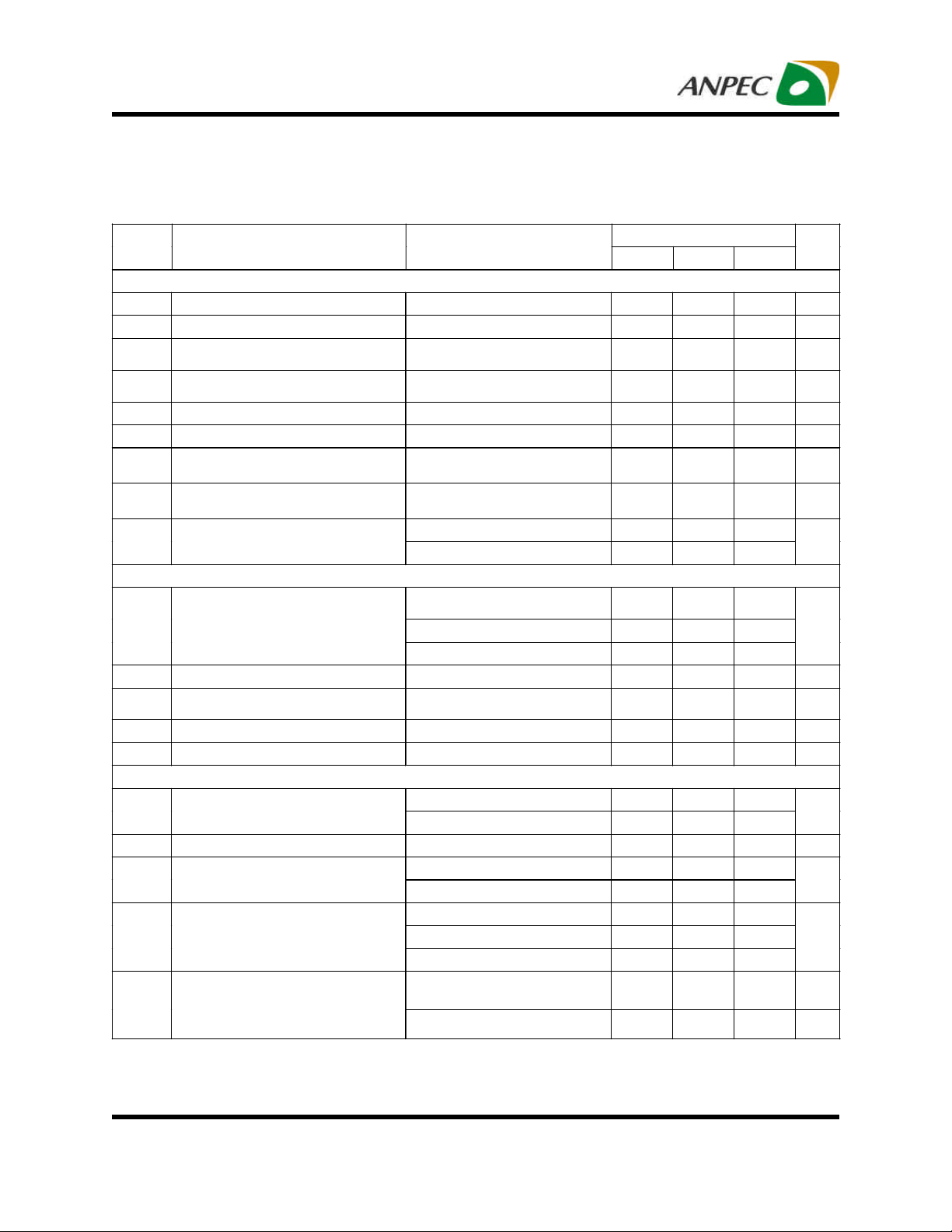
Electrical Characteristics
Refer to the typical application circuits. These specifications apply over VIN=12V and TA= -40 ~ 85 °C, unless otherwise
specified. Typical values are at TA=25°C.
Symbol
Parameter Test Conditions
UNDER-VOLTAGE LOCK OUT PROTECTION (UVLO)
Rising threshold1, LDO3 enable
Rising threshold1_A/C, LDO3 &
LDO5 enable (For APW8822A/C)
Rising threshold2, LDO5 enable
VIN POR threshold
with soft stop.
When PWMx soft stop is complete,
LDO5 will begin to shutdown
with soft stop
PWM CONTROLLERS
Output Voltage Adjust Range
VFB
TSS
F
F
FBx Reference Voltage
FBx input current
IFB
Soft-Start Ramp Time
Soft-Stop Time
PWM1 Switching Frequency
SW1
PWM2 Switching Frequency
SW2
UGATEx Minimum Off-Time
VOUT1, VOUT2
TA = -40 oC to 85 oC
V
ENx High to V
LDO5=5V
ENx low to V
VIN=20V, PWM1=5V 240
VIN=20V, PWM2=3.33V 280
LOW DROUPUT LINEAR REGULATORS (LDO5/LDO3)
V
THBYP5
LDO5 Output Voltage
LDO3 Output Voltage
LDO5 Bypass Threshold for
VOUT1-to-LDO5 Switch On
VOUT1-to-LDO5 Switch On Resistance
LDOx Current Limit
LDOx Discharge On Resistance
VOUT1=GND, 6V<VIN<25V,
0<I
VOUT2=GND, 6V<VIN<25V,
0<I
Hysteresis
VOUT1=5V, 50mA
VOUTx=GND, LDOx = GND
I
LDOX
CHARGE PUMP CLOCK
V
V
F
CLKH
CLKL
CLK
High level voltage
Low level voltage
Clock frequency
I
VCLK
I
VCLK
TA=25 oC
PWM1/2 PROTECTIONS
Over Voltage Protection Threshold
Over Voltage Fault Propagation Delay
Current Limit Current Source
V
Delta voltage=10mV
V
On the basis of 25 oC - 4500 -
Copyright ANPEC Electronics Corp.
Rev. A.2 - Nov., 2012
Min. Typ. Max.
- 3.8 - V
- 3.8 -
- 5.1 - V
- 5.0 - V
- 3.7 - V
2 - 5.5 V
1.98 2.0 2.02 V
=2.0V, TA=25 oC
FBX
FBX
95% Regulation,
OUT
<0.1V
-20 - 20 nA
- 1.4 - ms
- 1.7 - ms
200 350 500 ns
<100mA
LDO5
<100mA
LDO3
4.8
3.2
VOUT1 Regulation Voltage Rising 4.55
0.15
-
150
=5mA
=-10mA, LDO5=5V, TA=25 oC
=10mA, LDO5=5V, TA=25 oC
Rising
FBX
=1V, TA = 25 oC
ILIMx
- 50 100
- 4.92
0.06 -
- 270 - kHz
120 125 130 %
- 3 -
9 10 11
APW8822
300 360
355 430
5.0
3.33
4.7
0.25 0.3
1.5
250
www.anpec.com.tw5
5.2
3.46
4.85
3
350
-
Unit
V
kHz
V
V
V
Ω
mA
Ω
V
µs
µA
ppm/oC
APW8822/A/B/C
Electrical Characteristics (Cont.)
Refer to the typical application circuits. These specifications apply over VIN=12V and TA= -40 ~ 85 °C, unless otherwise
specified. Typical values are at TA=25°C.
Symbol
PWM1/2 PROTECTIONS
POWER GOOD
LOGIC LEVELS
ILIMx Adjustment Range
ENILIMx Adjustment Range
Maximum setting voltage
Current limit comparator offset
Zero-Crossing Threshold
Under-Voltage Protection Threshold
Under-Voltage Protection Debounce
Interval
Under-Voltage Protection Enable
Blanking Time
Over-Temperature Protection Threshold
POK Threshold
POK Propagation Delay
POK Enable Delay
POK Sink current
POK Leakage Current
ENx Input Voltage Level
Input leakage current
ENILIMx Input Voltage
ENLDO Input Voltage
ENLDO pin pull high function
Parameter Test Conditions
V
V
V
Threshpld
(V
V
V
From EN signal go high to SS_OK
TJ Rising - 160 -
Hysteresis - 25 -
POK in from Lower
(POK goes high)
POK hysteresis
POK in from higher (POK goes low) 120 125 130
From EN signal go high to POK go
High
V
V
Enable
Shutdown 0.6 - VEN=5V
Enable
Hysteresis - 60 Shutdown
Enable, VCLK=off 0.8 - 1.6
Enable, VCLK=on 2.4 - Short Current, ENLDO is short to
GND
Open Voltage, ENLDO is open(pull
high to internal regulator)
ILIMx-GND
ENILIMx-GND
ILIMx
ILIMx
PGND – PHASE
POK
POK
=5V, Setting Current Limit
ILIMx-GND-VPGND-PHASEx
=920mV
= 500mV
= 5V
),
APW8822
Min. Typ. Max.
0.2 - 2 V
0.515 - 2 V
205 250 - mV
-8
-5 0 5 mV
65 70 75 %
- 25 -
- 2 - ms
87 90 93
- 3 -
- 63 -
- 2 - ms
2.5 7.5 mA
- 0.1 1
- - 1.2
0.1 1
300 400 500
- - 0.4
- 1 -
2.4 3.34 - V
0
Unit
8 mV
µs
o
%
µs
µA
µA
mV
µA
C
V
V
Copyright ANPEC Electronics Corp.
Rev. A.2 - Nov., 2012
www.anpec.com.tw6
APW8822/A/B/C
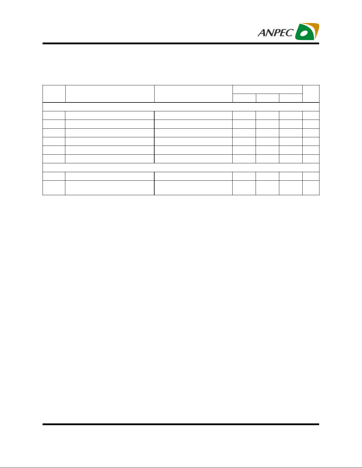
Electrical Characteristics (Cont.)
Refer to the typical application circuits. These specifications apply over VIN=12V and TA= -40 ~ 85 °C, unless otherwise
specified. Typical values are at TA=25°C.
Symbol
GATE DRIVERS
UG Pull-Up Resistance V
UG Sink Resistance V
LG Pull-Up Resistance V
LG Sink Resistance V
Dead Time UG falling to LG rising - 20 - ns
LG falling to UG rising - 20 -
BOOTSTRAP SWITCH
Forward Voltage
VF
Reverse Leakage
IR
Parameter Test Conditions
BOOTx
UGATEx
LDO5
LGATEx
V
LDO5
V
BOOTx-GND
V
LDO5
– V
– V
– V
– V
– V
= 5V
=250mV - 3 5
UGATEx
=250mV - 1.7 2.5
PHASEx
=250mV - 3 5
LGATEx
=250mV - 1 2
PGND
, IF = 10mA
BOOTx-GND
= 30V, V
PHASEx
= 25V,
APW8822
Min. Typ. Max.
- 0.4 0.5 V
- - 0.5
Unit
Ω
Ω
Ω
Ω
ns
µA
Copyright ANPEC Electronics Corp.
www.anpec.com.tw7
Rev. A.2 - Nov., 2012
APW8822/A/B/C
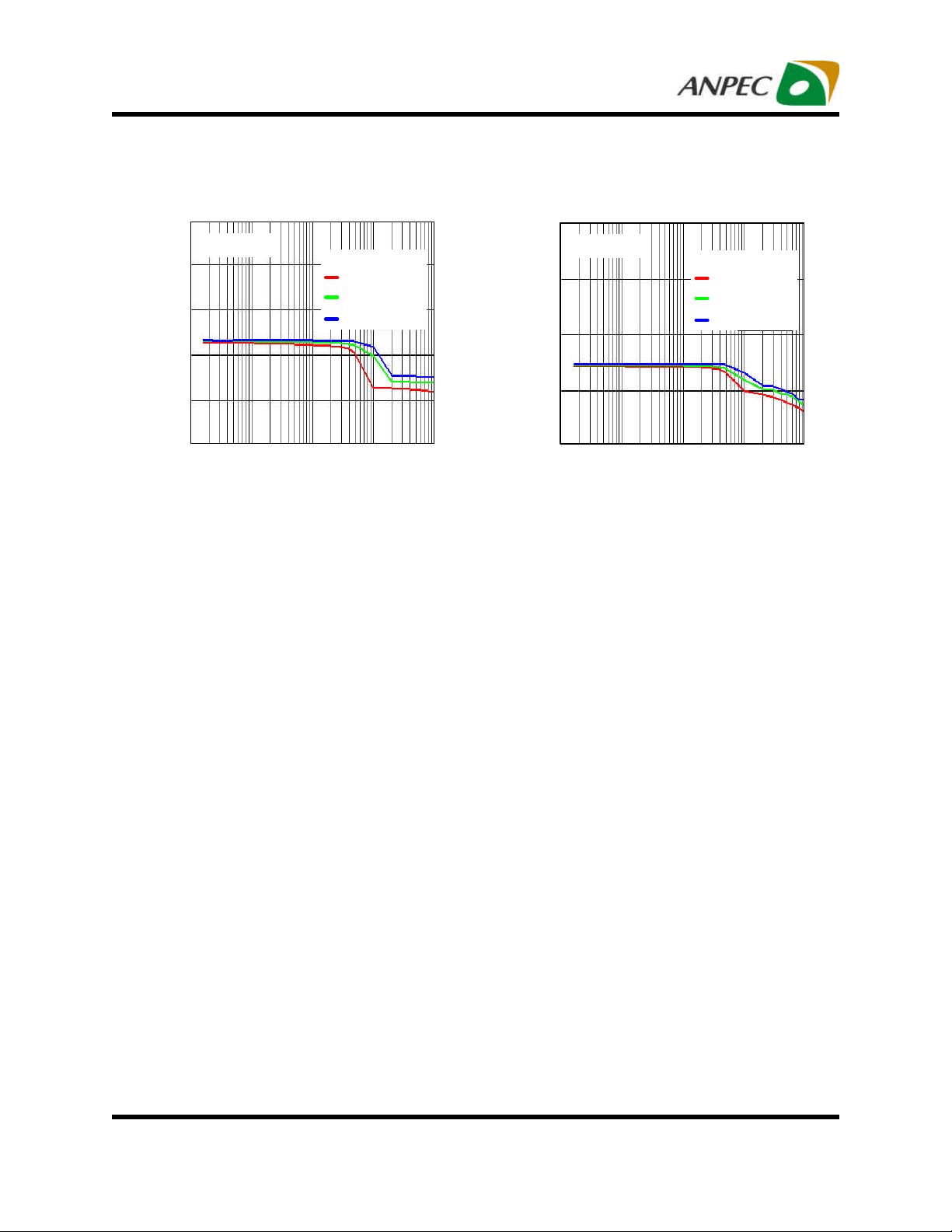
Typical Operating Characteristics
5.15
Load Regulation
Vout=5V
5.1
5.05
5
Outpur Voltage (V)
495
4.9
0.001 0.01 0.1 1
Output current(A)
VIN=8V
VIN=12V
VIN=20V
3.43
Load Regulation
Vout=3.3V
3.38
3.33
Outpur Voltage (V)
3.28
10
3.23
0.001 0.01 0.1 1
Output current(A)
VIN=8V
VIN=12V
VIN=20V
10
Copyright ANPEC Electronics Corp.
Rev. A.2 - Nov., 2012
www.anpec.com.tw8
APW8822/A/B/C
Operating Waveforms
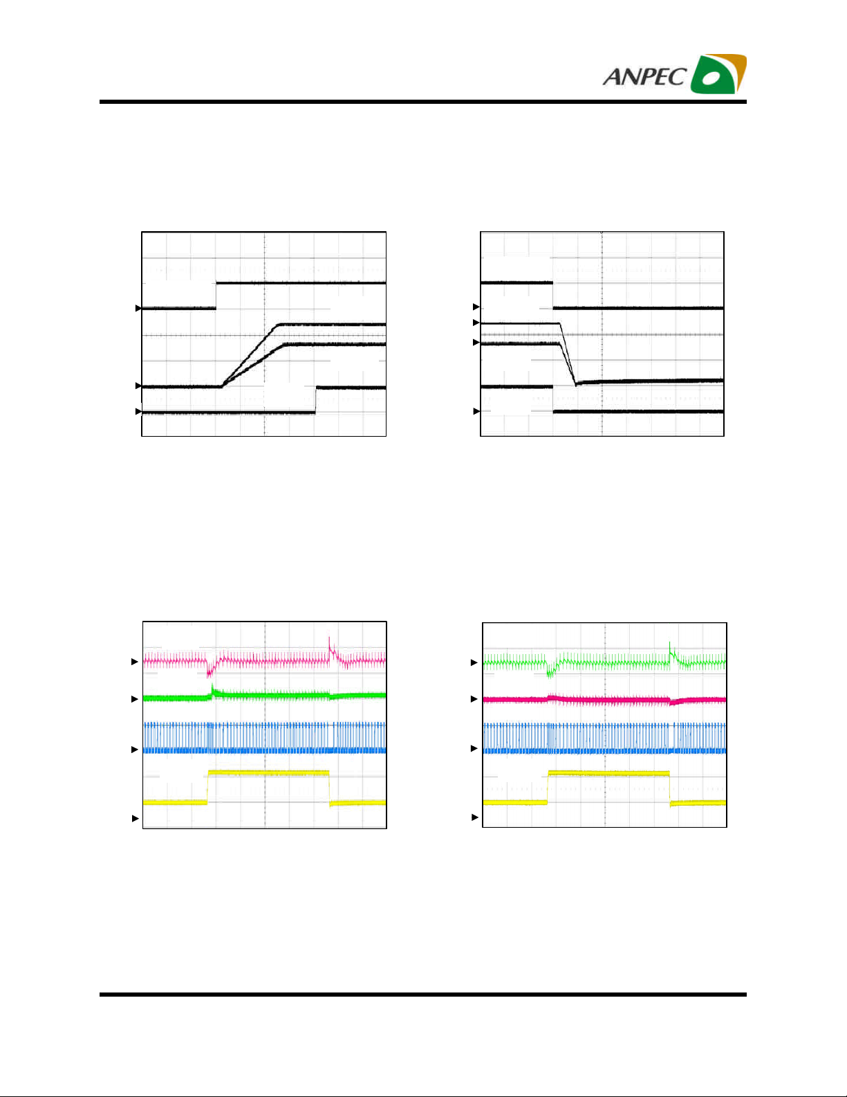
Refer to the typical application circuit. The test condition is VIN=12V, TA=25oC unless otherwise specified.
V
EN1=EN2
1
2
4
CH1: EN1=EN2, 5V/Div
CH2: V
CH3: V
CH4: V
OUT1
OUT2
, 10V/Div
POK
, 2V/Div
, 2V/Div
TIME: 500us/Div
Start-Up
V
POK
5V Load Transient
V
V
OUT1
OUT2
V
EN1=EN2
1
V
OUT1
2
3
V
OUT2
V
POK
4
CH1: EN1=EN2, 5V/Div
CH2: V
CH3: V
CH4: V
OUT1
OUT2
, 10V/Div
POK
, 2V/Div
, 2V/Div
TIME: 500us/Div
Output-Discharge
3.3V Load Transient
V
out1
1
V
OUT2
2
V
PHASE1
3
I
OUT1
4
CH1: Vout1, 100mV/Div, AC
CH2: Vout2, 100mV/Div, AC
CH3: V
CH4: I
PHASE1
OUT1
, 5A/Div
, 20V/Div, DC
TIME: 20us/Div
Copyright ANPEC Electronics Corp.
Rev. A.2 - Nov., 2012
V
out2
2
V
OUT1
1
V
PHASE2
3
I
OUT2
4
CH1: Vout1, 100mV/Div, AC
CH2: Vout2, 100mV/Div, AC
CH3: V
CH4: I
PHASE2
OUT2
, 5A/Div
, 20V/Div, DC
TIME: 20us/Div
www.anpec.com.tw9
 Loading...