
APW8819
DDR TOTAL POWER SOLUTION
SYNCHRONOUS BUCK CONTROLLER WITH 1.5A LDO
Features General Description
Buck Controller (VDDQ)
• High Input Voltages Range from 3V to 28V Input
Power
• Provide 1.8V (DDR2), 1.5V (DDR3) or Adjustable
Output Voltage from 0.5V to 2V
- ±1% Accuracy Over-Temperature
• Build in VREF Voltage 1.8V ±1% Accuracy over
Temperature
• Integrated MOSFET Drivers
• Integrated Bootstrap Forward P-CH MOSFET
• Excellent Line and Load Transient Responses
• PFM Mode for Increased Light Load Efficiency
• Selectable 300kHz/400kHz/500kHz Switching
Frequebcies
• Integrated MOSFET Drivers and Bootstrap Diode
• S3 and S5 Pins Control The Device in S0, S3, or
S4/S5 State
• Power Good Monitoring
• 50% Under-Voltage Protection (UVP)
• 125% Over-Voltage Protection (OVP)
• Adjustable Current-Limit Protection
- Using Sense Low-Side MOSFET R
DS(ON)
• QFN-20 3mmx3mm Package (QFN-20) and
QFN-16 3mmx3mm Thin Package (TQFN-16)
• Lead Free Available (RoHS Compliant)
+1.5A LDO Section (VTT)
• Souring or Sinking Current up to 1.5A
• Fast Transient Response for Output Voltage
• Output Ceramic Capacitors Support at Least
10µF MLCC
• VTT and VTTREF Track at Half the VDDQSNS by
Internal Divider
• ±20mV Accuracy for VTT and VTTREF
• Independent Over-Current-Limit (OCL)
• Thermal Shutdown Protection
The APW8819 integrates a synchronous buck PWM controller to generate VDDQ, a sourcing and sinking LDO
linear regulator to generate VTT. It provides a complete
power supply for DDR2 and DDR3 memory system. It
offers the lowest total solution cost in system where space
is at a premium.
The APW8819 provides excellent transient response and
accurate DC voltage output in PFM Mode. In Pulse Frequency Mode (PFM), the APW8819 provides very high efficiency over light to heavy loads with loading-modulated
switching frequencies.
The APW8819 is equipped with accurate current-limit,
output under-voltage, and output over-voltage protections.
A Power-On- Reset function monitors the voltage on VCC
prevents wrong operation during power on.
The LDO is designed to provide a regulated voltage with
bi-directional output current for DDR-SDRAM termination.
The device integrates two power transistors to source or
sink current up to 1.5A. It also incorporates current-limit
and thermal shutdown protection.
An internal resistor divider is used to provide a half voltage of VDDQSNS for VTTREF and VTT Voltage. The VTT
output voltage is only requiring 20µF of ceramic output
capacitance for stability and fast transient response. The
S3 and S5 pins provide the sleep state for VTT (S3 state)
and suspend state (S4/S5 state) for device, when S5 and
S3 are both pulled low the device provides the soft-off for
VTT and VTTREF.The APW8819 is available in
3mmx3mm 20-pin QFN and 3mmx3mm 16-pin TQFN
packages.
Applications
• DDR2, and DDR3 Memory Power Supplies
• SSTL-2 SSTL-18 and HSTL Termination
ANPEC reserves the right to make changes to improve reliability or manufacturability without notice, and
advise customers to obtain the latest version of relevant information to verify before placing orders.
Copyright ANPEC Electronics Corp.
Rev. A.6 - May, 2013
www.anpec.com.tw1
APW8819
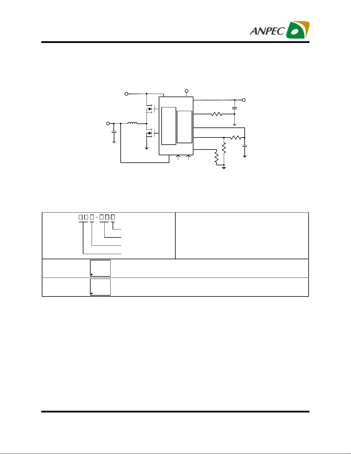
Simplified Application Circuit
V
IN
+3V~28V
Q1
VDDQ
L
OUT
Q2
PWM
S3
Ordering and Marking Information
APW8819
Assembly Material
Handling Code
Temperature Range
Package Code
APW
APW8819 QA :
8819
XXXXX
5V
VTT
VDDQ/2
R
OC
DDR
VREF
LDO
REFIN
R
MODE
R
MODE
TOP
R
GND
S5
Package Code
QA : QFN-20 QB : TQFN-16
Temperature Range
I : -40 to 85 oC
Handling Code
TR : Tape & Reel TY : Tray
Assembly Material
G : Halogen and Lead Free Device
XXXXX - Date Code
APW
APW8819 QB : XXXXX - Date Code
Note: ANPEC lead-free products contain molding compounds/die attach materials and 100% matte tin plate termination finish; which
are fully compliant with RoHS. ANPEC lead-free products meet or exceed the lead-free requirements of IPC/JEDEC J-STD-020D for
MSL classification at lead-free peak reflow temperature. ANPEC defines “Green” to mean lead-free (RoHS compliant) and halogen
free (Br or Cl does not exceed 900ppm by weight in homogeneous material and total of Br and Cl does not exceed 1500ppm by
weight).
Copyright ANPEC Electro nics Corp.
Rev. A.6 - May, 2013
8819
XXXXX
www.anpec.com.tw2
APW8819
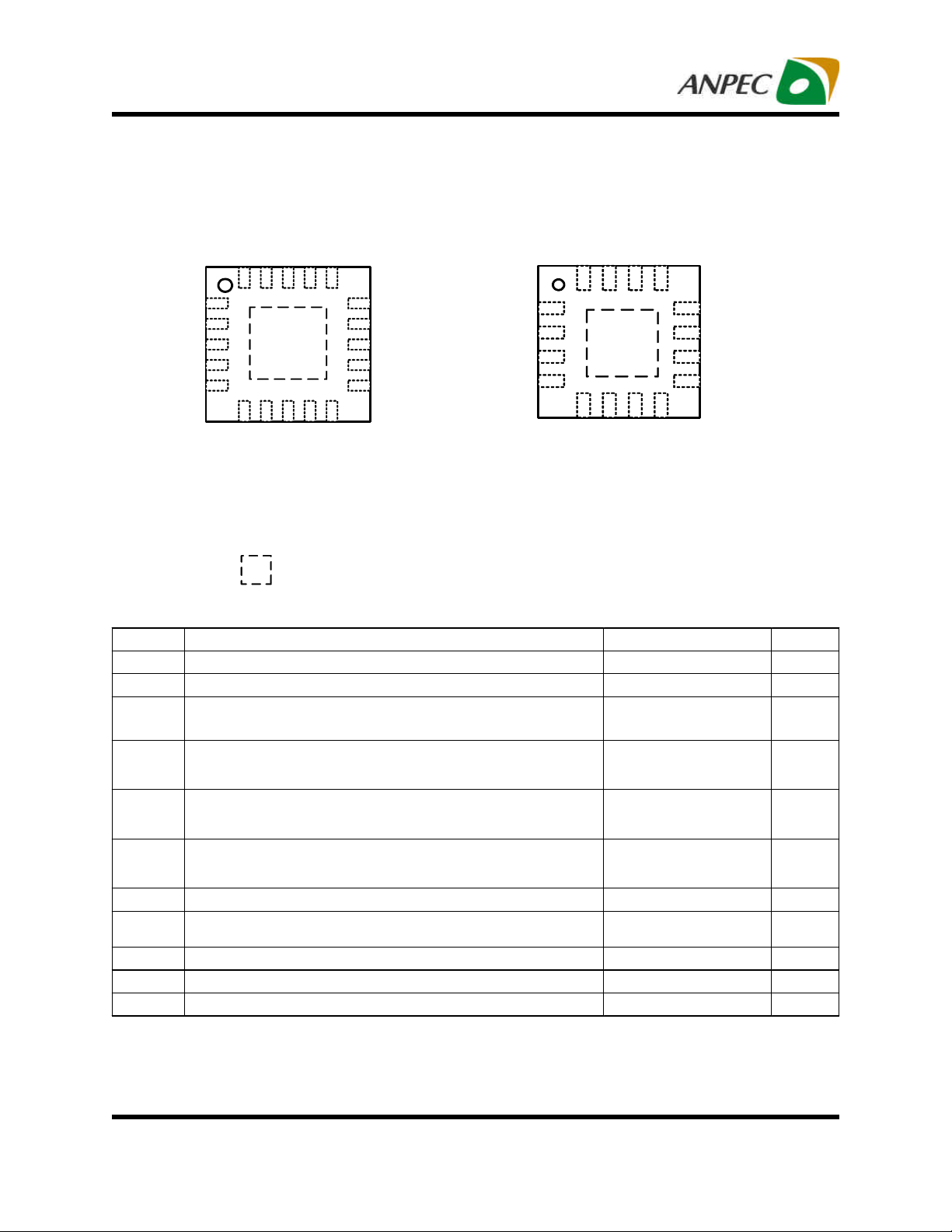
Pin Configuration
VTTSNS 1
VTT 3
VTTGND 4
VTTREF 5
MODE
POK
OC
S3
S5
20
19
7
6
VREF
GND
17
16
18
15 BOOT
14 UGATEVLDOIN 2
13 PHASE
12 VCC
11 LGATE
10
9
8
VDDQSNS
REFIN
PGND
POK 1
VLDOIN 2
VTT 3
VTTREF 4
QFN 3x3-20
(Top View)
= Thermal Pad (connected to GND plane for better heat dissipation)
MODE
OC
S3
16
15
14
GND
6
5
VREF
7
REFIN
VDDQSNS
TQFN 3x3-16
(Top View)
S5
13
12 BOOT
11 UGATE
10 PHASE
9 VCC
8
LGATE
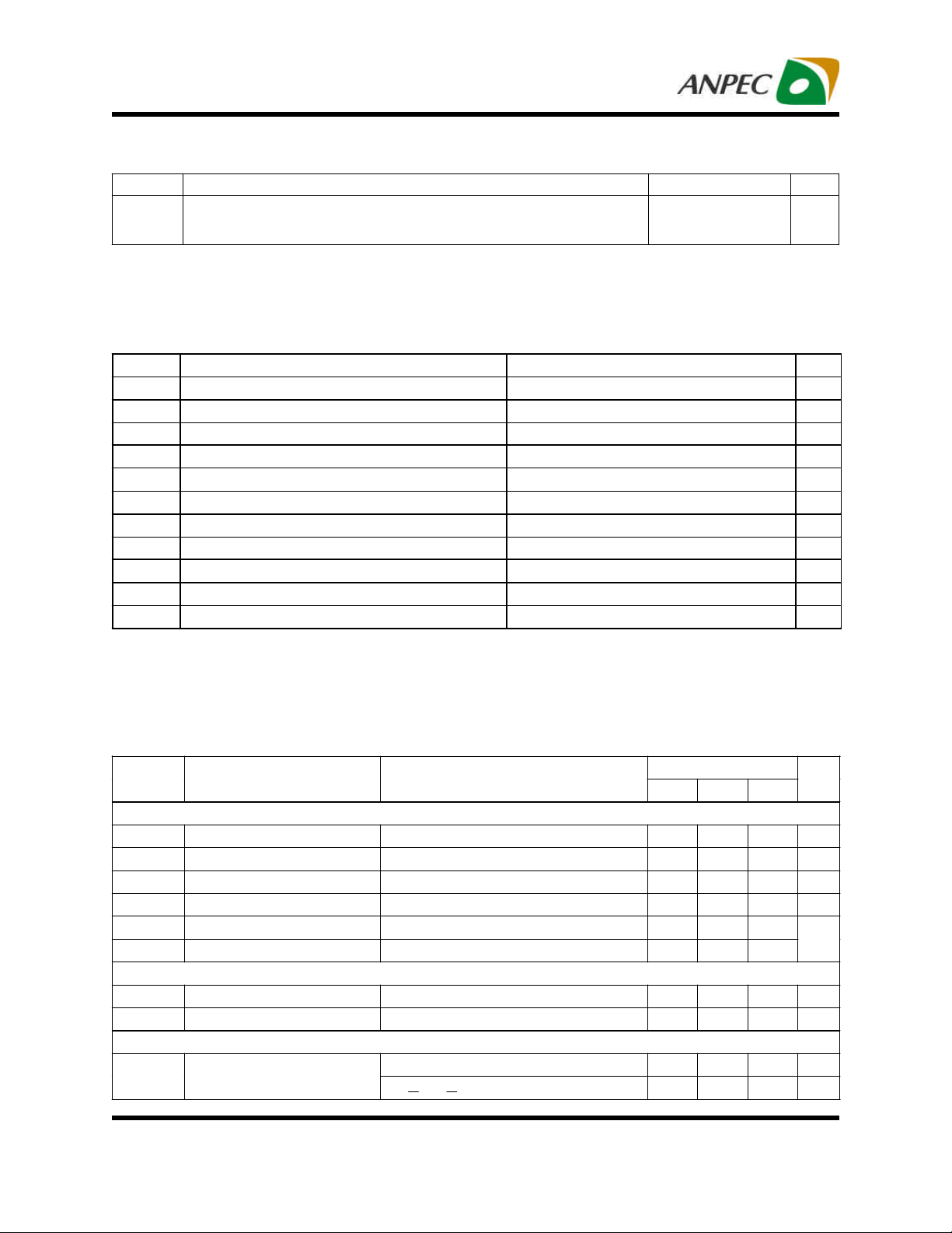
Absolute Maximum Ratings (Note 1, 2)
Symbol
VCC VCC Supply Voltage (VCC to GND) -0.3 ~ 7 V
V
BOOT Supply Voltage (BOOT to PHASE) -0.3 ~ 7 V
BOOT
BOOT Supply Voltage (BOOT to GND)
V
BOOT-GND
>20ns Pulse Width
UGATE Voltage (UGATE to PHASE)
<20ns Pulse Width
>20ns Pulse Width
LGATE Voltage (LGATE to GND)
<20ns Pulse Width
>20ns Pulse Width
PHASE Voltage (PHASE to GND)
<20ns Pulse Width
>20ns Pulse Width
PGND and VTTGND to GND Voltage -0.3 ~ 0.3 V
All Other Pins (OC, MODE, S3, S5, VDDQSNS, VTTSNS, VLDOIN,
VREF, POK, VTT, VTTREF and REFIN to GND Voltage)
TJ Maximum Junction Temperature 150
T
Storage Temperature -65 ~ 150
STG
T
Maximum Soldering Temperature, 10 Seconds 260
SDR
Note1: Stresses beyond those listed under "absolute maximum ratings" may cause permanent damage to the device. These are
stress ratings only and functional operation of the device at these or any other conditions beyond those indicated under "recommended operating conditions" is not implied. Exposure to absolute maximum rating conditions for extended periods may affect device
reliability
Note 2: The device is ESD sensitive. Handling precautions are recommended.
Parameter Rating Unit
<20ns Pulse Width
-5 ~ 42
V
-0.3 ~ 35
-5 ~ V
-0.3 ~ V
BOOT
BOOT
+0.3
+0.3
V
-5 ~ VCC+0.3
V
-0.3 ~ VCC+0.3
-5 ~ 35
V
-0.3 ~ 28
-0.3 ~ 7 V
o
C
o
C
o
C
Copyright ANPEC Electro nics Corp.
www.anpec.com.tw3
Rev. A.6 - May, 2013
APW8819
Thermal Characteristics (Note 3)
Symbol
Thermal Resistance - Junction to Ambient
θJA
Note 3: θJA is measured with the component mounted on a high effective the thermal conductivity test board in free air. The exposed
Parameter Typical Value Unit
QFN3x3-20
TQFN3x3-16
95
95
°C/W
pad of package is soldered directly on the PCB.
Recommended Operating Conditions (Note 4)
Symbol
VCC VCC Supply Voltage 4.5 ~ 5.5 V
VIN
Converter Input Voltage 3 ~ 28 V
V
Converter Output Voltage 0.5 ~2V/ DDR2 (1.8V)/ DDR3 (1.5V) V
VDDQ
V
LDO Output Voltage 0.25~ 1 V
VTT
I
Converter Output Current 0 ~ 20 A
OUT
I
LDO Output Current -1.5 ~ +1.5 A
VTT
C
VCC Capacitance 1~ µF
VCC
C
VTT Output Capacitance 10~
VTT
C
VTTREF Output Capacitance 0.22 ~ 2.2 µF
VTTREF
TA
Ambient Temperature -40 ~ 85
TJ
Junction Temperature -40 ~ 125
Parameter Range Unit
µF
o
C
o
C
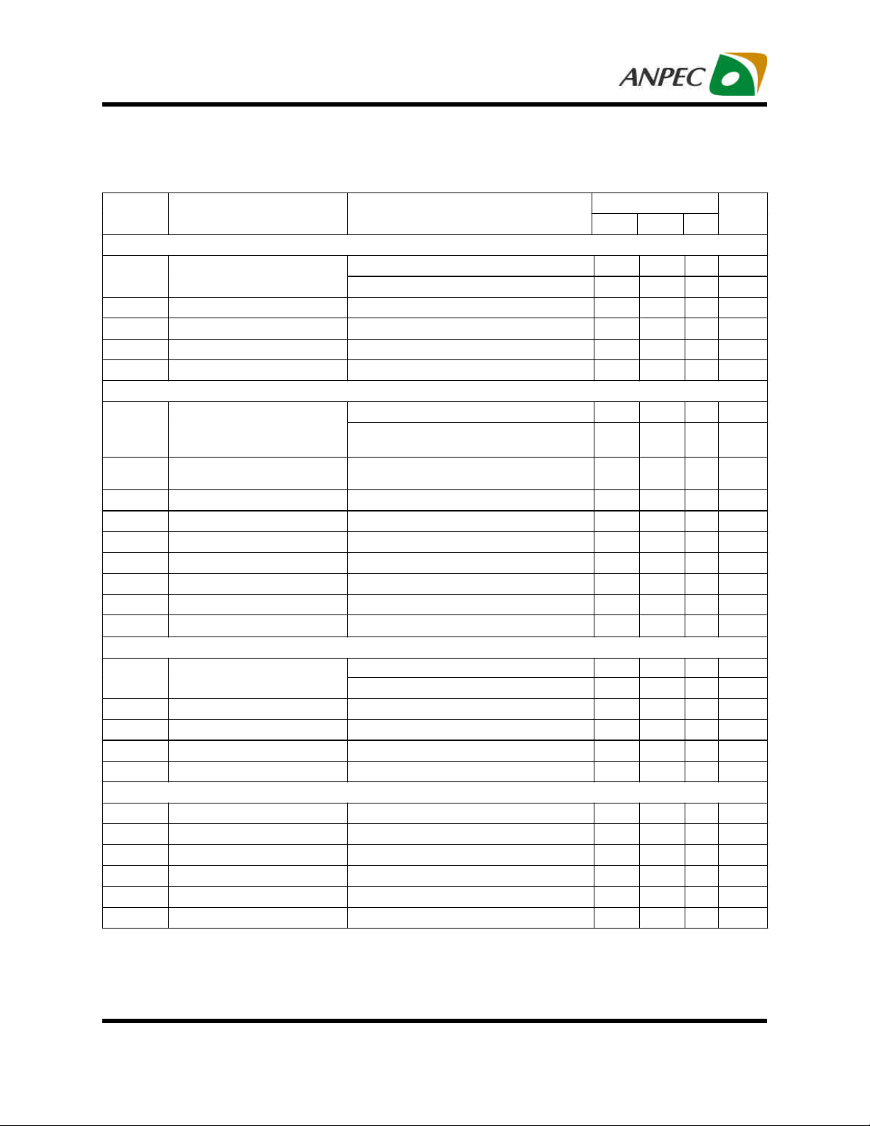
Electrical Characteristics
Refer to the typical application circuits. These specifications apply over V
VCC=VBOOT
otherwise s pecified. Typical values are at TA=25°C.
Symbol
Parameter Test Conditions
SUPPLY CURRENT
I
VCC Supply Current TA = 25oC, VS3 = VS5 = 5V, no load - 1.2 1.5 mA
VCC
I
VCC Standby Current TA = 25oC, VS3 = 0V, VS5 = 5V, no load - 740 850
VCCSTB
I
VCC Shutdown Current TA =25oC, VS3 = V
VCCSDN
I
LDOIN Supply Current TA = 25oC, VS3 = VS5 = 5V, no load 0.3 0.6 1 mA
LDOIN
I
LDOINSTB
I
LDOINSDN
LDOIN Standby Current TA = 25oC, VS3 = 0V, VS5 = 5V, no load - 0.1 10
LDOIN Shutdown Current TA = 25oC, VS3 = VS5 = 0V, no load - 0.1 1
= 0V, no load - 0.1 1
S5
POWER-ON-RESET
VCC POR Threshold VCC Rising 4.15 4.3 4.45 V
VCC POR Hysteresis - 100 - mV
VTT OUTPUT
I
=30µA, TA=25oC
V
VREF
VREF Output Voltage
VREF
0uA<I
<300uA, TA= -40oC~85oC
VREF
Copyright ANPEC Electro nics Corp.
Rev. A.6 - May, 2013
=5V, VIN=12V and TA= -40 ~ 85 °C, unless
APW8819
Min. Typ. Max.
- 1.8 - V
1.782
- 1.8144 V
www.anpec.com.tw4
Unit
µA
µA
µA
APW8819
µA
.5V, MODE Pin Pulled
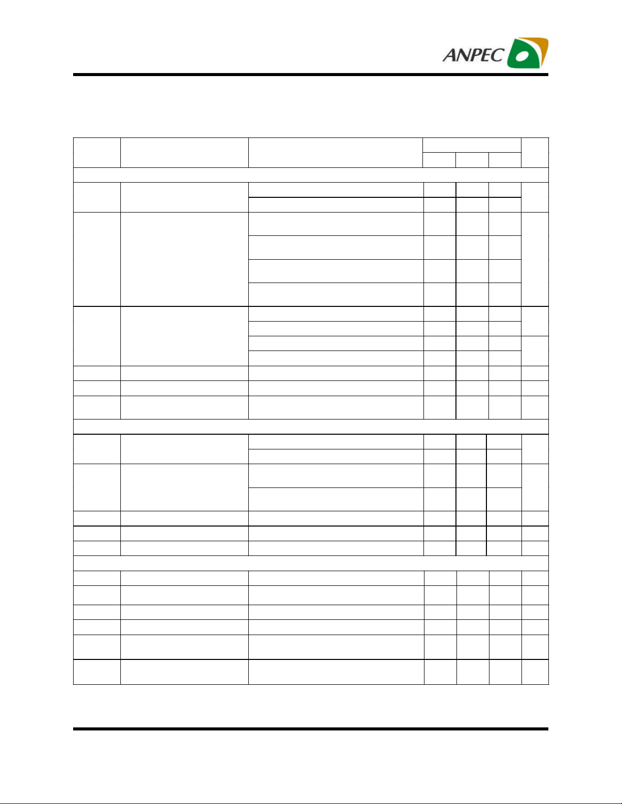
Electrical Characteristics (Cont.)
Refer to the typical application circuits. These specifications apply over V
otherwise s pecified. Typical values are at TA=25°C.
VCC=VBOOT
=5V, VIN=12V and TA= -40 ~ 85 °C, unless
Symbol
VTT OUTPUT
V
VTT Output Voltage
VTT
V
VTT Output Tolerance
VTT
I
Current-Limit
LIM
I
VTT Leakage Current V
VTTLK
I
VTTSNSLK
I
VTTDIS
VTTSNS Leakage Current V
VTT Discharge Current
VTTREF OUTPUT
V
VTTREF Output Voltage
VTTREF
VTTREF Tolerance
I
VTTREF Source Current V
VTTREF
I
VTTREF Sink Current V
VTTREF
I
VTTREFDIS
VTTREF Discharge Current TA = 25oC , S3=S5=0V, V
VDDQ OUTPUT
V
VDDQ Output Voltage V
VDDQ
VDDQSNS Regulation Voltage
Tolerance to REFIN
I
VDDQSNS
I
REFIN
VDDQSNS Input Current
REFIN Input Current
VDDQ Discharge Current
LDOIN Discharge Current
Parameter Test Conditions
V
= V
LDOIN
V
= V
LDOIN
V
= V
LDOIN
I
= 0A
VTT
V
= V
LDOIN
I
= 1.5A
VTT
V
= V
LDOIN
I
= 0A
VTT
V
= V
LDOIN
I
= 1.5A
VTT
Sourcing Current (V
Sinking Current (V
Sourcing Current (V
Sinking Current (V
= 1.25V, VS3 = 0V, VS5 = 5V, TA = 25oC -1.0
VTT
= 1.25V, TA = 25oC -1.00 0.01 1.00
VTT
V
= 0.5V, VS3 = VS5 = 0V, TA = 25oC,
VTT
V
= 0V
VREF
V
= V
LDOIN
V
= V
LDOIN
-10mA < I
V
= V
LDOIN
-10mA < I
V
= V
LDOIN
= 0V -10 -25
VTTREF
= V
VTTREF
= 1.8V - 1.8 - V
REFIN
TA = 25oC, V
V
VDDQSNS
V
=1.8V
REFIN
VS3 = VS5 = 0V, V
VDDQSNS
VDDQSNS
VDDQSNS
VDDQSNS
VDDQSNS
VDDQSNS
VDDQSNS
VDDQSNS
VTTREF
VTTREF
VTTREF
VDDQSNS
VDDQSNS
REFIN
=1.8V
= 1.8V - 0.9 = 1.5V - 0.75
= 1.8V, V
= 1.8V, V
= 1.5V, V
= 1.5V, V
LDOIN
LDOIN
= 1.8V, V
= 1.5V, V
< 10mA, V
VDDQSNS
VDDQSNS
VDDQSNS
VDDQSNS
= 1.8V) 2 2.2 3
LDOIN
= 1.8V) -2 -2.2
= 1.5V) 2 2.2 3
LDOIN
= 1.5V) -2 -2.2
VDDQSNS
VDDQSNS
VDDQSNS
=1.8V
< 10mA, V
VDDQSNS
= 1.5V
10 25 40 mA
VTTREF
= 1.8V, No Load -15 - 15 mV
= 0
VDDQSNS
Down to GND Through 47kΩ (Non-Tracking)
VS3 = VS5 = 0V, V
= 0.5V, MODE Pin
VDDQSNS
Pulled Down to GND Through 100kΩ (Tracking)
/2 - V
/2 - V
/2 - V
/2 - V
VTT
VTT,
VTT,
VTT,
Min. Typ. Max.
,
-20 - 20
-30 - 30
-20 - 20
-30 - 30
APW8819
- 1.0
-3
-3
Unit
V
-
mV
A
A
µA
- 7.8 - mA
/2 - 0.9 /2 - 0.75
/2 - V
/2 - V
VTTREF
VTTREF
-18 - +18
-15 - +15
V
-
mV
-40 mA
= 0.5V - 2.6 - mA
- 12 -
-0.1
- 0.1
µA
µA
- 12 - mA
- 1000
- mA
Copyright ANPEC Electro nics Corp.
Rev. A.6 - May, 2013
www.anpec.com.tw5
APW8819
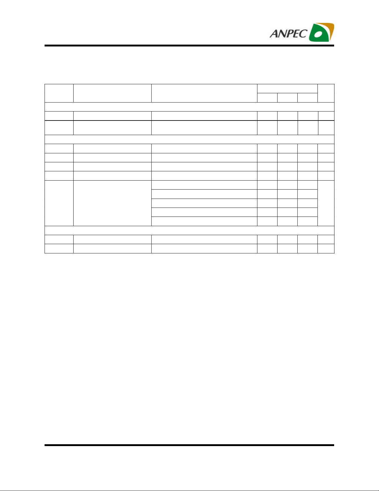
Electrical Characteristics (Cont.)
Refer to the typical application circuits. These specifications apply over V
otherwise s pecified. Typical values are at TA=25°C.
VCC=VBOOT
=5V, VIN=12V and TA= -40 ~ 85 °C, unless
Symbol
Parameter Test Conditions
APW8819
Min. Typ. Max.
PWM CONTROLLERS
FSW Operating Frequency
VIN=12V, V
VIN=12V, V
T
T
OFF(MIN)
T
ON(MIN)
Internal Soft Start Time S5 is High to V
SS
Minimum off Time
Minimum on Time 80 110 140 ns
=1.8V, R
VDDQSNS
=1.8V, R
VDDQSNS
Regulation 0.9 1.2 1.5 ms
OUT
=100 kΩ
MODE
=200 kΩ 360
MODE
270 300 330 kHz
400 440 kHz
350 450 550 ns
Zero-Crossing Threshold -9.5 0.5 10.5 mV
VDDQ PROTECTIONS
10
9
- 4500 -
0
-
125
-
-
2
3
- 16 -
2.4
2
OC Pin Source Current
OCP Comparator Offset
VDDQ Current Limit Setting Range
VDDQ OVP Trip Threshold V
VDDQ OVP Debounce Delay V
VDDQ UVP Trip Threshold V
VDDQ UVP Trip Hysteresis
VDDQ UVP Debounce
VDDQ UVP Enable Delay
TA = 25oC
Temperature Coefficient,
On The Basis of 25 οC
(VOC – V
V
– V
OC
VOC-V
VDDQ
VDDQ
VDDQ
PGND
PGND
PGND
= 60mV
) – (V
PGND
– V
Rising
Rising, DV=10mV
Falling
PHASE
),
-10
0.2
120
40 50 60
POK
V
POK Threshold
POK
I
POK Leakage Current V
POK
POK Sink Current V
POK in from Lower (POK Goes High) 87 90 93
POK Out from Normal (POK Goes Low)
=5V - 0.1 1.0
POK
=0.5V 2.5 7.5 - mA
POK
120 125 130 %
POK Enable Delay Time S5 High to POK High 2 2.4 2.8 ms
POK Delay Time Delay for POK In - 63 -
GATE DRIVERS
UGATE Pull-Up Resistance BOOT-UGATE=0.5V - 1.5 3
UGATE Sink Resistance UGATE-PHASE=0.5V - 0.7 1.8
LGATE Pull-Up Resistance VCC-LGATE=0.5V - 1 2.2
LGATE Sink Resistance LGATE-PGND=0.5V - 0.5 1.2
UGATE to LGATE Dead time UGATE falling to LGATE rising, no load - 20 - ns
LGATE to UGATE Dead time LGATE falling to UGATE rising, no load - 20 - ns
11
+10
3
130
-
-
2.8
Unit
µA
ppm/ oC
mV
V
%
µs
%
%
µs
ms
%
µA
µs
Ω
Ω
Ω
Ω
Copyright ANPEC Electro nics Corp.
www.anpec.com.tw6
Rev. A.6 - May, 2013
APW8819
Electrical Characteristics (Cont.)
Refer to the typical application circuits. These specifications apply over V
otherwise s pecified. Typical values are at TA=25°C.
VCC=VBOOT
=5V, VIN=12V and TA= -40 ~ 85 °C, unless
Symbol
Parameter Test Conditions
APW8819
Min. Typ. Max.
BOOTSTRAP SWITCH
VF RON V
IF Reverse Leakage
- V
VCC
BOOT
V
= 30V, V
BOOT
TA = 25oC
, IF = 10mA, TA = 25oC - 0.5 0.8 V
PHASE
= 25V, V
VCC
= 5V,
- - 0.5
LOGIC THRESHOLD
VIH S3, S5 High Threshold Voltage S3, S5 Rising 1.6 - - V
VIL S3, S5 Low Threshold Voltage S3, S5 Falling - - 0.9 V
I
ILEAK
I
MODE
Logic Input Leakage Current
MODE Source Current
VS3 = VS5 = 5V, TA =25oC -1 - 1
14 15 16
MODE = 0 - - 0.829
V
THMODE
MODE Threshold Voltage
MODE = 1 0.879
MODE = 2 1.262
MODE = 3 1.84
- 1.202
- 1.76
- 1.95
MODE = 4 VCC-1 - -
THERMAL SHUTDOWN
TSD Thermal Shutdown Temperature TJ Rising - 160 -
Thermal Shutdown Hysteresis - 25 -
Unit
µA
µA
µA
V
o
C
oC
Copyright ANPEC Electro nics Corp.
www.anpec.com.tw7
Rev. A.6 - May, 2013
APW8819
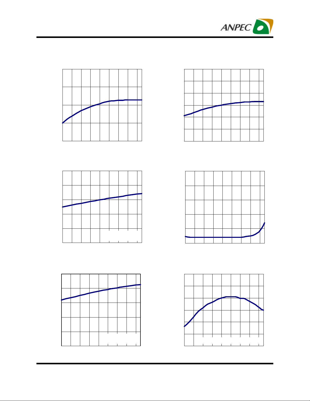
Typical Operating Characteristics
V
=1.5V, VDDQ=1.5V
REFIN
1.52
1.51
1.83
1.82
1.81
V
=1.8V, VDDQ=1.8V
REFIN
1.50
1.49
VDDQ Output Voltage (V)
1.48
-40 -20 0 20 40 60 80 100 120
Junction Temperature, TJ(oC)
Supply Current in S 0 State vs.
Junction Temperature
2.0
1.6
(mA)
VCC
1.2
0.8
0.4
Supply Current, I
S3=S5=5V
0
-40 -20 0 20 40 60 80 100 120
Junction Temperature, TJ(°C)
1.8
1.79
VDDQ Output Voltage (V)
1.78
1.77
-40 -20 0
20 40 60 80 100 120
Junction Temperature, TJ(°C)
Shutdown Current vs. Junction
Temperature
1.0
(uA)
0.8
VCC
0.6
0.4
Shutdown Current, I
0.2
0
-40 -20 0 20 40 60 80 100 120
Junction Temperature, TJ(°C)
Supply Current in S3 State vs.
Junction Temperature
1.0
0.8
(mA)
VCC
0.6
0.4
0.2
Supply Current, I
S3=0V, S5=5V
0
-40 -20 0
Copyright ANPEC Electro nics Corp.
Rev. A.6 - May, 2013
20 40 60 80 100 120
Junction Temperature, TJ (°C)
Frequency vs. Junction Temperature
330
320
SW
310
300
(KHz)
290
Switching Frequency,F
280
270
-40 -20 0 20 40 60 80 100 120
Frequency Setting : 300kHz
Junction Temperature, TJ(°C)
www.anpec.com.tw8
APW8819
Typical Operating Characteristics
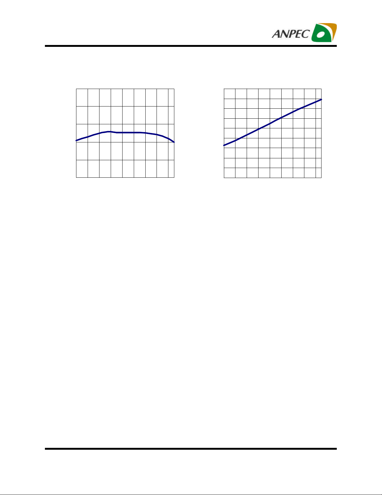
MODE Source Current vs. Junction
Temperature
20
18
16
14
12
MODE Source Current (uA)
10
-40 -20 0 20 40 60 80 100 120
Junction Temperature, TJ(°C)
OC Pin Sink Current vs. Junction
Temperature
18
16
14
12
10
8
6
OC Sink Current (uA)
4
2
0
-40 -20 0 20 40 60 80 100 120
Junction Temperature, TJ(°C)
Copyright ANPEC Electro nics Corp.
Rev. A.6 - May, 2013
www.anpec.com.tw9
 Loading...