Anpec APW8815O, APW8815QA, APW8815QB Schematics
APW8815
High-Performance Notebook PWM Controller
Features General Description
• Adjustable Output Voltage from +0.75V to +5.5V
- 0.75V Reference Voltage
- ±1% Accuracy Over-Temperature
• Operates from An Input Battery Voltage Range of
+1.8V to +28V
• Power-On-Reset Monitoring on VCC Pin and PVCC
Pin
• Excellent Line and Load Transient Responses
• PFM Mode for Increased Light Load Efficiency
• Programmable PWM Frequency from 100kHz to
500kHz
• Integrated MOSFET Drivers
• Integrated Bootstrap Forward P-CH MOSFET
• Adjustable Integrated Soft-Start and Soft-Stop
• Selectable Forced PWM or Automatic PFM/PWM
Mode
• Power Good Monitoring
• 70% Under-Voltage Protection
• 125% Over-Voltage Protection
• Adjustable Current-Limit Protection
- Using Sense Low-Side MOSFET’s R
DS(ON)
• Over-Temperature Protection
• TSSOP-14, QFN3.5x3.5-14, and TQFN3x3-16
Packages
• Lead Free and Green Devices Available
(RoHS Compliant)
The APW8815 is a single-phase, constant-on-time,
synchronous PWM controller, which drives N-channel
MOSFETs. The APW8815 steps down high voltage to
generate low-voltage chipset or RAM supplies in notebook
computers.
The APW8815 provides excellent transient response and
accurate DC voltage output in either PFM or PWM Mode.
In Pulse Frequency Mode (PFM), the APW8815 provides
very high efficiency over light to heavy loads with loadingmodulated switching frequencies. In PWM Mode, the
converter works nearly at constant frequency for low-noise
requirements.
The APW8815 is equipped with accurate positive currentlimit, output under-voltage, and output over-voltage
protections, perfect for NB applications. The Power-OnReset function monitors the voltage on VCC and PVCC to
prevent wrong operation during power-on. The APW8815
has a 1.2ms digital soft-start and built-in an integrated
output discharge device for soft-stop. An internal
integrated soft-start ramps up the output voltage with
programmable slew rate to reduce the start-up current. A
soft-stop function actively discharges the output
capacitors.
The APW8815 is available in 14pin TSSOP, 14pin QFN
and 16pin TQFN packages respectively.
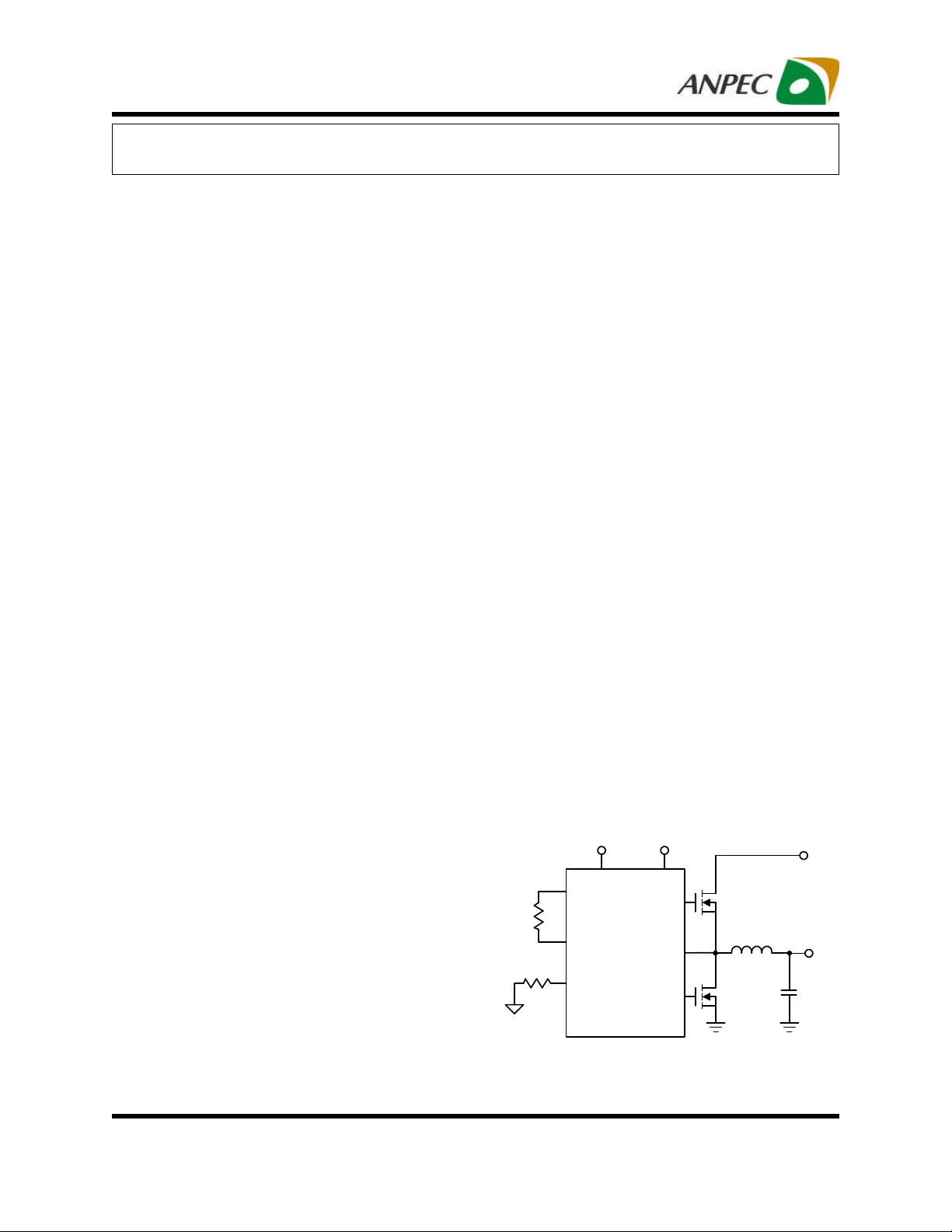
Simplified Application Circuit
VCC=5V
EN
V
IN
Applications
• Notebook
• Table PC
• Hand-Held Portable
• AIO PC
R
TON
R
OCSET
PHASE
TON
OCSET
UGATE
PHASE
LGATE
Q2
Q1
L
V
OUT
APW8815
ANPEC reserves the right to make changes to improve reliability or manufacturability without notice, and
advise customers to obtain the latest version of relevant information to verify before placing orders.
Copyright ANPEC Electronics Corp.
Rev. A.2 - Apr., 2011
www.anpec.com.tw1
APW8815
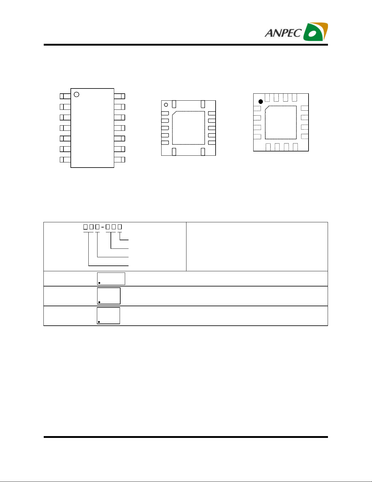
Pin Configuration
EN
1
TON
2
VOUT
VCC
FB
POK
3
4
5
6
7
TSSOP-14
(Top View)
14
13
12
11
10
9
8
BOOT
UGATE
PHASE
OCSET
PVCC
LGATE
PGNDGND
TON
VOUT
VCC
FB
POK
EN
1
2
3
4
5
6
7
GND
QFN3.5x3.5-14
(Top View)
EN
TON
NC
BOOT
BOOT
14
UGATE
13
PHASE
12
OCSET
11
PVCC
10
LGATE
9
8
PGND
V
OUT
C
V
F
O
P
C
B
K
16
15
1
2
3
4
5
NC
13
14
12
11
10
8
7
6
GND
PGND
LGATE
T
E
G
A
U
E
PHA
S
CSE
T
O
C
C
P
V
9
TQFN3x3-16
(Top View)
Ordering and Marking Information
APW8815
Assembly Material
Handling Code
Temperature Range
Package Code
APW8815 O :
APW8815 QA : XXXXX - Date Code
APW8815 QB : XXXXX - Date Code
Note: ANPEC lead-free products contain molding compounds/die attach materials and 100% matte tin plate termination finish; which
are fully compliant with RoHS. ANPEC lead-free products meet or exceed the lead-free requirements of IPC/JEDEC J-STD-020D for
MSL classification at lead-free peak reflow temperature. ANPEC defines “Green” to mean lead-free (RoHS compliant) and halogen
free (Br or Cl does not exceed 900ppm by weight in homogeneous material and total of Br and Cl does not exceed 1500ppm by
weight).
APW8815
XXXXX
APW
8815
XXXXX
APW
8815
XXXXX
Package Code
O : TSSOP-14 QA : QFN3.5x3.5-14 QB : TQFN3x3-16
Temperature Range
I : -40 to 85 oC
Handling Code
TR : Tape & Reel
Assembly Material
G : Halogen and Lead Free Device
XXXXX - Date Code
Copyright ANPEC Electro nics Corp.
Rev. A.2 - Apr., 2011
www.anpec.com.tw2
APW8815
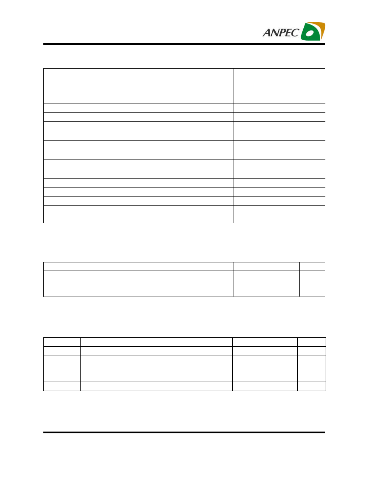
Absolute Maximum Ratings (Note 1)
Symbol Parameter Rating Unit
VCC VCC Supply Voltage (VCC to GND) -0.3 ~ 7 V
V
PVCC Supply Voltage (PVCC to GND) -0.3 ~ 7 V
PVCC
V
Note 1: Absolute Maximum Ratings are those values beyond which the life of a device may be impaired. Exposure to absolute
maximum rating conditions for extended periods may affect device reliability.
BOOT Supply Voltage (BOOT to GND or PGND) -0.3 ~ 35 V
BOOT-GND
V
BOOT Supply Voltage (BOOT to PHASE) -0.3 ~ 7 V
BOOT
All Other Pins (VOUT, OCSET, TON, EN and FB to GND) -0.3 ~ VCC+0.3 V
<400ns Pulse Width
>400ns Pulse Width
LGATE Voltage (LGATE to GND)
UGATE Voltage (UGATE to PHASE)
<400ns Pulse Width
>400ns Pulse Width
PHASE Voltage (PHASE to GND)
V
PHASE
<400ns Pulse Width
>400ns Pulse Width
V
POK Supply Voltage (POK to GND) -0.3 ~ 7 V
POK
V
PGND to GND Voltage -0.3 ~ 0.3 V
PGND
-5 ~ V
-0.3 ~ V
BOOT
BOOT
+0.3
-5 ~ VCC+0.3
-0.3 ~ VCC+0.3
-5 ~ 35
-1 ~ 28
+0.3
TJ Maximum Junction Temperature 150
T
Storage Temperature -65 ~ 150
STG
T
Maximum Soldering Temperature, 10 Seconds 260
SDR
V
V
V
o
C
o
C
o
C
Thermal Characteristics
Symbol Parameter Typical Value Unit
Thermal Resistance-Junction to Ambient
θJA
Note 2: θJA are measured with the component mounted on a high effective the thermal conductivity test board in free air. The exposed
(Note2)
QFN3.5x3.5-14
TQFN3x3-16
TSSOP-14
100
80
40
°C/W
pad of package is soldered directly on the PCB.
Recommended Operating Conditions (Note 3)
Symbol Parameter Range Unit
VIN
VCC, PVCC VCC, PVCC Supply Voltage 4.5 ~ 5.5 V
V
OUT
TA
TJ
Note 3: Refer to the typical application circuit.
Converter Input Voltage 1.8 ~ 28 V
Converter Output Voltage 0.75 ~ 5.5 V
Ambient Temperature -40 ~ 85
Junction Temperature -40 ~ 125
o
C
o
C
Copyright ANPEC Electro nics Corp.
Rev. A.2 - Apr., 2011
www.anpec.com.tw3
APW8815
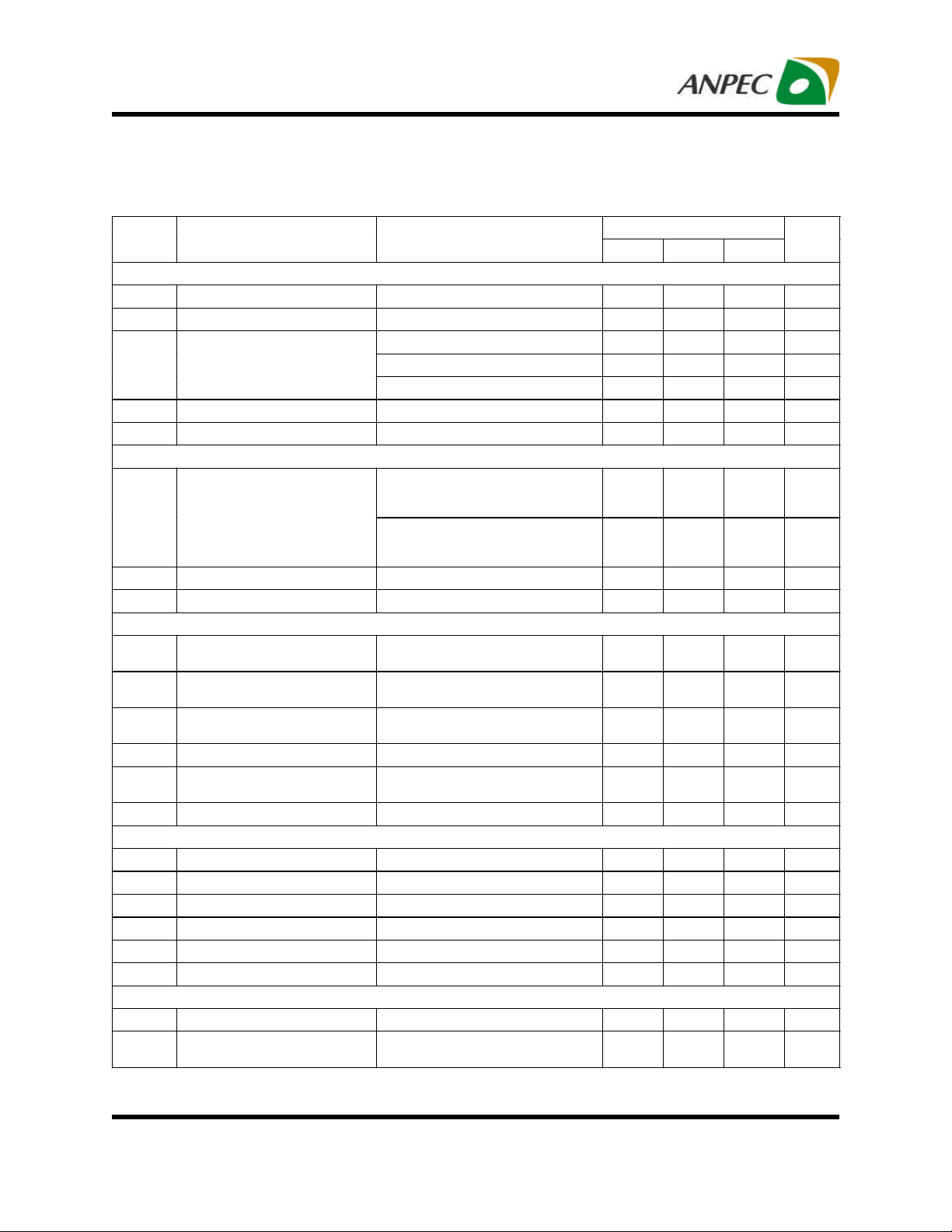
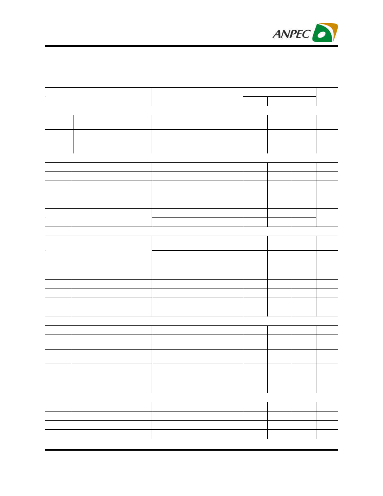
Electrical Characteristics
These specifications apply for TA=-40°C to +85°C, unless otherwise stated. All typical specifications TA=+25°C, VCC=5V,
V
=5V.
PVCC
Symbol
Parameter Test Conditions
VOUT AND VFB VOLTAGE
V
Output Voltage Adjustable output range 0.75 - 5.5 V
OUT
V
Reference Voltage - 0.75 - V
REF
TA = 25 oC -0.5 - +0.5 %
Regulation Accuracy
TA = 0 oC ~ 85 oC -0.8 - +0.8 %
TA = -40 oC ~ 85 oC -1.0 - +1.0 %
IFB FB Input Bias Current FB = 0.75V - 0.02 0.1
R
VOUT Discharge Resistance EN = 0V, V
DIS
= 0.5V - 20 50
OUT
SUPPLY CURRENT
VCC Plus PVCC Current, PWM,
EN = Float, VFB = 0.77V,
I
VCC Input Bias Current
VCC
PHASE = -0.1V
VCC Plus PVCC Current, PFM,
EN = 5V, VFB = 0.77V,
PHASE = 0.5V
I
VCC_SHDN
I
VCC_SHDN
VCC Shutdown Current EN = GND, VCC = 5V - 4.5 7.5
PVCC Shutdown Current EN = GND, PVCC = 5V - 0 1.0
ON-TIME TIMER AND INTERNAL SOFT-START
V
= 12V, V
T
Nominal On Time
ONN
T
Fast On Time
ONF
T
Slow On Time
ONS
T
ON(MIN)
T
OFF(MIN)
Minimum On Time 80 110 140 ns
Minimum Off Time
PHASE
R
= 250kΩ
TON
V
= 12V, V
PHASE
R
= 100kΩ
TON
V
= 12V, V
PHASE
R
= 400kΩ
TON
VFB = 0.7V, V
OCSET = OPEN
TSS Internal Soft-Start Time EN High to V
= 2.5V,
OUT
= 2.5V,
OUT
= 2.5V,
OUT
= -0.1V,
PHASE
Regulation 0.9 1.2 1.5 ms
OUT
GATE DRIVER
UG Pull-Up Resistance BOOT-UG = 0.5V - 5 7
UG Sink Resistance UG-PHASE = 0.5V - 1 2.5
LG Pull-Up Resistance PVCC-LG = 0.5V - 5 7
LG Sink Resistance LG-PGND = 0.5V - 0.9 2.5
UG to LG Dead Time UG falling to LG rising, no load - 40 - ns
LG to UG Dead Time LG falling to UG rising, no load - 40 - ns
BOOTSTRAP SWITCH
VF Ron V
IR Reverse Leakage
PVCC
V
BOOT-GND
V
PVCC
- V
BOOT-GND
= 30V, V
= 5V
, IF = 10mA - 0.5 0.8 V
= 25V,
PHASE
Min.
APW8815
Typ. Max.
Unit
µA
- 400 750
- 250 470
µA
µA
µA
µA
- 749 - ns
280 330 380 ns
- 1170 - ns
350 450 550 ns
- - 0.5
µA
Ω
Ω
Ω
Ω
Ω
Copyright ANPEC Electro nics Corp.
www.anpec.com.tw4
Rev. A.2 - Apr., 2011
APW8815
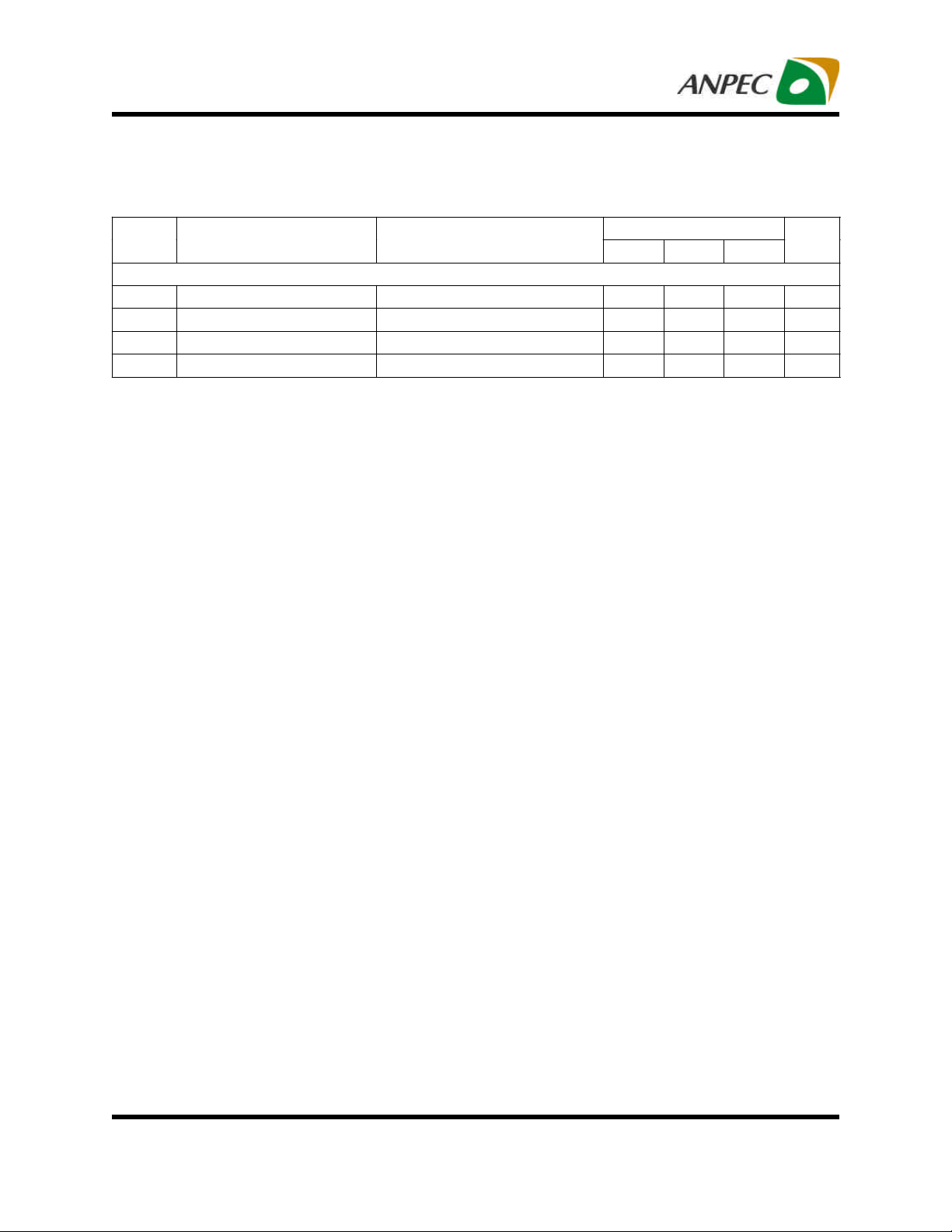
Electrical Characteristics (Cont.)
These specifications apply for TA=-40°C to +85°C, unless otherwise stated. All typical specifications TA=+25°C, VCC=5V,
V
=5V.
PVCC
Symbol
Parameter Test Conditions
VCC POR THRESHOLD
V
PVCC_THR
V
VCC_THR
Rising PVCC POR Threshold
Voltage
Rising VCC POR Threshold
Voltage
4.2 4.35 4.45 V
4.2 4.35 4.45 V
VCC POR Hysteresis - 100 - mV
CONTROL INPUTS
EN High Threshold 2.5 2.65 2.8 V
Hysterisis 100 175 225 mV
EN Float Threshold 1.37 1.95 2.39 V
EN Low Threshold 0.7 1.0 1.3 V
Hysterisis 150 200 250 mV
EN Leakage
EN = 0V - 0.1 1.0
EN = 5V - - 2.0
POWER-OK INDICATOR
POK in from Lower (POK Goes
High)
V
POK Threshold
POK
POK Low Hysteresis (POK Goes
Low)
POK out from Normal (POK Goes
Low)
I
POK Leakage Current V
POK
POK Sink Current V
= 5V - 0.1 1.0
POK
= 0.5V 2.5 7.5 - mA
POK
POK Debounce Time 43 63 85
POK Enable Delay Time EN High to POK High 1.4 2.0 2.6 ms
CURRENT SENSE
I
OCSET
T
CIOCSET
V
ROCSET
I
OCP Threshold I
OCSET
I
Temperature
OCSET
Coefficient
Current-Limit Threshold
Setting Range
Over Current-Limit
Comparator Offset
Zero Crossing Comparator
Offset
Sourcing 9 10 11
OCSET
On The Basis of 25°C - 4500 V
OCSET-GND
Voltage, Over All
Temperature
(V
OCSET-GND-VPGND-PHASE
V
OCSET-GND
V
PGND-PHASE
= 60mV
Voltage, EN = 3.3V -9.5 0.5 10.5 mV
) Voltage,
PROTECTION
VUV UVP Threshold 60 70 80 %
UVP Hysteresis - 3 - %
UVP Debounce Interval - 16 UVP Enable Delay EN High to UVP Workable 1.4 2 2.6 ms
APW8815
Min. Typ. Max.
Unit
µA
87 90 93 %
- 3 - %
120 125 130 %
µA
µs
µA
ppm/
o
30 - 200 mV
-10 0 10 mV
µs
C
Copyright ANPEC Electro nics Corp.
www.anpec.com.tw5
Rev. A.2 - Apr., 2011
APW8815
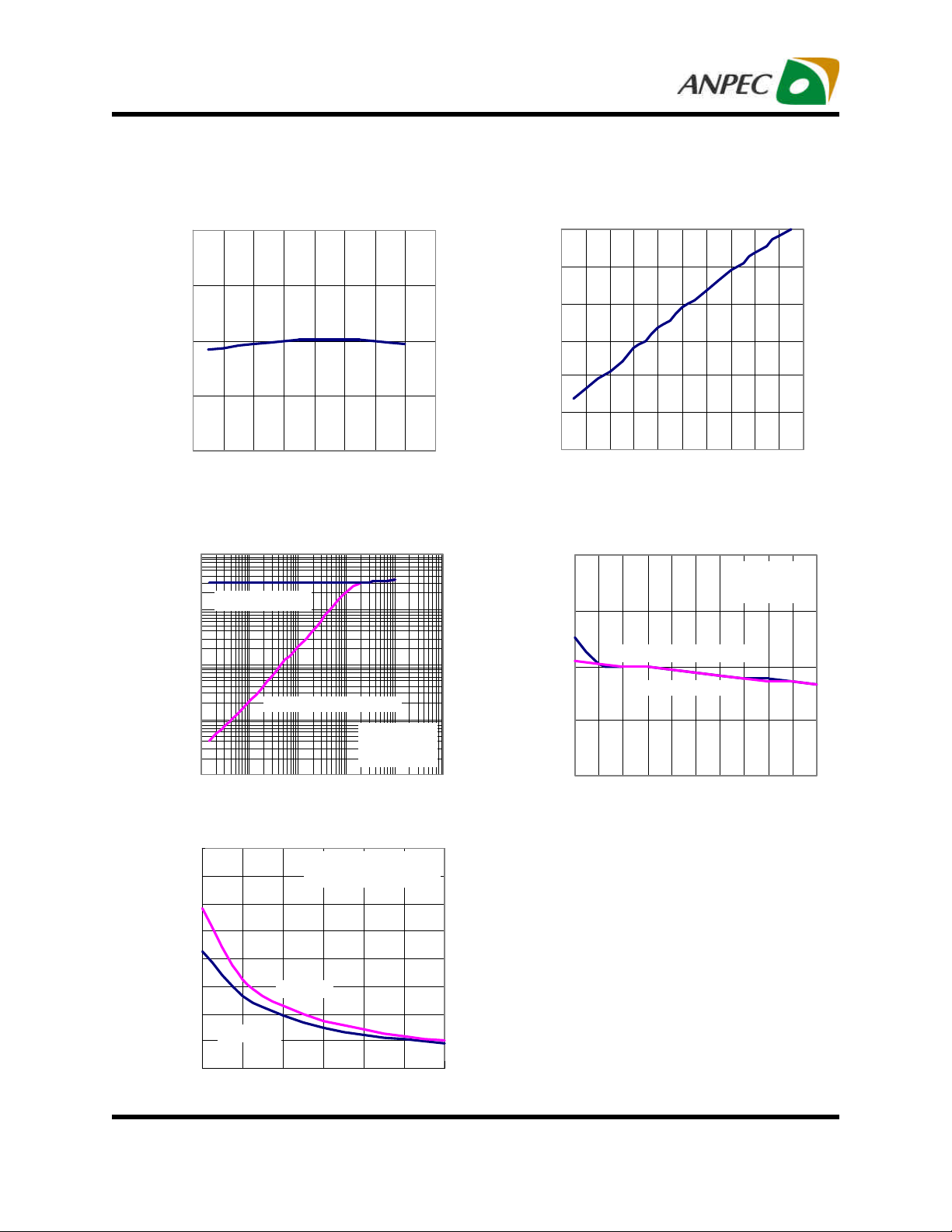
Electrical Characteristics (Cont.)
These specifications apply for TA=-40°C to +85°C, unless otherwise stated. All typical specifications TA=+25°C, VCC=5V,
V
=5V.
PVCC
Symbol
Parameter Test Conditions
PROTECTION (CONT.)
V
OVP Rising Threshold 120 125 130 %
OVR
OVP Propagation Delay VFB Rising, DV = 10mV - 1.5 -
T
OTP Rising Threshold
OTR
OTP Hysteresis
Note 4: Guaranteed by design.
(Note 4)
- 160 -
(Note 4)
- 25 -
Min.
APW8815
Typ. Max.
Unit
µs
o
C
o
C
Copyright ANPEC Electro nics Corp.
www.anpec.com.tw6
Rev. A.2 - Apr., 2011
APW8815
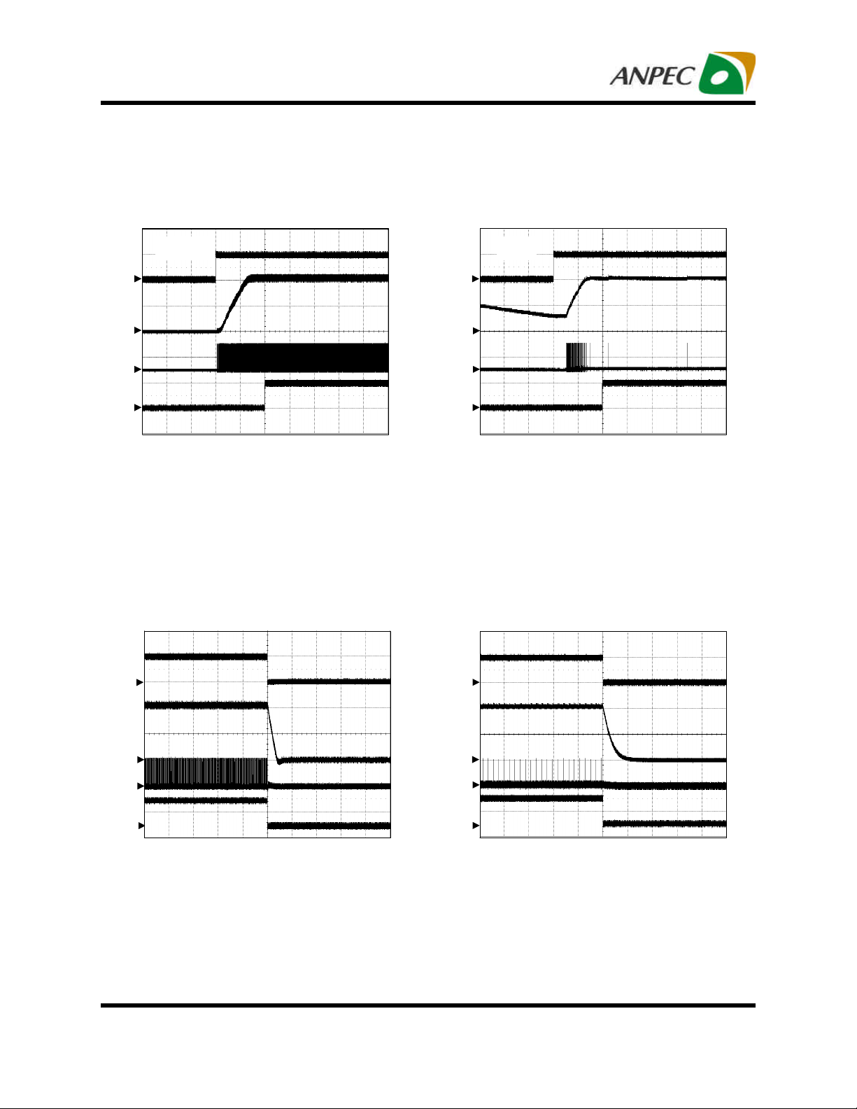
Typical Operating Characteristics
0.760
(V)
REF
0.755
0.750
0.745
Reference Voltage Accuracy, V
0.740
(kHz)
SW
Reference Voltage Accuracy vs.
Junction Temperature
-50 -30 10 50 90 1107030-10
Junction Temperature, TJ (oC)
Switching Frequency vs.
Converter Output Current
1000
Forced-PWM Mode
100
OCSET Sourcing Current vs.
Junction Temperature
16
(µA)
14
OCSET
12
10
8
6
OCSET Sourcing Current, I
4
-50 -30 10 50 90 110 1507030-10 130
Junction Temperature, TJ (oC)
Converter Output Voltage vs.
Converter Output Current
1.070
(V)
OUT
1.060
VIN=19V,
V
=1.05V,
OUT
FSW=200kHz
10
Automatic PFM/PWM Mode
1
Switching Frequency, F
0.1
0.001 0.01 0.1
1
Converter Output Current, I
Switching Frequency vs. TON Resistance
800
700
(kHz)
600
SW
500
400
300
200
Switching Frequency, F
100
0
100
V
OUT
↑
=1.05V
TON Resistance, R
Copyright ANPEC Electro nics Corp.
Rev. A.2 - Apr., 2011
VIN=19V, Forced-PWM Mode
V
=2.5V
OUT
↓
VIN=19V,
V
=1.05V,
OUT
FSW=300kHz
10
OUT
(kΩ)
TON
(A)
100
700600500400300200
Converter Output Voltage, V
1.050
1.040
1.030
Automatic PFM/PWM Mode
Forced-PWM Mode
0
Converter Output Current, I
987654321 10
(A)
OUT
www.anpec.com.tw7
APW8815
Operating Waveforms
Refer to the typical application circuit. The test condition is VIN=19V, TA=25oC unless otherwise specified.
Enable at Zero Initial Voltage of V
I
=5A
LOAD
1
2
3
4
CH1: VEN, 5V/Div, DC
CH2: V
CH3: V
CH4: V
TIME: 1ms/Div
, 500mV/Div, DC
OUT
, 20V/Div, DC
PHASE
, 5V/Div, DC
POK
Shutdown at I
OUT
=5A
OUT
Enable Before End of Soft-Stop
No Load
1
2
3
4
CH1: VEN, 5V/Div, DC
CH2: V
CH3: V
CH4: V
TIME: 1ms/Div
, 500mV/Div, DC
OUT
, 20V/Div, DC
PHASE
, 5V/Div, DC
POK
Shutdown with Soft-Stop at No Load
1
2
3
4
CH1: VEN, 5V/Div, DC
CH2: V
CH3: V
CH4: V
TIME: 20µs/Div
, 500mV/Div, DC
OUT
, 20V/Div, DC
PHASE
, 5V/Div, DC
POK
Copyright ANPEC Electro nics Corp.
Rev. A.2 - Apr., 2011
1
2
3
4
CH1: VEN, 5V/Div, DC
CH2: V
CH3: V
CH4: V
TIME: 20ms/Div
, 500mV/Div, DC
OUT
, 20V/Div, DC
PHASE
, 5V/Div, DC
POK
www.anpec.com.tw8
APW8815
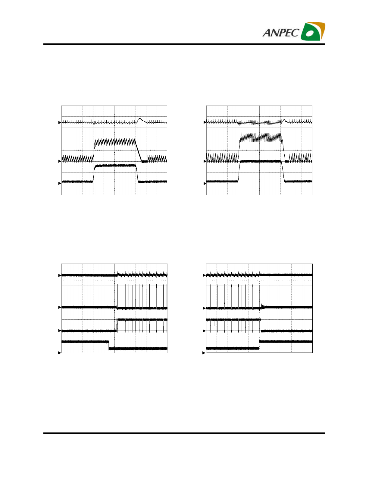
Operating Waveforms (Cont.)
Refer to the typical application circuit. The test condition is VIN=19V, TA=25oC unless otherwise specified.
Load Transient
V
=1.05V, 1A->8A->1A
OUT
1
2
3
CH1: V
, 100mV/Div, AC
OUT
CH2: IL, 5A/Div, DC
CH3: I
, 5A/Div, DC
OUT
TIME: 20µs/Div
Mode Transient From PFM to PWM
Load Transient
V
=2.5V, 1A->10A->1A
OUT
1
2
3
CH1: V
, 100mV/Div, AC
OUT
CH2: IL, 5A/Div, DC
CH3: I
, 5A/Div, DC
OUT
TIME: 20µs/Div
Mode Transient From PWM to PFM
1
2
3
4
CH1: V
CH2: V
CH3: V
, 100mV/Div, AC
OUT
, 10V/Div, DC
PHASE
, 5V/Div, DC
LGATE
CH4: VEN, 5V/Div, DC
TIME: 10µs/Div
Copyright ANPEC Electro nics Corp.
Rev. A.2 - Apr., 2011
1
2
3
4
CH1: V
CH2: V
CH3: V
, 100mV/Div, AC
OUT
, 10V/Div, DC
PHASE
, 5V/Div, DC
LGATE
CH4: VEN, 5V/Div, DC
TIME: 10µs/Div
www.anpec.com.tw9
 Loading...