APW8807
8A Synchronous Buck Converter
Features General Description
• Wide Input voltage Range from 6V to 28V
• Provide PWM Converter with Adjustable 0.6V to 5.
5V Output
- 0.6V Reference Voltage
- Excellent Line/Load Regulations about +1.5%
over temperature range at PWM Channel
• Built in POR Control Scheme Implemented
• 15mA 5V Voltage Output
• Constant On-Time Control Scheme with Frequency
Compensation for PWM Mode
• Built in Soft Start for PWM Output and Soft Stop
for PWM Output and LDO Output
• Integrated Bootstrap Forward P-CH MOSFET
• High Efficiency over Light to Full Load Range
(PWMs)
• Built in Power Good Indicators (PWM)
• Integrated 24mΩ at VCC=5V N-Channel MOSFET
For High Side
• Integrated 14mΩ at VCC=5V N-Channel MOSFET
For Low Side
• 60% Under-Voltage and 120% Over-Voltage
Protections (PWM)
• Fixed Current-Limit Protection at 11A Loading
(PWM)
• Over-Temperature Protection
• 3mmx3mm Thin QFN-16A (TQFN3x3-16A) package
• Lead Free and Green Device Available (RoHS
Compliant)
The APW8807 integrates the step-down, constant
on-time, synchronous PWM converter with 24Ω Nchannel high side MOSFET and 14Ω N-channel low side
MOSFET, as well as various protections into a chip. The
PWM converter step down high voltage of a battery to
generate low-voltage, for NB applications.
The APW8807 provides excellent transient response and
accurate DC output voltage in automatic PFM/PWM Mode.
In Pulse-Frequency Mode (PFM), the APW8807 provides
very high efficiency over light to heavy loads with loadingmodulated switching frequencies. The PWM mode works
nearly at constant frequency for low-noise requirements.
The APW8807 is equipped with accurate sourcing
current-limit, output under-voltage, output over-voltage
protections, being perfect for NB applications. A 4.8ms
(Typ.) soft-start can reduce the start-up current. A softstop function actively discharges the output capacitors by
the discharge switch.
The APW8807 has enable control for PWM. Pulling the
EN pin low shuts down the PWM output. The APW8807 is
available in a TQFN3x3-16A package.
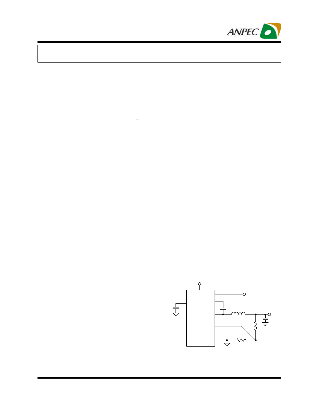
Simplified Application Circuit
EN
V
IN
BOOT
VCC
L
OUT
LX
POK
FB
V
OUT
AGND
APW8807
ANPEC reserves the right to make changes to improve reliability or manufacturability without notice, and
advise customers to obtain the latest version of relevant information to verify before placing orders.
Copyright ANPEC Electronics Corp.
Rev. A.1 - Nov., 2013
www.anpec.com.tw1
APW8807
Applications
• Notebook and Sub-Notebook Computers
• Portable Devices
• DDR1, DDR2, and DDR3 Power Supplies
• 3-Cell and 4-Cell Li+ Battery-Powered Devices
• Graphic Cards
• Game Consoles
• Telecommunications
Ordering and Marking Information
APW8807
APW8807 QB:
Assembly Material
Handling Code
Temperature Range
Package Code
APW
8807
XXXXX
Package Code
QB : TQFN3x3-16A
Operating Junction Temperature
I : -40 to 85oC
Handling Code
TR : Tape & Reel
Assembly Material
G : Halogen and Lead Free Device
X - Date Code
Note: ANPEC lead-free products contain molding compounds/die attach materials and 100% matte tin plate termination finish; which
are fully compliant with RoHS. ANPEC lead-free products meet or exceed the lead-free requirements of IPC/JEDEC J-STD-020D for
MSL classification at lead-free peak reflow temperature. ANPEC defines “Green” to mean lead-free (RoHS compliant) and halogen
free (Br or Cl does not exceed 900ppm by weight in homogeneous material and total of Br and Cl does not exceed 1500ppm by
weight).
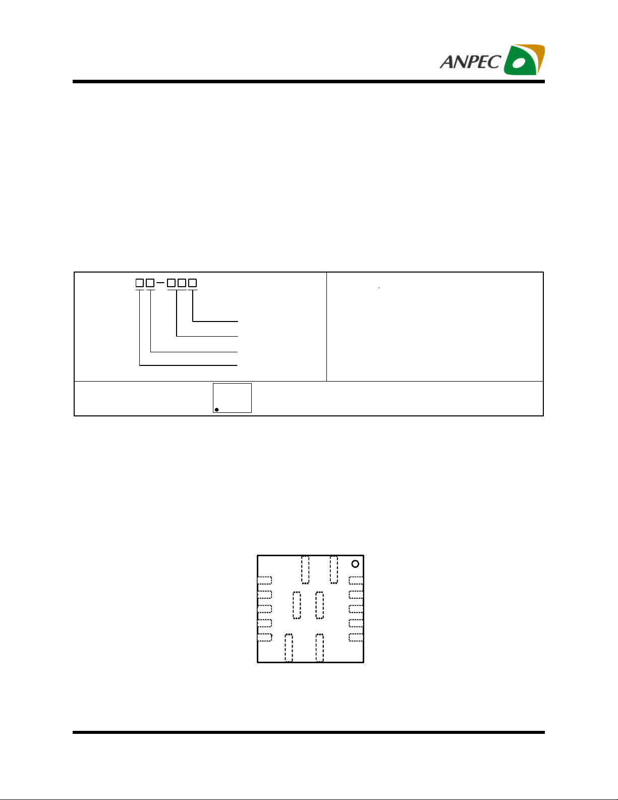
Pin Configuration
PGND
VIN
2
1
AGND
14
15 LX
9
LX
13
12
11
10
EN
FB
VCC
BOOT
NC
POK
NC
NC
VOUT
3
4
5
6
7
16 LX
8
LX
Copyright ANPEC Electronics Corp.
Rev. A.1 - Nov., 2013
TQFN 3 x 3 -16A
Top View
www.anpec.com.tw2
APW8807
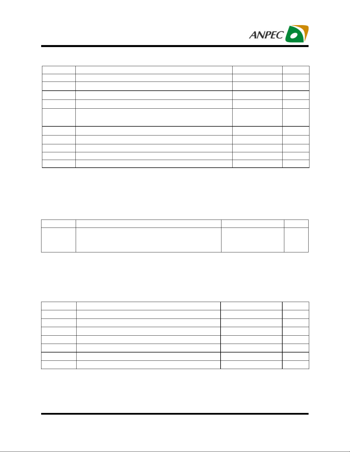
Absolute Maximum R atings (Note 1)
Symbol Parameter Rating Unit
VCC
VIN Input Power Voltage (VIN to GND) -0.3 ~ 30 V
V
BOOT
V
BOOT-GND
VLX
V
GND
TJ Maximum Junction Temperature 150
T
STG
T
SDR
Note1: Stresses beyond those listed under "absolute maximum ratings" may cause permanent damage to the device. These are
stress ratings only and functional operation of the device at these or any other conditions beyond those indicated under "recommended operating conditions" is not implied. Exposure to absolute maximum rating conditions for extended periods may affect device
reliability.
VCC Supply Voltage (VCC to GND) -0.3 ~ 7 V
BOOT Supply Voltage (BOOT to LX) -0.3 ~ 7 V
BOOT Supply Voltage (BOOT to GND) -0.3 ~ 37 V
LX Voltage (LX to GND)
<20ns pulse width
>20ns pulse width
-5 ~ 37
-0.3 ~ 30
All Other Pins (LDO, VCLK, ENLDO, EN, VOUT, POK to GND) -0.3 ~ VCC+0.3 V
AGND to PGND -0.3 ~ +0.3 V
Storage Temperature -65 ~ 150
Maximum Lead Soldering Temperature(10 Seconds) 260
V
o
C
o
C
o
C
Thermal Characteristics
Symbol Parameter Typical Value Unit
θJA
Note 2: θJA is measured with the component mounted on a high effective thermal conductivity test board in free air.
Junction-to-Ambient Resistance in free air
(Note 2)
TQFN3x3-16A
95
Recommended Operating Conditions (Note 3)
Symbol Parameter Range Unit
VIN
VCC VCC Supply Voltage 4.5 ~ 5.5 V
V
OUT_PWM
I
OUT_PWM
CIN PWM Converter Input Capacitor (MLCC) 10 ~
TA
TJ
Note 3: Refer to the typical application circuit.
PWM Converter Input Voltage 6 ~ 28 V
PWM Converter Output Voltage 0.6 ~ 5.5 V
PWM Converter Output Current 0~8 A
Ambient Temperature
Junction Temperature
-40 ~ 85
-40 ~ 125
°C/W
µF
o
C
o
C
Copyright ANPEC Electronics Corp.
Rev. A.1 - Nov., 2013
www.anpec.com.tw3
APW8807
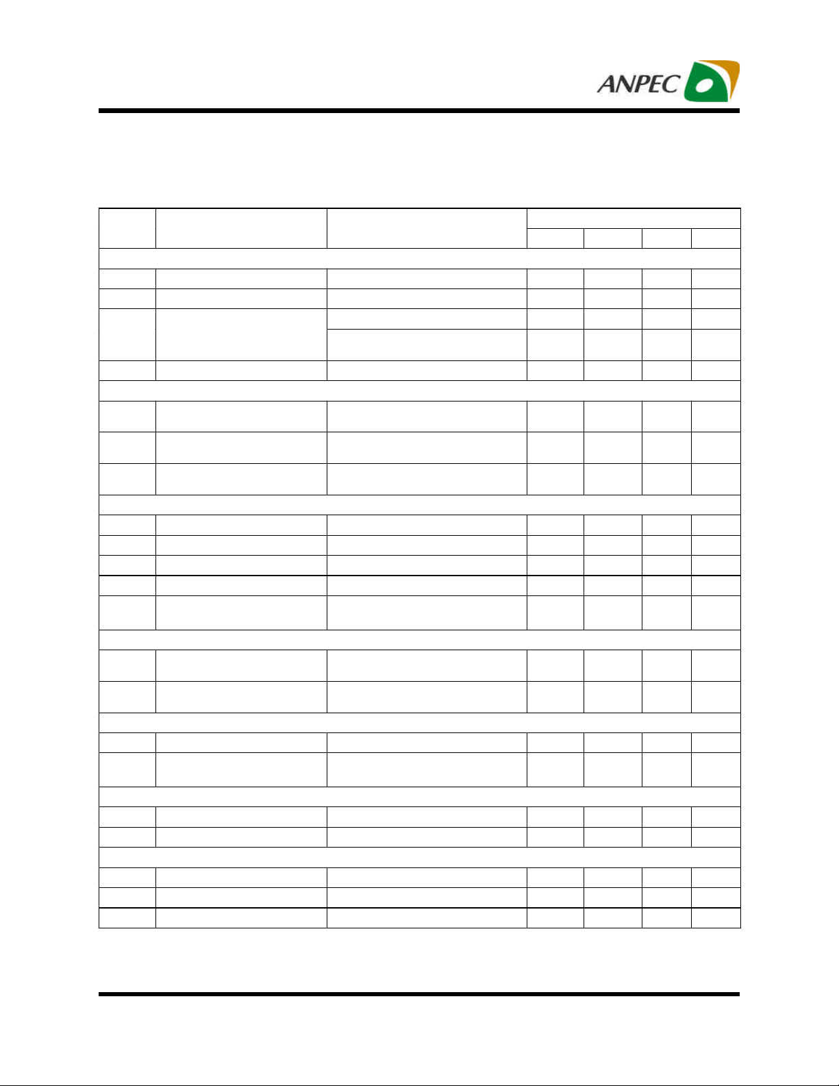
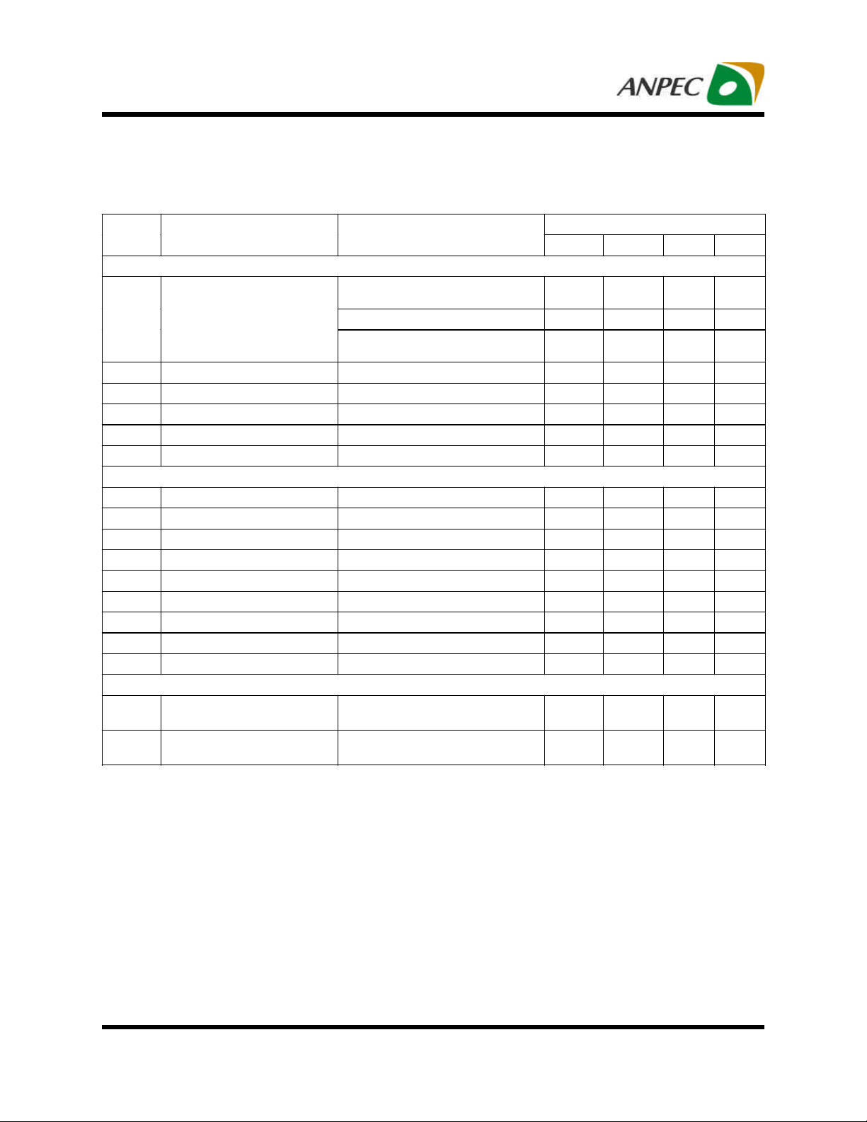
Electrical Characteristics
Unless otherwise specified, these specifications apply over VCC=5V, VIN=12V and TA= -40 to 85 oC. Typical values are
at TA=25oC.
Symbol
Parameter Test Condition
Min.
APW8807
Typ. Max. Unit
VOUT PIN AND VOUT VOLTAGE
V
Output Voltage Setting Range 0.6 -
OUT
5.5 V
REF voltage - 0.6 -
TA = 25 oC -0.5 - +0.5 %
Regulation Accuracy
R
VOUT Discharge Resistance EN=0V, V
DIS
TA = -40 oC ~ 85 oC, Line & Load
Regulations
=0.5V - 80
OUT
-1.5 - +1.5 %
SUPPLY CURRENT
I
VIN_PWM
I
VIN_PFM
I
VIN_SD
VIN Supply Current at PWM
Mode
VIN Supply Current at PFM
Mode
VIN Supply Current at
Shutdown Mode
VOUT=5.5V, EN=5V, I
VOUT=5.5V, EN=5V, I
=3A 1.53 A
OUT
=0A - 80 100
OUT
EN=0V - - 10
ON-TIME TIMER AND INTERNAL SOFT START AND ZERO CROSSING
FSW Switching Frequency at PWM VIN=12V, V
T
ON(MIN)
T
OFF(MIN)
- 100 - ns
Minimum off time VFB=0.55V, V
TSS Internal Soft Start Time EN High to V
VZC
Zero Crossing Comparator
Offset
V
GND-VLX
=5.05V 450 500 550 kHz
OUT
=-0.1V 200 300 400 ns
PHASE
Regulation 95% - 4.8 - ms
OUT
-5 - 5 mV
INTERNAL POWER MOSFETS AND DEAD TIME
R
DS(ON)_H
R
DS(ON)_L
High Side N-MOSFET
Resistance
Low Side N-MOSFET
Resistance
VCC=5V - 24 30
VCC=5V - 14 18
BOOTSTRAP SWITCH
VF Ron V
IR Reverse Leakage
VCC
V
BOOT-GND
V
VCC
– V
, IF = 10mA - 0.15 0.25 V
BOOT-GND
= 30V, VLX = 25V,
= 5V
- - 0.5
VCC POR THRESHOLD
V
POR_VCC
VCC POR Threshold Voltage 4.25 4.35 4.45 V
VCC POR Hysteresis - 100 - mV
CONTROL INPUTS
EN Leakage EN=0V - 0.1 1.0
EN Low Threshold EN falling 1.05 1.35 1.65 V
Hys. - 200 - mV
Ω
µA
µA
Ω
Ω
µA
µA
Copyright ANPEC Electronics Corp.
Rev. A.1 - Nov., 2013
www.anpec.com.tw4
APW8807
Electrical Characteristics(Cont.)
Unless otherwise specified, these specifications apply over VCC=5V, VIN=12V and TA= -40 to 85 oC. Typical values are
at TA=25oC.
Symbol
Parameter Test Condition
Min.
APW8807
Typ. Max. Unit
POWER-OK INDICATOR
V
POK Threshold
POK
I
POK Leakage Current V
POK
POK Sink Current V
POK in from Lower (POK Goes
High)
POK Low Hystersis - 3 - %
POK out from Normal high
threshold (POK Goes Low)
=5V - 0.1 1.0
POK
=0.5V 2 4 - mA
POK
87 90 93 %
115 120 125 %
POK Out Debounce Time1 When enter 120% threshold - 2 POK Out Debounce Time2 When enter 87% threshold - 16 POK Enable Delay Time From EN High to POK High - 5.3 - ms
PROTECTION
ICL Low Side Current Limit Valley current 10 11 12 A
VUV UVP Threshold 55 60 65 %
UVP Debounce Interval - 2 UVP Enable Delay EN high to UVP workable - 5.3 - ms
V
OVP Rising Threshold 115 120 125 %
OVP
HYS - 10 - %
OVP Propagation Delay VFB Rising, Over voltagee=10mV - 2 -
T
OTP Rising Threshold
OTP
OTP Hysteresis
(Note 5)
- 150 -
(Note 5)
- 40 -
VCC Regulator
µA
µs
µs
µs
µs
o
C
o
C
VCC Regulator Output Voltage
VCC Load Regulation
VIN=6V~28V, no load
Icc=15mA
4.8 5 5.2
- 5 -
V
%
Copyright ANPEC Electronics Corp.
www.anpec.com.tw5
Rev. A.1 - Nov., 2013
APW8807
serves as the lower supply rail for the
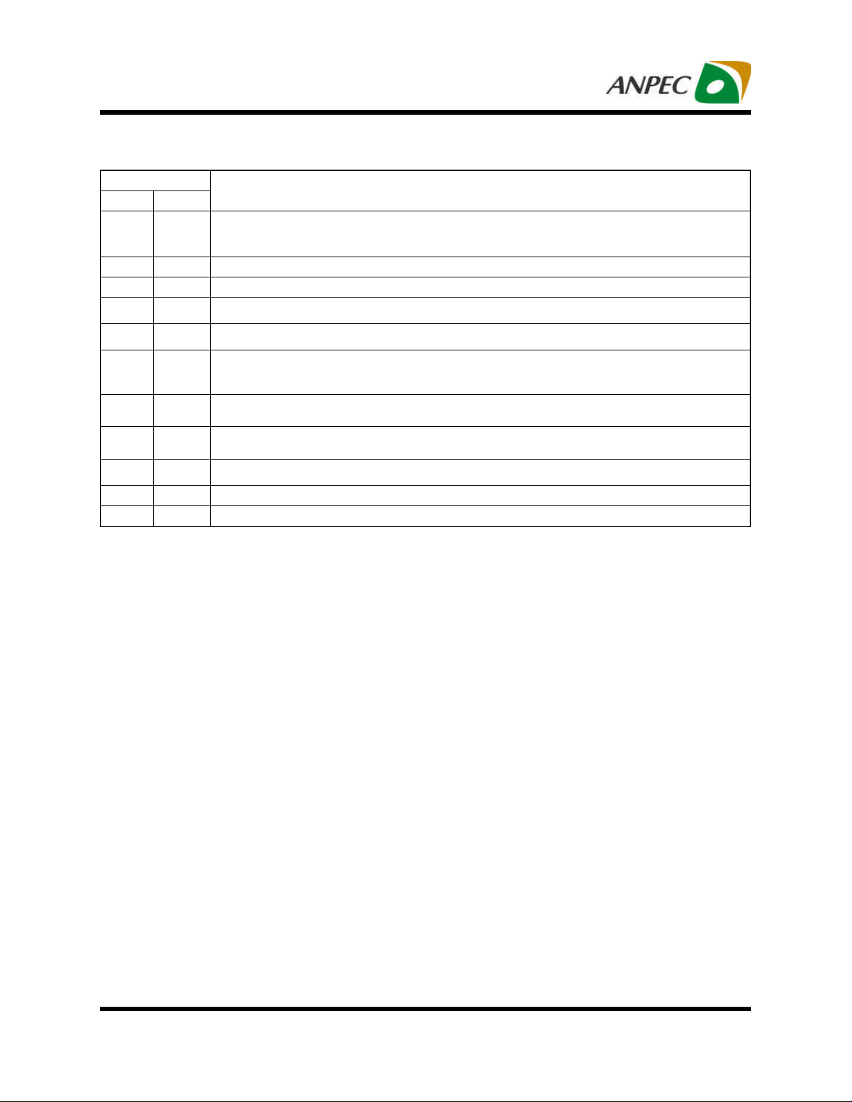
Pin Description
PIN
NO. NAME
1 VIN
2
3, 5, 6
4 POK
7 VOUT
8,
9,15,16
10 BOOT
11 VCC
12 FB
13 EN PWM Enable. PWM is enabled when EN=1. When EN=0, PWM is in shutdown.
14 AGND Signal Ground for The IC.
PGND Power Ground of The LGATE Low-Side MOSFET Drivers.
NC No Connection
Battery voltage input pin. VIN powers linear regulators and is also used for the constant on-time PWM
on-time one-shot circuits. Connect VIN to the battery input and bypass with a 1µF capacitor for noise
interference.
Power-Good Output Pin of PWM. POK is an open-drain output used to indicate the status of the PWM
output voltage. Connect the POK in to +5V through a pull-high resistor.
PWM Output Voltage-Sense Input. The VOUT pin makes a direct measurement of the PWM output voltage.
VOUT is an input to the constant on-time PWM one-time one-shot circuit.
LX
Junction Point of The High-Side MOSFET Source, Output Filter Inductor and The Low-Side MOSFET Drain
for PWM. Connect this pin to the Source of the high-side MOSFET. LX
UGATE high-side gate driver. LX is the current-sense input for the PWM.
Supply Input for The UGATE Gate Driver and an internal level-shift circuit. Connect to an external capacitor
to create a boosted voltage suitable to drive a logic-level N-channel MOSFET.
Output for internal 5V linear regulator. It can be also connected +5V from external supply voltage for Control
Circuitry. Decoupling at least 1µF of a MLCC capacitor from the VCC pin to the GND pin..
Output voltage feedback pin (PWM). It can use a resistive divider from VOUT to GND to adjust the output
from 0.6V to 5.5V.
FUNCTION
Copyright ANPEC Electronics Corp.
Rev. A.1 - Nov., 2013
www.anpec.com.tw6
 Loading...