

APW7212
1MHz, High-Efficiency, Step-Up Converter with Load Disconnection
Features
• Wide 0.8V to V
• Low 1.05V (typical) Start-Up Voltage
• Low 40µA No Load Bias Current
• 100mA Output from a Single AA Cell Input
• 250mA Output from a Dual AA Cell Input
• Internal Synchronous Rectifier
• Up to 92% Efficiency
• <1µA Quiescent Current during Shutdown
• Current-Mode Operation with Internal Compen-
sation
- Stable with Ceramic Output Capacitors
- Fast Line Transient Response
• Fixed 1MHz Oscillator Frequency
• 1.2A Current-Limit Protection
• Built-In Soft-Start
• Over-Temperature Protection with Hysteresis
• Available in a 2mmx2mm TDFN2x2-8 and TSOT-
23-6A Packages
• Halogen and Lead Free Available
(RoHS Compliant)
Input Voltage Range
OUT
Applications
• Cell Phone and Smart Phone
• PDA, PMP, and MP3
• Digital Camera
• Boost Regulator
General Description
The APW7212 is a synchronous rectifier, fixed switching
frequency (1MHz typical), and c urrent-mode step-up
regulator. The devic e allows use of small inductors and
output capacitors for portable devices. The current-mode
control sc heme provides fast transient response and
good output voltage accuracy.
At light loads, the APW7212 will automatically enter in
pulse frequency modulation(PFM) operation to reduce
the dominant switching losses. During PFM operation,
the IC consumes very low quiescent current and maintains high efficiency over the complete load range. The
device has a 1.05V start-up voltage and can operate with
input voltage down to 0.8V after start-up.
The APW7212 also includes current-limit and over-temperature shutdown to prevent damage in the event of an
output overload.
The APW7212 is available in 2mmx2mm TDFN2x2-8 and
TSOT-23-6A packages.
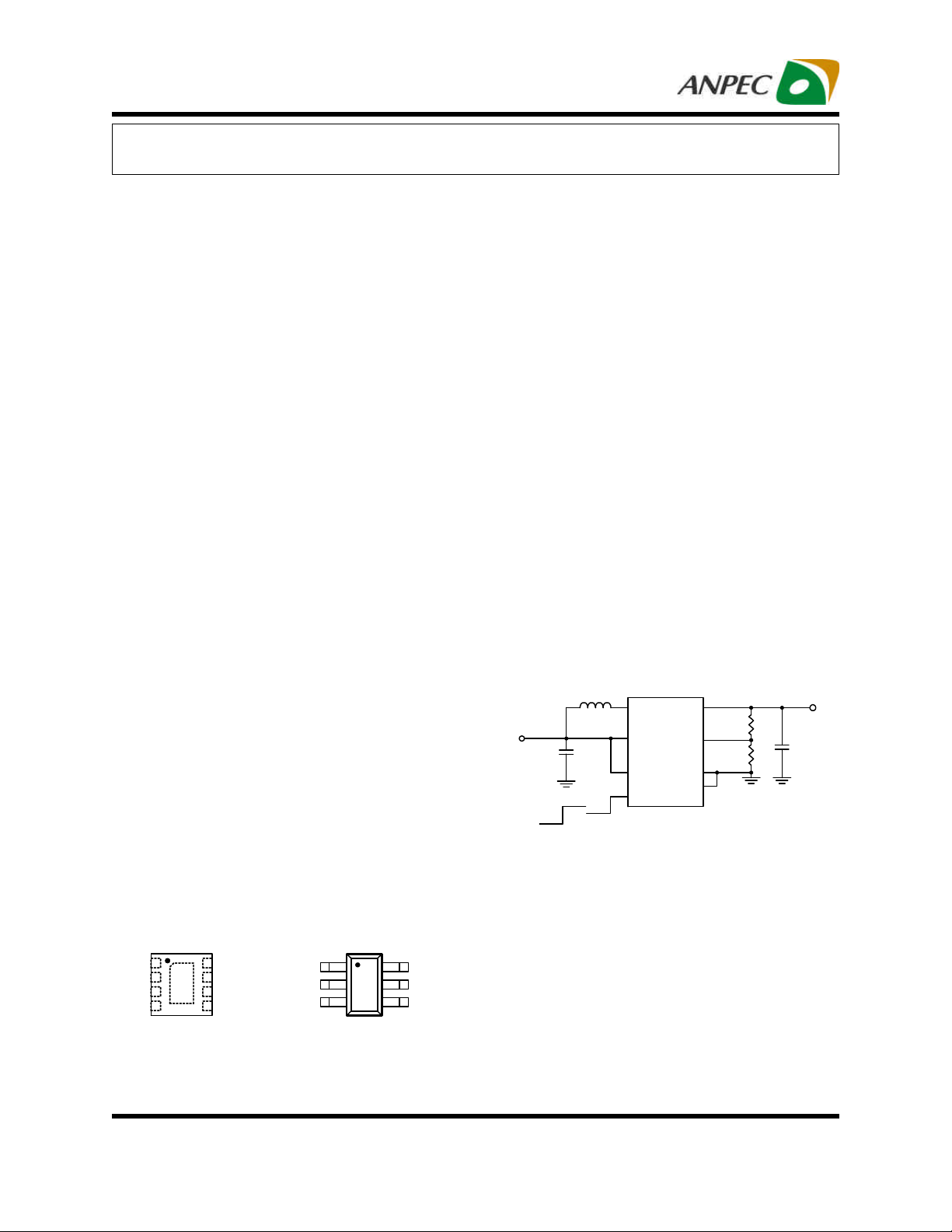
Simplified Application Circuit
V
C2
22µF
OUT
V
IN
0.8V to V
OUT
PFM/
PWM
C1
4.7µF
PWM
L1
4.7µH
8
SW
1
VIN
APW7212
3
EN
5
PS
VOUT
FB
GND
GND
2
R1
4
R2
6
7
Pin Configuration
1
VIN
2
VOUT
3
EN
FB
TDFN2x2-8
(Top View)
ANPEC reserves the right to make changes to improve reliability or manufacturability without notice, and
advise customers to obtain the latest version of relevant information to verify before placing orders.
Copyright ANPEC Electronics Corp.
Rev. A.2 - Feb., 2011
87SW
GND
6
GND
54
PS
SW 1
GND 2
FB 3
6 VIN
5 VOUT
4 EN
TSOT-23-6A
(Top View)
www.anpec.com.tw1
APW7212
Ordering and Marking Information
APW7212
Assembly Material
Handling Code
Temperature Range
Package Code
APW7212 QB:
APW7212 CT: W12X
Note: ANPEC lead-free products contain molding compounds/die attach materials and 100% matte tin plate termination finish; which
are fully compliant with RoHS. ANPEC lead-free products meet or exceed the lead-free requirements of IPC/JEDEC J-STD-020D for
MSL classification at lead-free peak reflow temperature. ANPEC defines “Green” to mean lead-free (RoHS compliant) and halogen
free (Br or Cl does not exceed 900ppm by weight in homogeneous material and total of Br and Cl does not exceed 1500ppm by
weight).
7212
X
Package Code
QB : TDFN2x2-8 CT : TSOT-23-6A
Operating Ambient Temperature Range
I : -40 to 85oC
Handling Code
TR : Tape & Reel
Assembly Material
G: Halogen and Lead Free Device
X - Date Code
X - Date Code
Absolute Maximum Ratings (Note 1)
Symbol
VIN VIN Supply Voltage (VIN to GND) -0.3 ~ 7 V
V
VOUT to GND Voltage -0.3 ~ 7 V
OUT
VSW SW to GND Voltage -0.3 ~ 7 V
FB, EN and PS to GND Voltage -0.3 ~ 7 V
TJ Maximum Junction Temperature 150 °C
T
Storage Temperature -65 ~ 150 °C
STG
T
Maximum Lead Soldering Temperature, 10 Seconds 260 °C
SDR
Note 1: Absolute Maximum Ratings are those values beyond which the life of a device may be impaired. Exposure to absolute
maximum rating conditions for extended periods may affect device reliability.
Parameter Rating Unit
Thermal Characteristics
Symbol
Thermal Resistance -Junction to Ambient
θJA
Note 2: θJA is measured with the component mounted on a high effective thermal conductivity test board in free air. The exposed pad
of package is soldered directly on the PCB.
Copyright ANPEC Electronics Corp.
Rev. A.2 - Feb., 2011
Parameter Typical Value Unit
(Note 2)
TDFN2x2-8
TSOT-23-6A
85
220
°C/W
www.anpec.com.tw2
APW7212
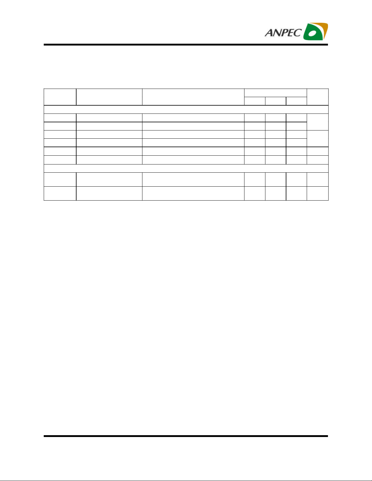
Recommended Operating Conditions (Note 3)
Symbol
VIN VIN Input Voltage 0.8 ~ V
EB, EN and PS to GND Voltage -0.3 ~ V
Parameter Range Unit
V
OUT
+0.3 V
OUT
L Inductor 1.5 ~ 10
CIN Input Capacitor 4.7 ~
C
Output Capacitor 3.7 ~
OUT
TA Ambient Temperature -40 ~ 85 °C
TJ Junction Temperature -40 ~ 125 °C
Note 3: Refer to the application circuit for further information.
Electrical Characteristics
Refer to the typical application circuits. These specifications apply over VIN = 1.2V, V
otherwise noted. Typical values are at TA = 25°C.
Symbol
Parameter Test Conditions
SUPPLY VOLTAGE AND CURRENT
Minimum Start-up Voltage
VIN
Minimum Operating Voltage after
Stat-up
V
Output Voltage Range 1.8 - 5.5 V
OUT
I
No Switching Quiescent Current
DD1
I
VIN Quiescent Current Measured from VIN, VIN = 1.2V, TA=25°C - 0.5 1
DD2
RL = 3kΩ
VEN = VIN - 0.8 0.9
Measured form VOUT, VFB = 1.3V,
V
= 3.3V, TA=25°C
OUT
ISD Shutdown Current VEN = GND, VIN = 1.2V - 0.1 1
REFERENCE AND OUTPUT VOLTAGES
V
Regulated Feedback Voltage
REF
TA = 0 ~ 85°C -1.5% 1.23 +1.5%
TA = -40 ~ 85°C -2% - +2%
IFB FB Input Current VFB = 1.3V -50 - 50 nA
INTERNAL POWER SWITCH
FSW Switching Frequency FB = GND 0.75
V
= 3.3V - 0.35
R
N-FET Switch On Resistance
N-FET
R
P-FET Switch On Resistance
P-FET
OUT
V
= 5V - 0.3 -
OUT
V
= 3.3V - 0.6 -
OUT
V
= 5V - 0.55
OUT
N-FET Switch Leakage Current VSW = 5V - 0.05
P-FET Switch Leakage Current VSW = 0V, V
I
N-FET Switch Current-Limit 0.9 1.2 - A
LIM
Dead-Time
D
SW Maximum Duty Cycle 80 85 95 %
MAX
(Note 4)
= 5V - 0.05
OUT
= 3.3V, I
OUT
= 0mA, TA = -40°C to 85°C, unless
OUT
APW7212
Min. Typ. Max.
- 1.05 1.15
- 40 60
1 1.25 MHz
-
1
1
- 10 - ns
µH
µF
µF
Unit
V
µA
µA
V
Ω
Ω
µA
µA
Copyright ANPEC Electronics Corp.
www.anpec.com.tw3
Rev. A.2 - Feb., 2011
APW7212
Electrical Characteristics (Cont.)
Refer to the typical application circuits. These specifications apply over VIN = 1.2V, V
otherwise noted. Typical values are at TA = 25°C.
= 3.3V, I
OUT
= 0mA, TA = -40°C to 85°C, unless
OUT
Symbol Parameter Test Conditions
APW7212
Min. Typ. Max.
CONTROL STAGE
EN EN Input Low Threshold - - 0.4
EN Input High Threshold 1 - -
PS PS Input Low Threshold - - 0.4
PS Input High Threshold 1 - IEN EN Input Leakage Current VEN = 5V or GND - 0.4 1
IPS PS Input Leakage Current VPS = 5V or GND - 0.1 1
OVER-TEMPERATURE PROTECTION
T
OTP
Note 4: Guaranteed by design, not production tested.
Over-Temperature
Protection
Over-Temperature
Protection Hysteresis
(Note 4)
(Note 4)
TJ Rising - 150 - °C
- 30 - °C
Unit
V
V
µA
µA
Copyright ANPEC Electronics Corp.
www.anpec.com.tw4
Rev. A.2 - Feb., 2011
APW7212
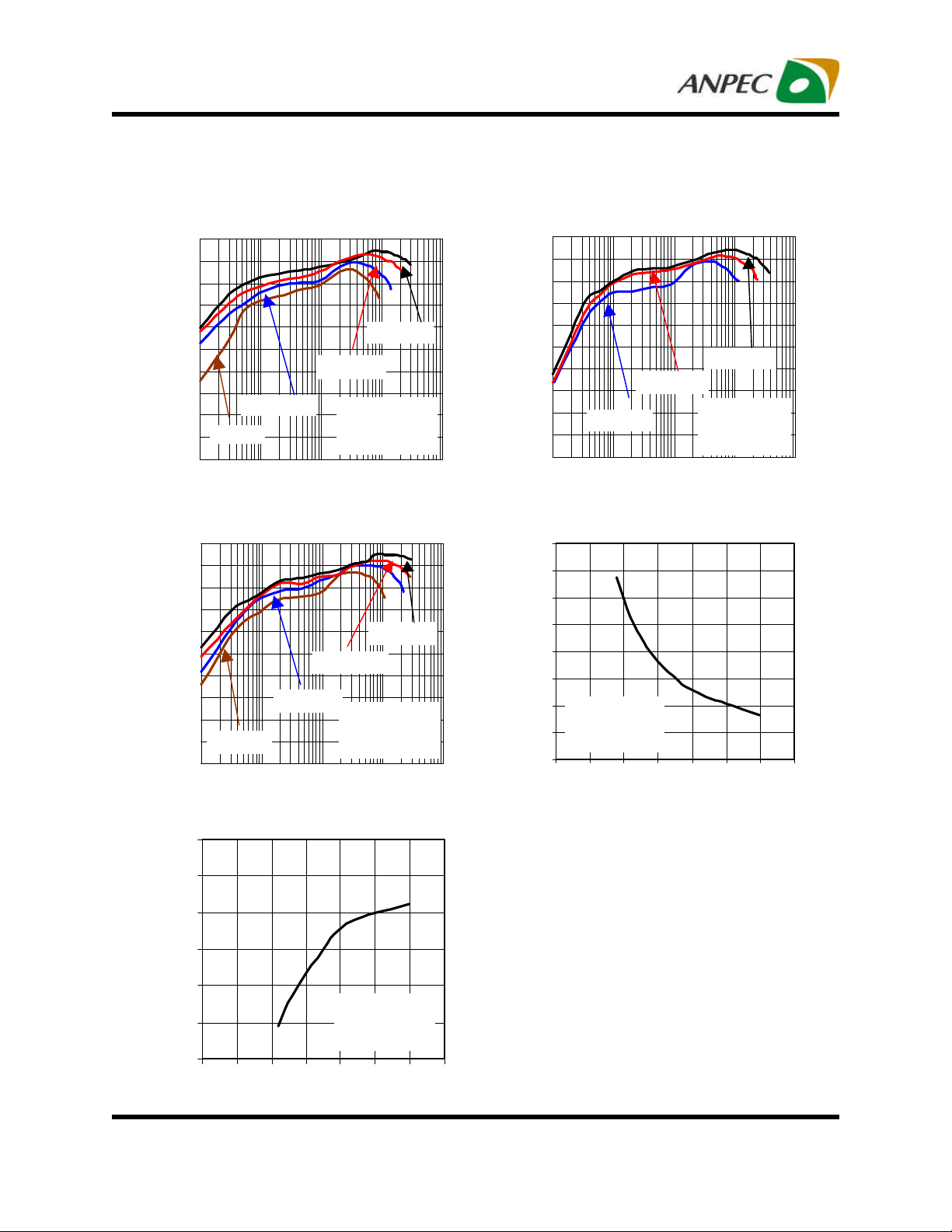
Typical Operating Characteristics
(Refer to the application circuit in the section"Typical Application Circuits", VIN=1.5V, V
otherwise specified )
100
90
80
70
60
50
40
Efficiency (%)
30
20
VIN=0.9V
10
0
0.1 1 10
100
90
80
70
60
50
40
Efficiency (%)
30
20
VIN=1.2V
10
0
0.1 1 10 100 1000
Start-up Voltage vs. Load Current
300
Efficiency vs. Load Current
VIN=2.4V
VIN=1.8V
.
VIN=1.2V
V
OUT
L = 4.7µH
C
OUT
= 3.3V
= 22µF
100
Load Current, I
OUT
(mA)
Efficiency vs. Load Current
VIN=3.6V
VIN=2.4V
VIN=1.8V
V
OUT
L = 4.7µH
C
= 22µF
OUT
Load Current, I
OUT
(mA)
= 5V
1000
100
90
80
70
60
50
40
Efficiency (%)
30
20
10
0
400
350
(uA)
300
IN
250
200
150
100
No Load Input Current, I
50
Efficiency vs. Load Current
VIN=1.2V
0.1
1 10 100 1000
Load Current, I
No Load Input Current vs. Supply
V
= 3.3V
OUT
L = 4.7µH
C
= 22µF
0
OUT
0 0.5 1 1.5 2 2.5 3 3.5
Supply Voltage, VIN(V)
=3.3V, TA=25oC unless
OUT
VIN=2.4V
VIN=1.8V
V
= 4V
OUT
L = 4.7µH
C
= 22µF
OUT
(mA)
OUT
Voltage
250
(mA)
200
OUT
150
100
Load Current, I
50
0
0 0.5 1 1.5 2 2.5 3 3.5
Start-up Voltage, V
Copyright ANPEC Electronics Corp.
Rev. A.2 - Feb., 2011
V
OUT
L = 4.7µH
C
OUT
(V)
IN
= 3.3V
= 22µF
www.anpec.com.tw5
APW7212
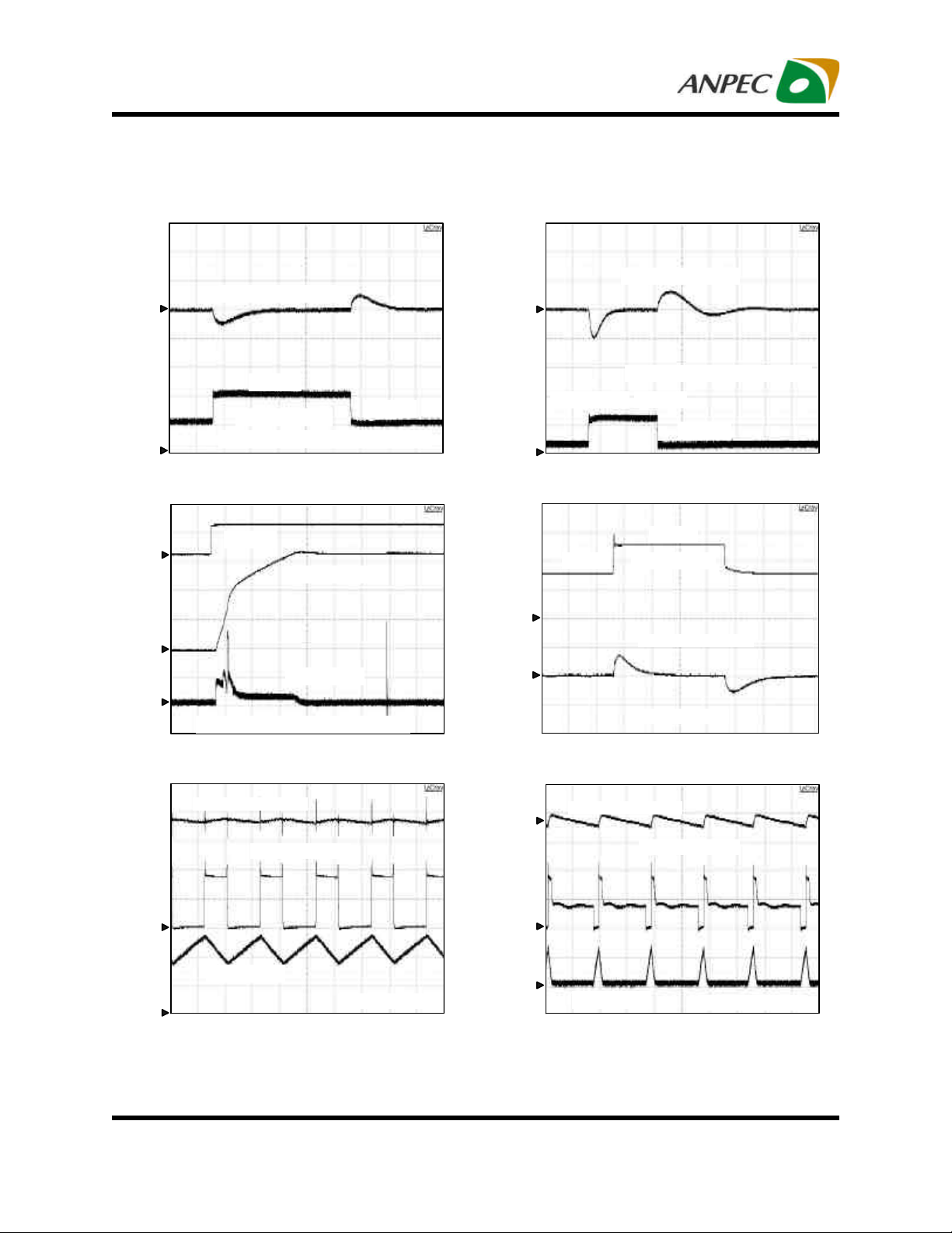
Operating Waveforms
(Refer to the application circuit in the section “Typical Application Circuits”, VIN=1.5V, V
otherwise specified)
Load Transient Response
V
,200mV/Div, AC
1
OUT
1
Load Transient Response
V
OUT
=3.3V,TA=25oC unless
OUT
,200mV/Div, AC
2
Time: 100µs/Div
1
2
3
Time: 500µs/Div
200mA
I
, 100mA/Div
OUT
L=4.7µH, VIN=1.5V, C
No Load Start-up
V
EN
V
, 1V/Div
OUT
IIN, 0.2A/Div
L=4.7µH, VIN=1.5V, I
OUT
Normal Operating Waveform
V
10mV/Div, AC
OUT,
VLX, 2V/Div, DC
100mA
=22µF
OUT
=0mA
OUT
2
Time: 100µs/Div
1
2
Time: 100µs/Div
1
L=4.7µH, VIN=1.5V, C
, 0.1A/Div
110mAI
10mA
Line Transient Response
2.5V
V
0.5V/Div1.5V
IN,
V
200mV/Div,AC
OUT,
I
= 100mA
OUT
Normal Operating Waveform
V
10mV/Div, AC
OUT,
VLX, 2V/Div, DC
OUT
=22µF
2
IL, 200mA/Div
3
Time: 500ns/Div
I
Copyright ANPEC Electronics Corp.
Rev. A.2 - Feb., 2011
= 200mA
OUT
2
3
Time: 10µs/Div
IL, 500mA/Div
I
OUT
= 20mA
www.anpec.com.tw6

APW7212
Pin Description
PIN
NO.
TDFN2x2-8 TSOT-23-6A
1 6 VIN Supply Voltage Input Pin.
2 5 VOUT Converter output and control circuitry bias supply pin.
3 4 EN
4 3 FB
5 - PS
6, 7 2 GND Power and signal ground pin.
8 1 SW Switch pin. Connect this pin to inductor.
- -
NAME
Exposed
PAD
Enable Control Input. Forcing this pin above 1.0V enables the device. Forcing this
pin below 0.4V to shut it down. In shutdown, all functions are disabled to decrease
the supply current below 1µA.
Feedback Input. The device senses feedback voltage via FB and regulate the
voltage at 1.23V. Connecting FB with a resistor-divider from the output set the
output voltage in the range from 1.8 to 5.5V.
Pulse Skipping Mode Selection. Pulling this pin to logic high to force boost converter
enter PWM mode. Pulling it low to automatic switch under PFM (Pulse Frequency
Mode) and PWM mode. Do not leave this pin floating. This pin internally connects to
GND for TSOT-23-6 package.
Connected this pad to GND.
FUNCTION
Copyright ANPEC Electronics Corp.
Rev. A.2 - Feb., 2011
www.anpec.com.tw7

APW7212
Block Diagram
EN
GND
Shutdown
Control
Over-
Temperature
Protection
Slope
Compensation
Oscillator
From
V
MAX
Control
Softstart
Σ
VIN
Low
Voltage
Start-up
Current-
limit
MUX
Logic Control
ICMP
COMP
V
MAX
Control
From VOUT
Error
Amplifier
EAMP
Zero-Crossing
Comparator
Gate
Control
Current Sense
Amplifier
V
REF
1.23V
PS
(APW7212CT only)
VOUT
SW
FB
Typical Application Circuit
L1
V
IN
0.8V to V
OUT
PFM/
PWM
Copyright ANPEC Electronics Corp.
Rev. A.2 - Feb., 2011
4.7µH
C1
4.7µF
PWM
8
SW
1
VIN
3
EN
5
PS
VOUT
APW7212
GND
GND
FB
V
2
OUT
R1
4
R2
C2
22µF
6
7
www.anpec.com.tw8

APW7212
Function Description
Main Control Loop
The APW7212 is a c onstant frequency, synchronous
rectifier, and current-mode switching regulator. In normal
operation, the internal N-channel power MOSFET is turned
on each cycle when the oscillator sets an internal RS
latch and turned off when an internal comparator (ICMP)
resets the latch. The peak inductor current which ICMP
resets the RS latch is controlled by the voltage on the
COMP node, whic h is the output of the error amplifier
(EAMP). An external resistive divider connected between
V
and ground allows the EAMP to rec eive an output
OUT
feedback voltage VFB at FB pin. When the load current
increases, it causes a slightly decrease in VFB relative to
the 1.23V reference, which in turn causes the COMP voltage to increase until the average inductor current matches
the new load current.
Start-up
A start-up oscillator circuit is integrated in the APW7212.
When the device enables, the circ uit pumps the output
voltage high. Once the output voltage reaches 1.6V (typ),
the main DC-DC circ uitry turns on and boosts the output
voltage to the final regulation voltage.
Automatic PFM/PWM mode Switch
The APW7212 is a fixed frequency PWM peak current
modulation control step-up converter. At light loads, the
APW7212 will automatically enter in pulse frequency
modulation operation to reduce the dominant switching
losses. In PFM operation, the inductor current may reach
zero or reverse on each pulse. A zero current comparator
turns off the P-channel synchronous MOSFET, forcing
DCM(Discontinuous Current Mode) operation at light load.
These controls get very low quiescent current, help to
maintain high efficiency over the complete load range.
Synchronous Rectification
The internal synchronous rectifier eliminates the need
for an external Schottky diode, thus reducing cost and
board space. During the cycle off-time, the P-FET turns
on and shunts the FET body diode. As a result, the synchronous rectifier significantly improves efficiency without the addition of an external component. Conversion
efficiency can be as high as 92%.
Load Disconnect
Driving EN to ground places the APW7212 in shutdown
mode. When in shutdown, the internal power MOSFET
turns off, all internal circuitry shuts down and the quiescent supply current reduces to 1µA maximum.
A special circuit is applied to disconnect the load from the
input during shutdown the converter. In conventional synchronous rectifier circuits, the back-gate diode of the highside P-FET is forward biased in shutdown and allows
current flowing from the battery to the output. However,
this device uses a special circuit, which takes the cathode of the back-gate diode of the high-side P-FET and
disconnects it from the source when the regulator is
shutdown. The benefit of this feature for the system design engineer is that the battery is not depleted during
shutdown of the converter. No additional components
must be added to the design to make sure that the battery is disconnected from the output of the converter.
Current-Limit Protection
The APW7212 monitors the inductor current, flowing
through the N-FET, and limits the current peak at currentlimit level to prevent loads and the APW7212 from damages during overload conditions.
Over-Temperature Protection (OTP)
The over-temperature circuit limits the junction temperature of the APW7212. When the junction temperature exceeds 150oC, a thermal sensor turns off the both N-FET
and P-FET, allowing the devices to cool. The thermal
sensor allows the converters to start a soft-start process
and regulate the output voltage again after the junction
temperature cools by 30oC. The OTP is designed with a
30oC hysteresis to lower the average Junction Temperature (TJ) during continuous thermal overload conditions,
increasing the lifetime of the device.
Copyright ANPEC Electronics Corp.
Rev. A.2 - Feb., 2011
www.anpec.com.tw9

APW7212
(
)
Application Information
Input Capacitor Selection
The input capacitor (CIN) reduces the current peaks drawn
from the input supply and reduces noise injection into
the IC. The reflected ripple voltage will be smaller with
larger CIN. For reliable operation, it is recommended to
select the capacitor voltage rating at least 1.2 times higher
than the maximum input voltage. The capacitors should
be placed close to the VIN and GND.
Inductor Selection
For high efficiencies, the inductor should have a low DC
resistance to minimize conduction losses. Especially at
high-switching frequencies the core material has a higher
impact on efficiency. When using small chip inductors,
the efficiency is reduced mainly due to higher inductor
core losses. This needs to be considered when selecting the appropriate inductor. The inductor value determines the inductor ripple current. The larger the inductor
value, the smaller the inductor ripple current and the lower
the conduction losses of the converter. Conversely, larger
inductor values cause a slower load transient response.
A reasonable starting point for setting ripple current, ∆IL,
is 30% to 50% of the average inductor current. The recommended inductor value can be calculated as below:
2
V
IN
≥
L
V
OUT
−
⋅
VV
⋅
IF
η
INOUT
⋅
∆
)MAX(OUTSW
I
L
I
( )
AVGL
where
VIN = input voltage
V
= output voltage
OUT
FSW = switching frequency in MHz
I
= maximum output current in amp.
OUT
η = Efficiency
∆IL /I
= (0.3 to 0.5 typical)
L(AVG)
The peak inductor current is calculated as below:
VVV
1
II
I
V
I
IN
IN
C
IN
I
L
I
SW
I
D
L
)MAX(INPEAK
2
N-FET
⋅+=
LX
−⋅
INOUTIN
FLV
⋅⋅
SWOUT
I
D1
I
SW
I
PEAK
I
IN
OUT
ESR
C
OUT
V
OUT
I
LIM
∆I
L
I
OUT
Output Capacitor Selection
The current-mode c ontrol scheme of the APW7212 allows the use of tiny ceramic capacitors . The higher capacitor value provides the good load transients response.
Ceramic capacitors with low ESR values have the lowest
output voltage ripple and are recommended. If required,
tantalum capacitors may be used as well. The output ripple
is the sum of the voltages across the ESR and the ideal
output capacitor.
To avoid saturation of the inductor, the inductor should be
rated at least for the maximum input current of the con-
V
COUT
I
OUT
⋅≅∆
C
OUT
−
VV
INOUT
⋅
FV
SWOUT
verter plus the inductor ripple current. The maximum in-
ΔV
= ΔV
put current is calculated as below:
⋅
VI
=
I
)MAX(IN
OUT)MAX(OUT
η⋅
V
IN
OUT
Copyright ANPEC Electronics Corp.
Rev. A.2 - Feb., 2011
RIV ⋅≅∆
ESR
ESRPEAKESR
+ ΔV
COUT
www.anpec.com.tw10

APW7212
Application Information (Cont.)
Output Capacitor Selection (Cont.)
Where I
is the peak inductor current. For ceramic ca-
PEAK
pacitor application, the output voltage ripple is dominated
by the ∆V
. When choosing the input and output ce-
COUT
ramic capacitors, the X5R or X7R with their good temperature and voltage characteristics are recommended.
Output Voltage Setting
A resistive divider sets the output voltage. The external
resistive divider is connected to the output, allowing remote voltage sensing as shown in “Typical Application
Circuits”. A suggestion of the maximum value of R1 is
2MΩ and R2 is 600kΩ to keep the minimum current that
provides enough noise rejection ability through the resistor divider. The output voltage can be calculated as
below:
1R
+⋅=
1VV
REFOUT
2R
1R
+=
123.1
2R
Layout Consideration
For all switching power supplies, the layout is an important step in the design, especially at high peak currents
and switching frequencies. If the layout is not done
carefully, the regulator may show noise problems and
duty cycle jitter.
Layout Consideration
Via to VIN
1
VOUT
2
3
R1
APW7212 Layout Suggestion
V
IN
L1
SW
R2
Via To V
APW7212 Layout Suggestion
VIN
C1C2
C2
L1
PWM
PFM/PWM
Via To V
IN
V
EN
V
OUT
8
SW
7
GND
6
GND
54
PS
R2
C1
GND
FB
GND
R1
OUT
1. Since the VOUT supplies IC bias voltage, the output
capacitor should be placed close to the VOUT and
GND. Connecting the capacitor with VOUT and GND
pins by short and wide tracks without using any via
holes for good filtering and minimizing the voltage
ripple.
2. To minimize copper trace connections that can inject
noise into the system, the inductor should be placed
as close as possible to the SW pin to minimize the
noise coupling into other circuits.
3. Since the feedback pin and network is a high impedance circuit the feedback network should be routed
away from the inductor. The feedback pin and feedback network should be shielded with a ground plane
or trace to minimize noise coupling into this circuit.
4. A star ground connection or ground plane minimizes
ground shifts and noise is recommended.
Copyright ANPEC Electronics Corp.
Rev. A.2 - Feb., 2011
www.anpec.com.tw11

APW7212
Pack age Information
TDFN2x2-8
D
D2
Pin 1 Corner
A
E
b
A1
A3
E2
K
S
Y
M
B
O
L
A
A1
A3
b
D
D2
E
E2
e
L
K 0.20
Note : 1. Followed from JEDEC MO-229 WCCD-3.
Copyright ANPEC Electronics Corp.
Rev. A.2 - Feb., 2011
MIN. MAX.
0.70
0.00
0.18 0.30
1.90 2.10
1.00 1.60
1.90 2.10
0.60
0.30 0.45
L
e
TDFN2x2-8
MILLIMETERS
0.80
0.05
0.20 REF
1.00
0.50 BSC 0.020 BSC
INCHES
MIN. MAX.
0.028
0.000
0.008 REF
0.007 0.012
0.075 0.083
0.039 0.063
0.075 0.083
0.024
0.012 0.018
0.008
0.031
0.002
0.039
www.anpec.com.tw12

APW7212
Pack age Information
TSOT-23-6A
D
e
SEE VIEW A
E1
E
b
e1
A
A2A1
L
VIEW A
S
Y
M
B
O
L
A
A1
A2
b
c
D
E
E1
e
e1
θ
Note : Dimension D and E1 do not include mold flash, protrusions or gate
burrs. Mold flash, protrusion or gate burrs shall not exceed 10 mil
per side.
MILLIMETERS
MIN.
0.70
0.01
0.70
0.30
0.08
2.70 3.10
2.60 3.00
1.40 1.80
0.95 BSC
1.90 BSC
0.30L
0°
TSOT-23-6A
INCHES
MAX.
1.00
0.10
0.90
0.50
0.20
0.60
8° 0° 8°
MIN.
0.028
0.000
0.028
0.012
0.003
0.106 0.122
0.102 0.118
0.055 0.071
0.037 BSC
0.075 BSC
0.012
MAX.
0.039
0.004
0.035
0.020
0.008
0.024
c
0.25
GAUGE PLANE
SEATING PLANE
Copyright ANPEC Electronics Corp.
Rev. A.2 - Feb., 2011
www.anpec.com.tw13

APW7212
Carrier Tape & R eel Dimensions
OD0
B0
P0
P2
P1
A
E1
F
W
Application
TDFN2x2-8
Application
TSOT-23-6A
K0
SECTION A-A
B
A
H
A0
SECTION B-B
OD1
B
T
A
d
T1
A H T1 C d D W E1 F
178.0±2.00 50 MIN.
8.4+2.00
-0.00
13.0+0.50
-0.20
1.5 MIN. 20.2 MIN. 8.0±0.20 1.75±0.10 3.50±0.05
P0 P1 P2 D0 D1 T A0 B0 K0
4.0±0.10 4.0±0.10 2.0±0.05
1.5+0.10
-0.00
1.5 MIN.
0.6+0.00
-0.4
3.35 MIN 3.35 MIN 1.30±0.20
A H T1 C d D W E1 F
178.0±2.00 50 MIN.
8.4+2.00
-0.00
13.0+0.50
-0.20
1.5 MIN. 20.2 MIN. 8.0±0.30 1.75±0.10 3.5±0.05
P0 P1 P2 D0 D1 T A0 B0 K0
4.0±0.10 4.0±0.10 2.0±0.05
1.5+0.10
-0.00
1.0 MIN.
0.6+0.00
-0.40
3.20±0.20 3.10±0.20 1.50±0.20
Copyright ANPEC Electronics Corp.
Rev. A.2 - Feb., 2011
(mm)
www.anpec.com.tw14

APW7212
Devices Per Unit
Package Type Unit Quantity
TDFN2x2-8
TSOT-23-6A
Taping Direction Information
TDFN2x2-8
Tape & Reel 3000
Tape & Reel 3000
USER DIRECTION OF FEED
TSOT-23-6
AAAX AAAX AAAX AAAX AAAX AAAX AAAX
Copyright ANPEC Electronics Corp.
Rev. A.2 - Feb., 2011
USER DIRECTION OF FEED
www.anpec.com.tw15

APW7212
Classification Profile
Classification Reflow Profiles
Profile Feature Sn-Pb Eutectic Assembly Pb-Free Assembly
Preheat & Soak
Temperature min (T
Temperature max (T
Time (T
smin
to T
smax
smin
smax
) (ts)
)
)
Average ramp-up rate
(T
to TP)
smax
Liquidous temperature (TL)
Time at liquidous (tL)
Peak package body Temperature
(Tp)*
See Classification Temp in table 1 See Classification Temp in table 2
Time (tP)** within 5°C of the specified
classification temperature (Tc)
Average ramp-down rate (Tp to T
smax
)
Time 25°C to peak temperature
* Tolerance for peak profile Temperature (Tp) is defined as a supplier minimum and a user maximum.
** Tolerance for time at peak profile temperature (tp) is defined as a supplier minimum and a user maximum.
Copyright ANPEC Electronics Corp.
Rev. A.2 - Feb., 2011
100 °C
150 °C
60-120 seconds
150 °C
200 °C
60-120 seconds
3 °C/second max. 3 °C/second max.
183 °C
60-150 seconds
217 °C
60-150 seconds
20** seconds 30** seconds
6 °C/second max. 6 °C/second max.
6 minutes max. 8 minutes max.
www.anpec.com.tw16

APW7212
Classification Reflow Profiles (Cont.)
Table 1. SnPb Eutectic Process – Classification Temperatures (Tc)
Package
Thickness
<2.5 mm
≥2.5 mm 220 °C 220 °C
Table 2. Pb-free Process – Classification Temperatures (Tc)
Package
Thickness
<1.6 mm
1.6 mm – 2.5 mm
≥2.5 mm 250 °C 245 °C 245 °C
Volume mm3
<350
260 °C 260 °C 260 °C
260 °C 250 °C 245 °C
Volume mm
<350
235 °C 220 °C
Reliability Test Program
Test item Method Description
SOLDERABILITY JESD-22, B102
HOLT JESD-22, A108
PCT JESD-22, A102
TCT JESD-22, A104
HBM MIL-STD-883-3015.7
MM JESD-22, A115
Latch-Up JESD 78
3
Volume mm3
350-2000
5 Sec, 245°C
1000 Hrs, Bias @ Tj=125°C
168 Hrs, 100%RH, 2atm, 121°C
500 Cycles, -65°C~150°C
VHBM≧2KV
VMM≧200V
10ms, 1tr≧100mA
Volume mm
≥350
Volume mm3
>2000
3
Customer Service
Anpec Electronics Corp.
Head Office :
No.6, Dusing 1st Road, SBIP,
Hsin-Chu, Taiwan, R.O.C.
Tel : 886-3-5642000
Fax : 886-3-5642050
Taipei Branch :
2F, No. 11, Lane 218, Sec 2 Jhongsing Rd.,
Sindian City, Taipei County 23146, Taiwan
Tel : 886-2-2910-3838
Fax : 886-2-2917-3838
Copyright ANPEC Electronics Corp.
Rev. A.2 - Feb., 2011
www.anpec.com.tw17

 Loading...