

APW7209
1MHz, High-Efficiency, Step-Up Converter for 2 to 10 White LEDs
Features
• Wide Input Voltage from 2.5V to 6V
• 0.3V Reference Voltage
• Fixed 1MHz Switching Frequency
• High Efficiency up to 88%
• 100Hz to 200kHz PWM Brightness Control
Frequency
• Open-LED Protection
• Under-Voltage Lockout Protection
• Over-Temperature Protection
• <1µA Quiescent Current during Shutdown
• SOT-23-6 and TSOT-23-6A Package
• Lead Free and Green Devices Available
(RoHS Compliant)
Applications
• White LED Display Backlighting
• Cell Phone and Smart Phone
General Description
The APW7209 is a current-mode and fixed frequency
boost converter with an integrated N-FET to drive up to 10
white LEDs in series.
The series connection allows the LED current to be identical for uniform brightness. Its low on-resistance of NFET and low feedback voltage reduce power loss and
achieve high effic iency. Fast switching frequency(1MHz
typical) allows us ing small-size inductor and both of input and output capacitors. An over-voltage protec tion
function, which monitors the output voltage via OVP pin,
stops switching of the IC if the OVP voltage exceeds the
over voltage threshold. An internal soft-start circuit eliminates the inrush c urrent during start-up.
The APW7209 also integrates under-voltage lockout, overtemperature protection, and c urrent limit circuits to protect the IC in abnormal conditions.The APW7209 is available in a SOT-23-6 and TSOT-23-6 package.
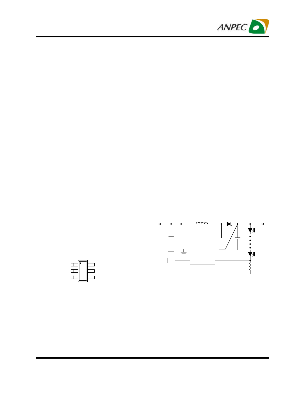
Simplified Application Circuit
• PDA, PMP, MP3
• Digital Camera
Pin Configuration
LX 1
GND 2
FB 3
SOT-23-6/TSOT-23-6
(Top View )
ANPEC reserves the right to make changes to improve reliability or manufacturability without notice, and
advise customers to obtain the latest version of relevant information to verify before placing orders.
6 VIN
5 OVP
4 EN
V
IN
C1
4.7µF
OFF ON
22µH
6
VIN
2
GND
APW7209
4
EN
L1
LX
OVP
FB
V
OUT
1
5
3
C2
1µF
Up to 10
WLEDs
R1
15Ω
Copyright ANPEC Electronics Corp.
Rev. A.8 - Sep., 2013
www.anpec.com.tw1
APW7209
Ordering and Marking Information
APW7209
Assembly Material
Handling Code
Temperature Range
Package Code
APW7209 C: X - Date Code
Note: ANPEC lead-free products contain molding compounds/die attach materials and 100% matte tin plate termination finish; which
are fully compliant with RoHS. ANPEC lead-free products meet or exceed the lead-free requirements of IPC/JEDEC J-STD-020D for
MSL classification at lead-free peak reflow temperature. ANPEC defines “Green” to mean lead-free (RoHS compliant) and halogen
free (Br or Cl does not exceed 900ppm by weight in homogeneous material and total of Br and Cl does not exceed 1500ppm by
weight).
W09X
Package Code
C : SOT-23-6 CT : TSOT-23-6A
Operating Ambient Temperature Range
I : -40 to 85 oC
Handling Code
TR : Tape & Reel
Assembly Material
G : Halogen and Lead Free Device
APW7209 CT: X - Date Code
W09X
Absolute Maximum Ratings (Note 1)
Symbol
VIN VIN Supply Voltage (VIN to GND) -0.3 ~ 7 V
FB, EN to GND Voltage -0.3 ~ VIN V
VLX LX to GND Voltage -0.3 ~ 42 V
V
OVP to GND Voltage -0.3 ~ 42 V
OVP
TJ Maximum Junction Temperature 150 °C
T
Storage Temperature -65 ~ 150 °C
STG
T
Maximum Lead Soldering Temperature, 10 Seconds 260 °C
SDR
Note1: Stresses beyond those listed under "absolute maximum ratings" may cause permanent damage to the device. These are
stress ratings only and functional operation of the device at these or any other conditions beyond those indicated under "recommended operating conditions" is not implied. Exposure to absolute maximum rating conditions for extended periods may affect device
reliability.
Parameter Rating Unit
Thermal Characteristics (Note 2)
Symbol
Junction to Ambient Thermal Resistance.
θJA
Note 2: θJA is measured with the component mounted on a high effective thermal conductivity test board in free air.
Recommended Operating Conditions (Note 3)
Parameter Typical Value Unit
SOT-23-6
TSOT-23-6A
250
220
°C/W
Symbol
VIN VIN Input Voltage 2.5~ 6 V
V
Converter Output Voltage Up to 37 V
OUT
CIN Input Capacitor 4.7 or higher
C
Output capacitor 0.68 or higher
OUT
L1 Inductor 6.8 ~ 47
TA Ambient Temperature -40 ~ 85 °C
TJ Junction Temperature -40 ~ 125 °C
Note 3: Refer to the application circuit for further information.
Copyright ANPEC Electronics Corp.
Rev. A.8 - Sep., 2013
Parameter Range Unit
µF
µF
µH
www.anpec.com.tw2
APW7209
Electrical Characteristics
(Refer to figure 1 in the “Typical Application Circuits”. These specifications apply over VIN = 3.6V, TA = -40°C to 85°C, unless otherwise
noted. Typical values are at TA = 25°C.)
Symbol
Parameter Test Conditions
APW7209
Min. Typ. Max.
SUPPLY VOLTAGE AND CURRENT
VIN Input Voltage Range TA = -40 ~ 85°C, TJ = -40 ~ 125°C 2.5 - 6 V
I
V
DD1
I
Input DC bias current
FB = GND, switching - 1 2 mA
DD2
ISD
= 0.4V, no switching 70 100 130 µA
FB
EN = GND - - 1 µA
UNDER VOLTAGE LOCKOUT
UVLO Threshold Voltage VIN Rising 2.0 2.2 2.4 V
UVLO Hysteresis Voltage 50 100 150 mV
REFERENCE AND OUTPUT VOLTAGES
V
Regulated Feedback Voltage
REF
TA = 25°C 0.285
TA = -40 ~ 85°C (TJ = -40 ~ 125°C) 0.276
0.3 0.315
- 0.324
IFB FB Input Current -50 - 50 nA
INTERNAL POWER SWITCH
FSW Switching Frequency FB=GND 0.8 1.0 1.2 MHz
RON Power Switch On Resistance - 0.6 -
I
Power Switch Current Limit 0.7 1.0 1.4 A
LIM
LX Leakage Current VEN=0V, VLX=0V or 5V, VIN = 5V -1 - 1 µA
D
LX Maximum Duty Cycle 92 95 98 %
MAX
OUTPUT OVER-VOLTAGE PROTECTION
V
Over Voltage Threshold V
OVP
rising 38 40 43 V
OVP
OVP Hysteresis - 3 - V
OVP Leakage Current V
=40V - 50 - µA
OVP
ENABLE AND SHUTDOWN
V
EN Voltage Threshold VEN Rising 0.4 0.7 1 V
TEN
EN Voltage Hysteresis - 0.1 - V
I
EN Leakage Current VEN= 0~5V, VIN = 5V -1 - 1 µ A
LEN
OVER-TEMPERATURE PROTECTION
T
Over-Temperature Protection
OTP
Over-Temperature Protection
Hysteresis
(Note 4)
(Note 4)
TJ Rising - 150 - °C
- 40 - °C
Note 4: Guaranteed by design, not production tested.
Unit
V
Ω
Copyright ANPEC Electronics Corp.
www.anpec.com.tw3
Rev. A.8 - Sep., 2013
APW7209
≅
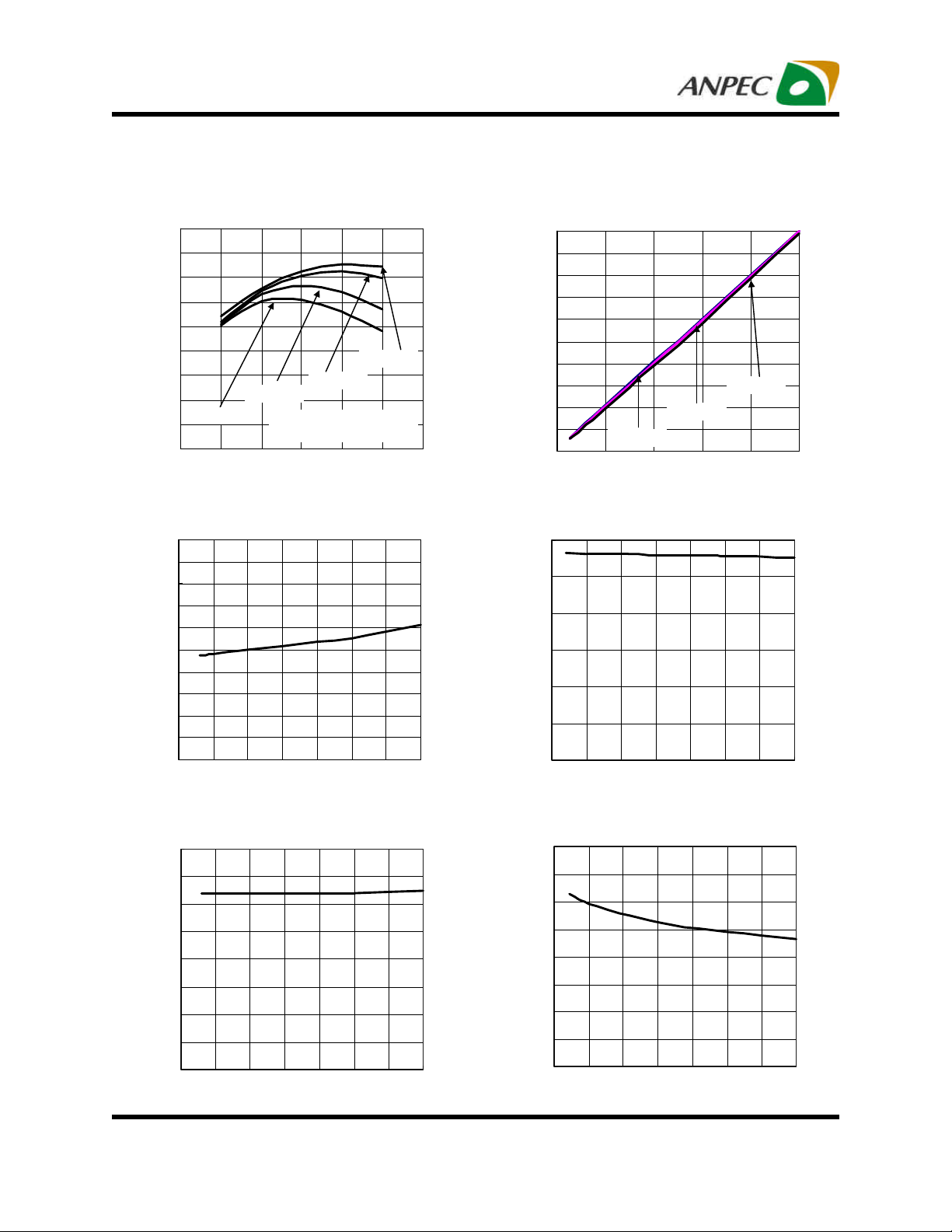
Typical Operating Characteristics
(Refer to figure 1 in the section “Typical Application Circuits”, VIN=3.6V, TA=25oC, 10WLEDs unless otherwise specified)
Efficiency vs. WLED Current
95
90
85
80
75
70
Efficiency (η)
65
60
VIN=3.3V
55
50
0 5 10 15 20 25 30
VIN=3.6V
WLED Current, I
VIN=4.2V
10 WLEDs 33V@20mA
(mA)
LED
WLED Current vs. Supply Voltage
21.0
20.8
20.6
20.4
(mA)
LED
20.2
20.0
19.8
19.6
WLED Current, I
19.4
19.2
19.0
2.5 3 3.5 4 4.5 5 5.5 6
Supply Voltage, V
IN
Switching Frequency vs. Supply
1.2
1.1
(MHz)
1
SW
0.9
0.8
0.7
0.6
0.5
Switching Frequency, F
0.4
2.5 3 3.5 4 4.5 5 5.5 6
Copyright ANPEC Electronics Corp.
Rev. A.8 - Sep., 2013
Voltage
Supply Voltage, V
IN
(V)
(V)
η=P
VIN=5V
OUT/PIN
WLED Current vs. PWM Duty Cycle
20
18
16
14
(mA)
LED
12
10
8
6
WLED Current, I
4
2
0
0 20 40 60 80 100
100Hz
1kHz
PWM Duty Cycle (%)
Maximum Duty Cycle vs. Supply
Voltage
100
90
(%)
MAX
80
70
60
50
Maximum Duty Cycle, D
40
2.5 3 3.5 4 4.5 5 5.5 6
Supply Voltage, V
IN
Switch ON Resistance vs. Supply
0.8
0.7
(Ω)
ON
0.6
0.5
0.4
0.3
0.2
0.1
Switch ON Resistance, R
0
2.5 3 3.5 4 4.5 5 5.5 6
Voltage
Supply Voltage, V
IN
100kHz
(V)
(V)
www.anpec.com.tw4
APW7209
Operating Waveforms
(Refer to the application circuit in the section “Typical Application Circuits”, VIN=3.6V, TA=25oC, 10WLEDs unless otherwise
specified )
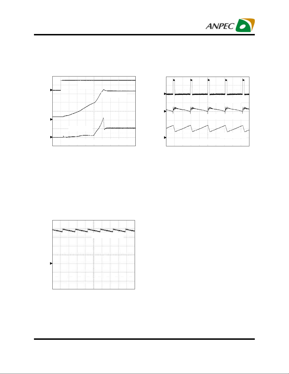
1
2
3
CH1: VEN, 1V/Div, DC
CH2: V
OUT
CH3: IIN, 0.2A/Div, DC
Time: 0.5ms/Div
Start-up
V
EN
V
, 10V/Div
OUT
IIN, 0.2A/Div
10WLEDs, L=22µH, VIN=3.6V, I
, 10V/Div, DC
LED
=20mA
Normal Operating Waveform
1
2
3
CH1: VLX, 20V/Div, DC
CH2: V
OUT
CH3: IL, 0.2A/Div, DC
Time: 500ns/Div
VLX, 20V/Div, DC
V
, 100mV/Div, AC
OUT
IL, 0.2A/Div
10WLEDs, L=22µH, VIN=3.6V, I
, 100mV/Div, AC
LED
=20mA
Open-LED Protection
V
, 10V/Div
OUT
1
CH1: V
Time: 20ms/Div
Copyright ANPEC Electronics Corp.
Rev. A.8 - Sep., 2013
, 10V/Div, DC
OUT
www.anpec.com.tw5
APW7209
Σ
Pin Description
PIN
NO. NAME
1 LX Switch pin. Connect this pin to inductor/diode here.
2 GND Power and signal ground pin.
3 FB
4 EN
5 OVP Over Voltage Protection Input Pin. OVP is connected to the output capacitor of the converter.
6 VIN Main Supply Pin. Must be closely decoupled to GND with a 4.7µ F or greater ceramic capacitor.
Feedback Pin. Reference voltage is 0.3V(typical). Connect this pin to cathode of the lowest LED
and current-sense resistor (R1). Calculate resistor value according to R1=0.3V/I
Enable Control Input. Forcing this pin above 1.0V enables the device, or forcing this pin below 0.4V
to shut it down. In shutdown, all functions are disabled to decrease the supply current below 1µA.
Do not leave this pin floating.
FUNCTION
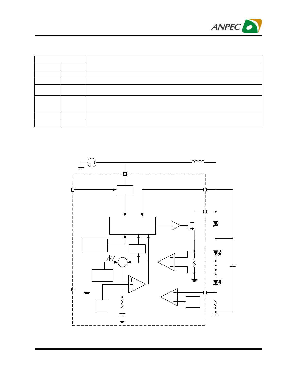
Block Diagram
VIN
EN
UVLO
OVP
LED
.
GND
Over-
Temperature
Protection
Slope
Compensation
Oscillator
Soft-
start
Control Logic
Current
limit
ICMP
COMP
Gate Driver
Current Sense
Amplifier
Error
Amplifier
EAMP
V
REF
0.3V
LX
FB
Copyright ANPEC Electronics Corp.
Rev. A.8 - Sep., 2013
www.anpec.com.tw6

APW7209
Typical Application Circuits
V
IN
C1
4.7µF
OFF ON
V
IN
C1
4.7µF
100Hz~200kHz
Duty=100%, I
LED
Duty=0%, LED off
L1
22µH
6
VIN
2
GND
4
EN
APW7209
LX
OVP
FB
1
5
3
Figure 1. Typical 10 WLEDs Application
L1
22µH
=20mA
6
VIN
2
GND
4
EN
APW7209
LX
OVP
FB
1
5
3
C2
1µF
C2
1µF
V
Up to 10
WLEDs
R1
15Ω
V
Up to 10
WLEDs
R1
15Ω
OUT
OUT
Figure 2. Brightness control by using a PWM signal applied to EN
V
IN
L1
22µH
C1
4.7µF
1R
OFF ON
brightness
V2R
REF
=
PWM
control
⋅=
1V
+⋅
6
VIN
2
GND
APW7209
4
EN
3.3V
Duty=100%, LED off
Duty=0%, I
2R
I
LED
V
⋅−
3R2R3R
MAX,LED
=22mA
MIN,ADJREF
0V
LX
OVP
FB
1
5
C2
1µF
Up to 10
WLEDs
3
R2
R3
100K
V
ADJ
R4
10K
C3
0.1µF
V3RIV3RI
−⋅−+⋅
MAX,ADJMIN,LEDMIN,ADJMAX,LED
10K
IVIVIVIV
⋅−⋅−⋅+⋅
R1
15Ω
MAX,LEDREFMIN,LEDMIN,ADJMIN,LEDREFMAX,LEDMAX,ADJ
Figure 3. Brightness control using a filtered PWM signal
V
OUT
Copyright ANPEC Electronics Corp.
Rev. A.8 - Sep., 2013
www.anpec.com.tw7

APW7209
Function Description
Main Control Loop
The APW7209 is a constant frequency current-mode
switching regulator. During normal operation, the internal N-channel power MOSFET is turned on each cycle
when the oscillator sets an internal RS latch and turned
off when an internal comparator (ICMP) resets the latch.
The peak inductor current at which ICMP resets the RS
latch is controlled by the voltage on the COMP node, which
is the output of the error amplifier (EAMP). An external
current-sense resistor connected between cathode of the
lowest LED and ground allows the EAMP to receive a
current feedback voltage VFB at FB pin. When the LEDs
voltage increases to cause the LEDs current to decrease,
it causes a slightly decrease in VFB relative to the 0.3V
reference, which in turn causes the COMP voltage to increase until the LEDs current reaches the set point.
VIN Under-Voltage Lockout (UVLO)
The Under-Voltage Lockout (UVLO) circuit compares the
input voltage at VIN with the UVLO threshold (2.2V rising,
typical) to ensure the input voltage is high enough for
reliable operation. The 100mV (typ) hysteresis prevents
supply transients from causing a restart. Once the input
voltage exceeds the UVLO rising threshold, startup begins.
When the input voltage falls below the UVLO falling
threshold, the controller turns off the converter.
Soft-Start
The APW7209 has a built-in soft-start to control the Nchannel MOSFET current rise during start-up. During softstart, an internal ramp voltage, connected to one of the
inverting inputs of the comoarator ICMP, raise up to replace the output voltage of error amplifier until the ramp
voltage reaches the V
Current-Limit Protection
The APW7209 monitors the inductor current, flowing
through the N-channel MOSFET, and limits the current
peak at current-limit level to prevent loads and the
APW7209 from damages in overload conditions.
COMP
.
Over-Temperature Protection (OTP)
The over-temperature circuit limits the junction temperature of the APW7209. When the junction temperature exceeds 150oC, a thermal sensor turns off the power
MOSFET, allowing the device to cool. The thermal s ensor allows the converter to start a soft-start process and
regulate the LEDs current again after the junc tion temperature cools by 40oC. The OTP is designed with a 40oC
hysteresis to lower the average Junction Temperature
(TJ) during continuous thermal overload conditions, increasing the lifetime of the device.
Enable/Shutdown
Driving EN to ground places the APW7209 in shutdown
mode. When in s hutdown, the internal power MOSFET
turns off, all internal circuitry shuts down and the quiescnet
supply current reduces to 1µA maximum.
This pin also could be used as a digital input allowing
brightness controlled by using a PWM signal with frequency from 100Hz to 200kHz. The 0% duty cycle of PWM
signal corresponds to zero LEDs current and 100% corresponds to full one.
Open-LED Protection
In driving LED applications, the feedback voltage on FB
pin falls down if one of the LEDs, in series, is failed.
Meanwhile, the c onverter unceasingly boosts the output
voltage like a open-loop operation. Therefore, an overvoltage protection (OVP), monitoring the output voltage
via OVP pin, is integrated into the chip to prevent the LX
and the output voltages from exceeding their maximum
voltage ratings. When the voltage on the OVP pin ris es
abov e the OVP threshold (40V, typical), the converter
stops switching and prevents the output voltage from
rising. The converter can work again when the falling OVP
voltage falls below the OVP voltage threshold.
Copyright ANPEC Electronics Corp.
Rev. A.8 - Sep., 2013
www.anpec.com.tw8

APW7209
(
)
Application Information
Input Capacitor Selection
The input c apacitor (CIN) reduces the ripple of the input
current drawn from the input supply and reduces nois e
injection into the IC. The reflected ripple voltage will be
smaller when an input capacitor with larger capacitance
is used. For reliable operation, it is recommended to
select the capacitor with maximum voltage rating at least
1.2 times of the maximum input voltage. The capacitors
should be placed close to the VIN and GND.
Inductor Selection
Selecting an inductor with low dc resistance reduces conduction losses and achieves high efficiency. The efficiency
is moderated whilst using small chip inductor which operates with higher inductor core los ses. Therefore, it is
necessary to take further consideration while choos ing
an adequate inductor. Mainly, the inductor value determines the inductor ripple current: larger inductor value
results in s maller inductor ripple current and lower conduction losses of the converter. However, larger inductor
value generates slower load transient response. A reasonable design rule is to set the ripple current, ∆IL, to be
30% to 50% of the maximum average inductor current,
I
. The inductor value can be obtained as below,
L(AVG)
2
V
IN
≥
L
×
V
OUT
−
VV
INOUT
×
IF
η
×
)MAX(OUTSW
I
( )
∆
I
L
AVGL
where
VIN = input voltage
V
= output voltage
OUT
FSW = switching frequency in MHz
I
= maximum output current in amp.
OUT
η = Efficiency
∆IL /I
= inductor ripple current/average current
L(AVG)
(0.3 to 0.5 typical)
To avoid saturation of the inductor, the inductor should be
rated at least for the maximum input c urrent of the converter plus the inductor ripple current. The maximum input current is calculated as below:
×
VI
=
I
)MAX(IN
OUT)MAX(OUT
η×
V
IN
The peak inductor current is calculated as the following
equation:
VVV21
−⋅
LX
INOUTIN
FLV
⋅⋅
SWOUT
D1
I
SW
I
PEAK
I
V
OUT
OUT
ESR
C
OUT
I
LIM
∆I
L
I
IN
I
OUT
II
V
I
IN
IN
C
IN
I
L
I
SW
I
D
⋅+=
)MAX(INPEAK
I
L
N-FET
Output Capacitor Selection
The current-mode control scheme of the APW7209 allows the us age of tiny ceramic capacitors. The higher
capacitor value provides good load transient response.
Ceramic capacitors with low ESR values have the lowest
output voltage ripple and are recommended. If required,
tantalum capacitors may be used as well. The output ripple
is the sum of the voltages across the ESR and the ideal
output capacitor.
ΔV
where I
= ΔV
OUT
V
COUT
is the peak inductor current.
PEAK
C
I
OUT
OUT
ESR
RIV ×≈∆
+ ΔV
×≈∆
ESRPEAKESR
COUT
−
×
VV
INOUT
FV
SWOUT
Copyright ANPEC Electronics Corp.
www.anpec.com.tw9
Rev. A.8 - Sep., 2013

APW7209
Recommended
Inductor
Selection
Application Information (Cont.)
Output Capacitor Selection (Cont.)
For ceramic capacitor application, the output voltage ripple
is dominated by the ∆V
. When choosing the input and
COUT
output ceramic capacitors, the X5R or X7R with their
good temperature and voltage characteristics are
rec ommended.
Diode Selection
Setting the LED Current
In figure 1, the converter regulates the voltage on FB pin,
connected with the cathod of the lowest LED and the current-s ense resistor R1, at 0.3V (typical). Therefore, the
current (I
), flowing via the LEDs and the R1, is calcu-
LED
lated by the following equation:
I
LED
V3.0
=
1R
To achieve high efficiency, a Schottky diode must be used.
The current rating of the diode must meet the peak current rating of the converter.
Designator Manufacturer
L1 GOTREND
L1 GOTREND
Part Number Inductance (µH) Max DCR (ohm)
GTSD-53-470 47 0.35 0.62 5 x 5 x 2.8
GTSD-32-220 22 0.59 0.52 3.85 x 3.85 x 1.8
Saturation
Current (A)
Recommended Capacitor Selection
Designator Manufacturer
C1 Murata GRM188R60J475KE19
C2 Murata GRM21BR71H105KA12
Part Number Capacitance (µF) TC Code Rated Voltage (V)
4.7 X5R 6.3 0603
1.0 X7R 50 0805
Recommended Diode Selection
Designator Manufacturer Part Number
D1 Zowie MSCD106 1.0 60 0805
Maximum average forward
rectified current (A)
Maximum repetitive peak
reverse voltage (V)
Layout Consideration
For all switching power supplies, the layout is an important step in the design; espec ially at high peak currents
and switching frequencies. If the layout is not carefully
done, the regulator might show noise problems and duty
cycle jitter.
1. The input c apacitor should be placed close to the VIN
To Anode of
WLEDs
Via To OVP
V
OUT
C2
D1
LX
L1
C1
and GND. Connecting the capacitor with VIN and GND
pins by short and wide tracks without using any vias for
filtering and minimizing the input voltage ripple.
2. The inductor should be placed as close as possible to
From Cathod of
WLEDs
R1
Refer to Fig. 1
the LX pin to minimize length of the copper tracks as
well as the noise coupling into other circuits.
3. Since the feedback pin and network is a high imped-
Optimized APW7209 Layout
ance c ircuit, the feedback network should be routed
away from the inductor. The feedback pin and feedback network should be shielded with a ground plane
or track to minimize noise coupling into this circuit.
4. A star ground c onnection or ground plane minimizes
ground shifts and nois e is recommended.
Dimensions
L x W x H (mm3)
Case size
Case size
V
IN
Via To V
OUT
V
EN
Copyright ANPEC Electronics Corp.
Rev. A.8 - Sep., 2013
www.anpec.com.tw10

APW7209
Pack age Information
SOT-23-6
D
e
b c
e1
SEE
VIEW A
E1
E
A2A1
A
L
VIEW A
0.25
GAUGE PLANE
SEATING PLANE
0
MAX.
0.15
0.50
0.22
1.80
0.60
8
SOT-23-6
MIN.
0.000
0.035
0.012
0.003
0.106
0.102
0.055
0.012
0
INCHES
MAX.
0.057
0.006
0.051
0.020
0.009
0.122
0.118
0.071
0.037 BSC
0.075 BSC
0.024
S
Y
M
B
O
L
A
A1
A2
b
c
D
E
E1
e
e1
L
0
Note : 1. Follow JEDEC TO-178 AB.
2. Dimension D and E1 do not include mold flash, protrusions or
gate burrs. Mold flash, protrusion or gate burrs shall not exceed
10 mil per side.
MILLIMETERS
MIN.
1.45
0.00
0.90
0.30
0.08
2.70
2.60 3.00
1.40
0.95 BSC
1.90 BSC
0.30
0
1.30
3.10
8
Copyright ANPEC Electronics Corp.
Rev. A.8 - Sep., 2013
www.anpec.com.tw11

APW7209
Pack age Information
TSOT-23-6A
D
e
SEE VIEW A
E1
E
A
A1
A2
b
c
D
E
E1
e
e1
b
e1
A
A2A1
L
VIEW A
S
Y
M
B
O
L
0
MILLIMETERS
MIN.
0.70
0.01
0.70
0.30
0.08
2.70 3.10
2.60 3.00
1.40 1.80
0.95 BSC
1.90 BSC
0.30L
0°
TSOT-23-6A
INCHES
MAX.
1.00
0.10
0.90
0.50
0.20
0.60
8° 0° 8°
MIN.
0.028
0.000
0.028
0.012
0.003
0.106 0.122
0.102 0.118
0.055 0.071
0.037 BSC
0.075 BSC
0.012
c
0.25
GAUGE PLANE
SEATING PLANE
MAX.
0.039
0.004
0.035
0.020
0.008
0.024
Note : Dimension D and E1 do not include mold flash, protrusions or gate
burrs. Mold flash, protrusion or gate burrs shall not exceed 10 mil
per side.
Copyright ANPEC Electronics Corp.
Rev. A.8 - Sep., 2013
www.anpec.com.tw12

APW7209
Carrier Tape & R eel Dimensions
OD0
B0
P0
P2
P1
A
E1
F
W
Application
SOT-23-6
Application
TSOT-23-6A
K0
SECTION A-A
B
A
H
A0
SECTION B-B
OD1
B
T
A
d
T1
A H T1 C d D W E1 F
178.0±2.00 50 MIN.
8.4+2.00
-0.00
13.0+0.50
-0.20
1.5 MIN. 20.2 MIN. 8.0±0.30 1.75±0.10 3.5±0.05
P0 P1 P2 D0 D1 T A0 B0 K0
4.0±0.10 4.0±0.10 2.0±0.05
1.5+0.10
-0.00
1.0 MIN.
0.6+0.00
-0.40
3.20±0.20 3.10±0.20 1.50±0.20
A H T1 C d D W E1 F
178.0±2.00 50 MIN.
8.4+2.00
-0.00
13.0+0.50
-0.20
1.5 MIN. 20.2 MIN. 8.0±0.30 1.75±0.10 3.5±0.05
P0 P1 P2 D0 D1 T A0 B0 K0
4.0±0.10 4.0±0.10 2.0±0.05
1.5+0.10
-0.00
1.0 MIN.
0.6+0.00
-0.40
3.20±0.20 3.10±0.20 1.50±0.20
Devices Per Unit
Package Type Unit Quantity
SOT-23-6
TSOT-23-6A
Copyright ANPEC Electronics Corp.
Rev. A.8 - Sep., 2013
(mm)
Tape & Reel 3000
Tape & Reel 3000
www.anpec.com.tw13

APW7209
Taping Direction Information
SOT-23-6
USER DIRECTION OF FEED
AAAX AAAX AAAX AAAX AAAX AAAX AAAX
TSOT-23-6A
USER DIRECTION OF FEED
AAAX AAAX AAAX AAAX AAAX AAAX AAAX
Copyright ANPEC Electronics Corp.
Rev. A.8 - Sep., 2013
www.anpec.com.tw14

APW7209
Classification Profile
Copyright ANPEC Electronics Corp.
Rev. A.8 - Sep., 2013
www.anpec.com.tw15

APW7209
Classification Reflow Profiles
Profile Feature Sn-Pb Eutectic Assembly Pb-Free Assembly
Preheat & Soak
Temperature min (T
Temperature max (T
Time (T
smin
to T
smax
smin
smax
) (ts)
)
)
Average ramp-up rate
(T
to TP)
smax
Liquidous temperature (TL)
Time at liquidous (tL)
Peak package body Temperature
(Tp)*
Time (tP)** within 5°C of the specified
classification temperature (Tc)
Average ramp-down rate (Tp to T
smax
Time 25°C to peak temperature
See Classification Temp in table 1 See Classification Temp in table 2
)
100 °C
150 °C
60-120 seconds
150 °C
200 °C
60-120 seconds
3 °C/second max. 3°C/second max.
183 °C
60-150 seconds
217 °C
60-150 seconds
20** seconds 30** seconds
6 °C/second max. 6 °C/second max.
6 minutes max. 8 minutes max.
* Tolerance for peak profile Temperature (Tp) is defined as a supplier minimum and a user maximum.
** Tolerance for time at peak profile temperature (tp) is defined as a supplier minimum and a user maximum.
Table 1. SnPb Eutectic Process – Classification Temperatures (Tc)
Package
Thickness
<2.5 mm
Volume mm
3
Volume mm
<350
235 °C 220 °C
≥350
3
≥2.5 mm 220 °C 220 °C
Table 2. Pb-free Process – Classification Temperatures (Tc)
Package
Thickness
<1.6 mm
1.6 mm – 2.5 mm
Volume mm3
<350
Volume mm3
350-2000
Volume mm3
260 °C 260 °C 260 °C
260 °C 250 °C 245 °C
>2000
≥2.5 mm 250 °C 245 °C 245 °C
Reliability Test Program
Test item Method Description
SOLDERABILITY JESD-22, B102
HOLT JESD-22, A108
PCT JESD-22, A102
TCT JESD-22, A104
HBM MIL-STD-883-3015.7
MM JESD-22, A1 15
Latch-Up JESD 78
Copyright ANPEC Electronics Corp.
Rev. A.8 - Sep., 2013
5 Sec, 245°C
1000 Hrs, Bias @ Tj=125°C
168 Hrs, 100%RH, 2atm, 121°C
500 Cycles, -65°C~150°C
VHBM≧2KV
VMM≧200V
10ms, 1tr≧100mA
www.anpec.com.tw16

APW7209
Customer Service
Anpec Electronics Corp.
Head Office :
No.6, Dusing 1st Road, SBIP,
Hsin-Chu, Taiwan, R.O.C.
Tel : 886-3-5642000
Fax : 886-3-5642050
Taipei Branch :
2F, No. 11, Lane 218, Sec 2 Jhongsing Rd.,
Sindian City, Taipei County 23146, Taiwan
Tel : 886-2-2910-3838
Fax : 886-2-2917-3838
Copyright ANPEC Electronics Corp.
Rev. A.8 - Sep., 2013
www.anpec.com.tw17

 Loading...