Anpec APW7138N, APW7138QA, APW7138QB Schematics
APW7138
High-Performance Notebook PWM Controller
Features
• Adjustable Output Voltage from +0.6V to +3.3V
- 0.6V Reference Voltage
- ±1% Accuracy Over Temperature
• Operates from an Input Battery Voltage Range of
+3V to +25V
• Wide Output Load Range from 0A to 25A
• Power-On-Reset Monitoring on VCC Pin
• Excellent Line and Load Transient Response
• PFM Mode for Increased Light Load Efficiency
• Programmable PWM Frequency from 200kHz to
600kHz
• Integrated MOSFET Drivers and Bootstrap Diode
• Internal Integrated Soft-Start and Soft-Stop
• Selectable Forced PWM or Automatic PFM/PWM
Mode (only for QFN4x4-16A and TQFN3x3-16
Packages)
• Power Good Monitoring
• Fault Identification by PGOOD Pull-Down
Resistance
• 70% Under-Voltage Protection (UVP)
• 124% Over-Voltage Protection (OVP)
• Adjustable Over-Current Protection (OCP)
- Sensing Low-Side MOSFET’s Current
• Over-Temperature Protection (OTP)
• SSOP-16, Compact 4mmx4mm QFN-16 (QFN4x4-
16A), and TQFN3x3-16 Packages
• Lead Free and Green Devices Available
(RoHS Compliant)
General Description
The APW7138 is a single-phase, constant-on-time, and
synchronous PWM controller which drives N-channel
MOSFETs. The APW7138 steps down high voltage of a
battery to generate low-voltage chipset or RAM supplies
in notebook computers.
The APW7138 provides excellent transient response and
accurate DC voltage output in either PFM or PWM Mode.
In Pulse Frequency Modulation (PFM) Mode, the APW7138
provides very high efficiency over light load with loadingmodulated switching frequencies. When the inductor
current is continuous, the operation automatically enters
PWM mode with relatively constant switching frequency.
For QFN4x4-16A and TQFN3x3-16 packages, the ForcedPWM Mode works nearly at constant frequency for lownoise requirements.
The APW7138 is equipped with accurate over-current,
output under-voltage, and over-voltage protections perfect for NB application. A Power-On-Reset function monitors the voltage on VCC pin to prevent errorneous operation during power-on. The APW7138 has a digital softstart and soft-stop. The internal integrated soft-start ramps
up the output voltage with controlled slew rate to reduce
the start-up current. The digital soft-stop function actively
discharges the output capacitors with controlled reverse
inductor current.
The APW7138 is available in SSOP-16, QFN4x4-16A, and
TQFN3x3-16 packages.
Applications
• PCI Express Graphical Processing Unit
• Notebook Adapter
• Auxiliary Power Rail
• VRM
ANPEC reserves the right to make changes to improve reliability or manufacturability without notice, and
advise customers to obtain the latest version of relevant information to verify before placing orders.
Copyright ANPEC Electronics Corp.
Rev. A.5 - Jul., 2010
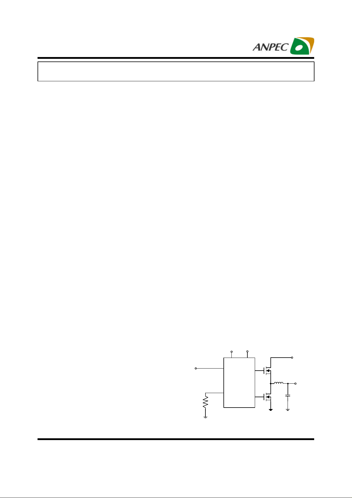
Simpilfied Application Circuit
V
+3V~25V
L
IN
V
OUT
FCCM
(Only QFN)
R
FSET
VCC=5V
APW7138
EN
Q1
Q2
www.anpec.com.tw1
APW7138
Ordering and Marking Information
APW7138
Assembly Material
Handling Code
Temperature Range
Package Code
APW7138 N :
APW7138 QA :
APW7138 QB :
Note: ANPEC lead-free products contain molding compounds/die attach materials and 100% matte tin plate termination finish; which
are fully compliant with RoHS. ANPEC lead-free products meet or exceed the lead-free requirements of IPC/JEDEC J-STD-020D for
MSL classification at lead-free peak reflow temperature. ANPEC defines “Green” to mean lead-free (RoHS compliant) and halogen
free (Br or Cl does not exceed 900ppm by weight in homogeneous material and total of Br and Cl does not exceed 1500ppm by
weight).
APW7138
XXXX
APW7138
XXXX
APW
7138
XXXX
Package Code
N : SSOP-16 QA: QFN4x4-16A QB: TQFN3x3-16
Operating Ambient Temperature Range
I : -40 to 85 oC
Handling Code
TR : Tape & Reel
Assembly Material
G : Halogen and Lead Free Device
XXXXX - Date Code
XXXXX - Date Code
XXXXX - Date Code
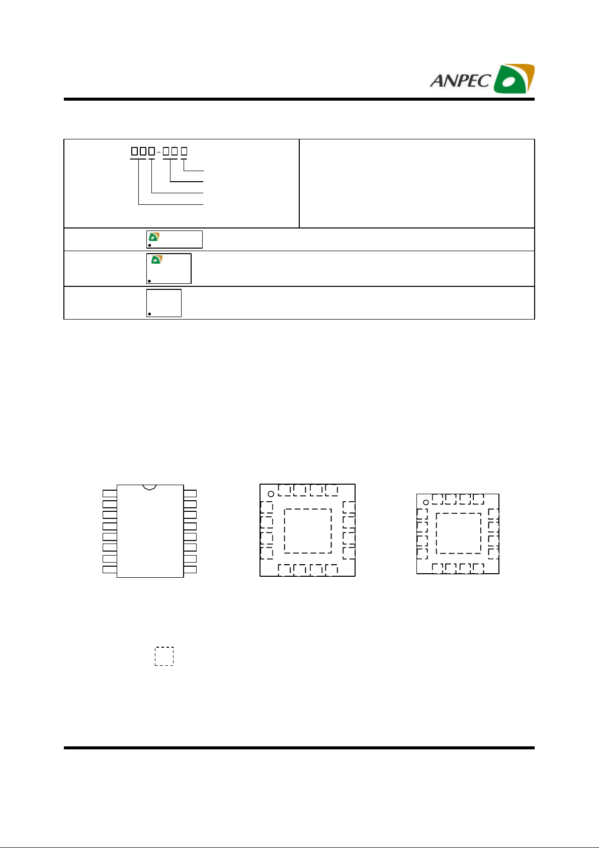
Pin Configuration
VIN
VCC
EN
NC
FB
GND
1
2
3
4
5
6
7
8
SSOP-16
(TOP VIEW)
16
UG
BOOT
15
PVCC
14
13
LG
12
PGND
ISEN
11
VO
10
9
FSET
= Thermal Pad (connected to GND plane for better heat dissipation)
PHASE
PGOOD
Copyright ANPEC Electronics Corp.
Rev. A.5 - Jul., 2010
VIN
VCC
FCCM
EN
1
2
3
4
PHASE
PGOOD
NC
UG
1516 14 13
Metal
GND Pad
(Bottem)
65 7 8
FB
FSET
QFN4x4-16A
(TOP VIEW)
BOOT
12
PVCC
11
LG
10
PGND
ISEN
9
VO
VIN
VCC
FCCM
EN
1
2
3
4
PHASE
UG
PGOOD
1516 14 13
Metal
GND Pad
(Bottem)
65 7 8
FB
NC
FSET
TQFN3x3-16
(TOP VIEW)
www.anpec.com.tw2
BOOT
12
PVCC
11
LG
PGND
10
ISEN
9
VO

APW7138
Absolute Maximum Ratings (Note 1)
Symbol Parameter Rating Unit
VCC VCC Supply Voltage (VCC to GND) -0.3 ~ 7 V
V
PVCC Supply Voltage (PVCC to GND) -0.3 ~ 7 V
PVCC
VIN Input Power Voltage (VIN to GND) -0.3 ~28 V
V
BOOT Supply Voltage (BOOT to PHASE) -0.3 ~ 7 V
BOOT
V
V
V
Note 1: Absolute Maximum Ratings are those values beyond which the life of a device may be impaired. Exposure to absolute
maximum rating conditions for extended periods may affect device reliability.
BOOT Supply Voltage (BOOT to GND) -0.3 ~ 35 V
BOOT-GND
UG Voltage (UG to PHASE)
UG-PHASE
<400ns pulse width
>400ns pulse width
LG Voltage (LG to PGND)
LG-PGND
<400ns pulse width
>400ns pulse width
PHASE Voltage (PHASE to GND)
V
PHASE
<400ns pulse width
>400ns pulse width
V
PGND to GND Voltage -0.3 ~ 0.3 V
PGND
V
ISEN Supply Voltage (ISEN to GND) -0.3 ~ 28 V
ISEN
V
PGOOD Supply Voltage (PGOOD to GND) -0.3 ~ 7 V
PGOOD
V
All Other Pins (VO, FB, EN, FCCM and FSET to GND) -0.3 ~ VCC+0.3 V
I/O
-5 ~ V
-0.3 ~ V
BOOT
BOOT
+0.3
+0.3
-5 ~ VCC+0.3
-0.3 ~ VCC+0.3
-5 ~ 35
-2 ~ 28
TJ Maximum Junction Temperature 150
T
Storage Temperature Range -65 ~ 150
STG
T
Maximum Lead Soldering Temperature, 10 Seconds 260
SDR
V
V
V
°C
°C
°C
Thermal Characteristics (Note 2)
Symbol
Thermal Resistance -Junction to Ambient
θJA
Note 2: θJA is measured with the component mounted on a high effective thermal conductivity test board in free air. The exposed pad
of package is soldered directly on the PCB.
Parameter Typical Value Unit
SSOP-16
QFN4x4-16A
TQFN3x3-16
105
40
55
°C/W
Recommended Operating Conditions
Symbol Parameter Range Unit
VCC,V
Copyright ANPEC Electronics Corp.
Rev. A.5 - Jul., 2010
V
VIN
I
OUT
OUT
TA
TJ
VCC, PVCC Supply Voltage 4.5 ~ 5.5 V
PVCC
Converter Output Voltage 0.6 ~ 3.3 V
Converter Input Voltage 3 ~ 25 V
Converter Output Current 0 ~ 25 A
Ambient Temperature -40 ~ 85
Junction Temperature -40 ~ 125
www.anpec.com.tw3
o
C
o
C
APW7138
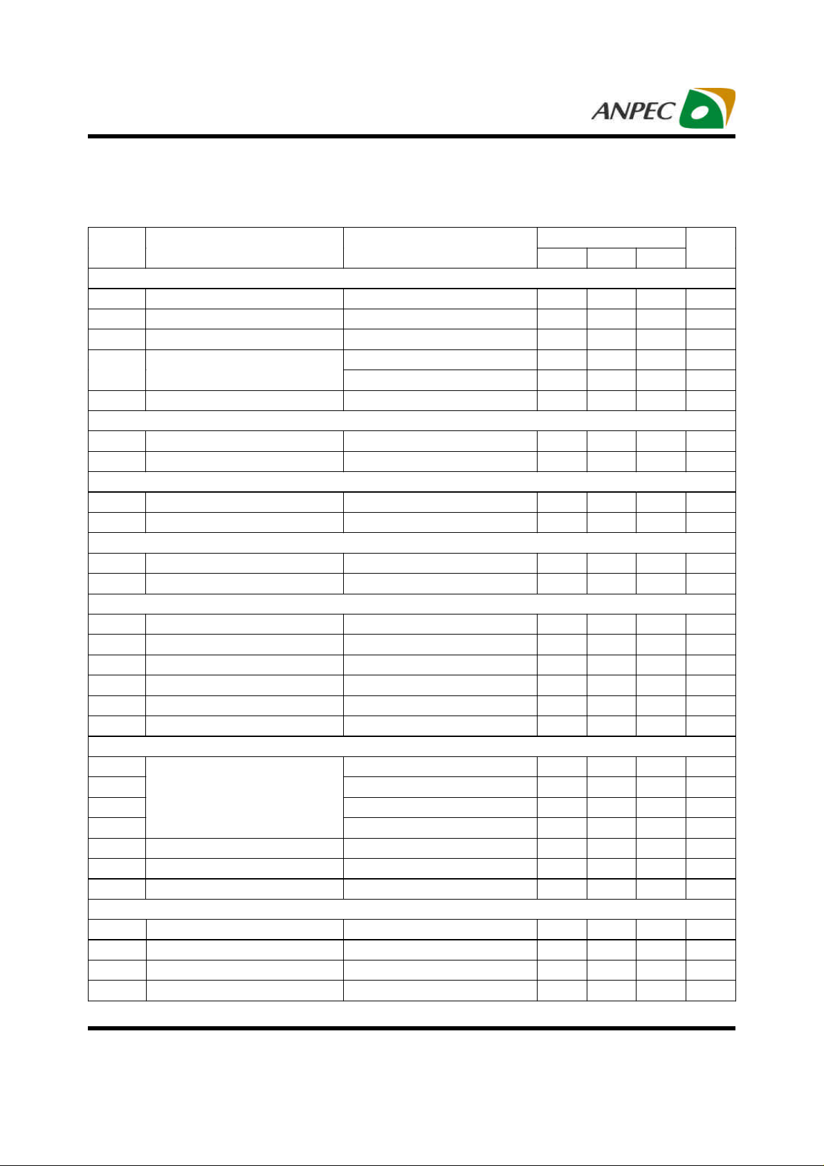
Electrical Characteristics
Refer to the typical application circuits. These specifications apply over VCC=5V, VIN=7~25V and TA= -40 ~ 85 °C, unless
otherwise specified. Typical values are at TA=25°C.
Symbol
Parameter Test Conditions
SUPPLY CURRENT
I
VCC Input Bias Current VEN=5V, VFB=0.65V, VIN=7V to 25V - 1.7 2.5 mA
VCC
VCC Shutdown Current VEN=GND, VCC=5V - 0.1 1.0
PVCC Shutdown Current VEN=GND, V
I
VIN Input Bias Current
VIN
VEN=5V, VIN=7V - 6.5 10
VEN=5V, VIN=25V - 25 35
=5V - 0.1 1.0
PVCC
VIN Shutdown Current VEN=GND, VIN=25V - 0.1 1.0
POWER-ON-RESET (POR)
V
VCC_THR
Rising VCC POR Threshold Voltage 4.1 4.2 4.3 V
VCC POR Hysteresis - 0.2 - V
VOLTAGE REGULATION
V
Reference Voltage - 0.6 - V
REF
Regulation Accuracy Over Temperature -1 - +1 %
SWITCHING FREQUENCY
FSW Frequency Range DC Output Current 200 - 600 kHz
Frequency-Set-Accuracy
R
FSET
=44.5kΩ
PWM CONVERTERS
UG Minimum-Off Time Over temperature and VCC - 550 - ns
VO Pin Input Impedance V
= 3.3V - 134 -
OUT
IFB FB Input Bias Current VFB=0.6V -0.5 - +0.5
TSS Soft-Start Time VEN High to V
Regulation
OUT
(Note3)
- 1.5 - ms
Zero-Crossing Voltage Threshold -5 0 +5 mV
On-Time Ratio of PFM to PWM - 1.5 - -
POWER GOOD
R
I
PG_SS
R
I
PG_UV
R
PG_OV
R
PG_OC
I
PGOOD
PGOOD Pull-Down Impedance
I
PGOOD Leakage Current V
=5mA Sink (Soft-Start) 75 95 125
PGOOD
=5mA Sink (Under-Voltage) 75 95 125
PGOOD
=5mA Sink (Over-Voltage) 50 63 85
PGOOD
I
=5mA Sink (Over-Current) 25 32 45
PGOOD
=5V - 0.1 1.0
PGOOD
PGOOD Maximum Sink Current - 5.0 - mA
PGOOD Soft-Start Delay VEN High to V
High 2.20 2.75 3.30 ms
PGOOD
MOSFET GATE DRIVERS
UG Pull-Up Resistance V
UG Source Current V
UG Sink Resistance V
UG Sink Current V
=5V, IUG=0.1A - 1 2
BOOT
=5V, VUG-V
BOOT
=5V, IUG=0.1A - 1 2
BOOT
=5V, VUG-V
BOOT
=2.5V - 2 - A
PHASE
=2.5V - 2 - A
PHASE
APW7138
Min. Typ. Max.
Unit
µA
µA
µA
µA
µA
270 300 330 kHz
kΩ
µA
Ω
Ω
Ω
Ω
µA
Ω
Ω
Copyright ANPEC Electronics Corp.
www.anpec.com.tw4
Rev. A.5 - Jul., 2010

APW7138
Electrical Characteristics (Cont.)
Refer to the typical application circuits. These specifications apply over VCC=5V, VIN=7~25V and TA= -40 ~ 85 °C, unless
otherwise specified. Typical values are at TA=25°C.
Symbol
Parameter Test Conditions
APW7138
Min. Typ. Max.
MOSFET GATE DRIVERS (CONT.)
LG Pull-Up Resistance V
LG Source Current V
LG Sink Resistance V
LG Sink Current V
=5V, ILG=0.1A - 1 2
PVCC
=5V, VLG-V
PVCC
=5V, ILG=0.1A - 0.6 1.2
PVCC
=5V, VLG-V
PVCC
=2.5V - 2 - A
PGND
=2.5V - 3 - A
PGND
TD Dead Time - 20 - ns
BOOTSTRAP DIODE
VF Forward Voltage V
PVCC-VBOOT-GND
=5V, IF=2mA - 0.8 - V
IR Reverse Leakage VR=25V - 0.2 -
CONTROL INPUTS
V
FCCMTHR
V
FCCMTHF
V
V
FCCM High Threshold 2.0 - - V
FCCM Low Threshold
EN High Threshold 2.0 - - V
ENR
EN Low Threshold - - 0.8 V
ENF
Only for QFN4x4-16A and
TQFN3x3-16 packages
- - 0.8 V
EN Leakage VEN=5V - 0.1 1.0
PROTECTION
IOC ISEN OCP Threshold I
ISC ISEN Short-Circuit Threshold I
Sourcing 20 26 30
SEN
Sourcing - 50 -
SEN
VUV UVP Threshold 65 70 75 %
UVP Debounce Interval - 2 -
V
OVP Rising Threshold 119 124 129 %
OVR
V
OVP Falling Threshold 99 104 109 %
OVF
OVP Debounce Interval - 2 -
T
OTP Rising Threshold
OTR
OTP Hysteresis
Note 3: Guaranteed by design.
(Note 3)
- 150 -
(Note 3)
- 25 -
Unit
Ω
Ω
µA
µA
µA
µA
µs
µs
o
C
o
C
Copyright ANPEC Electronics Corp.
www.anpec.com.tw5
Rev. A.5 - Jul., 2010
APW7138
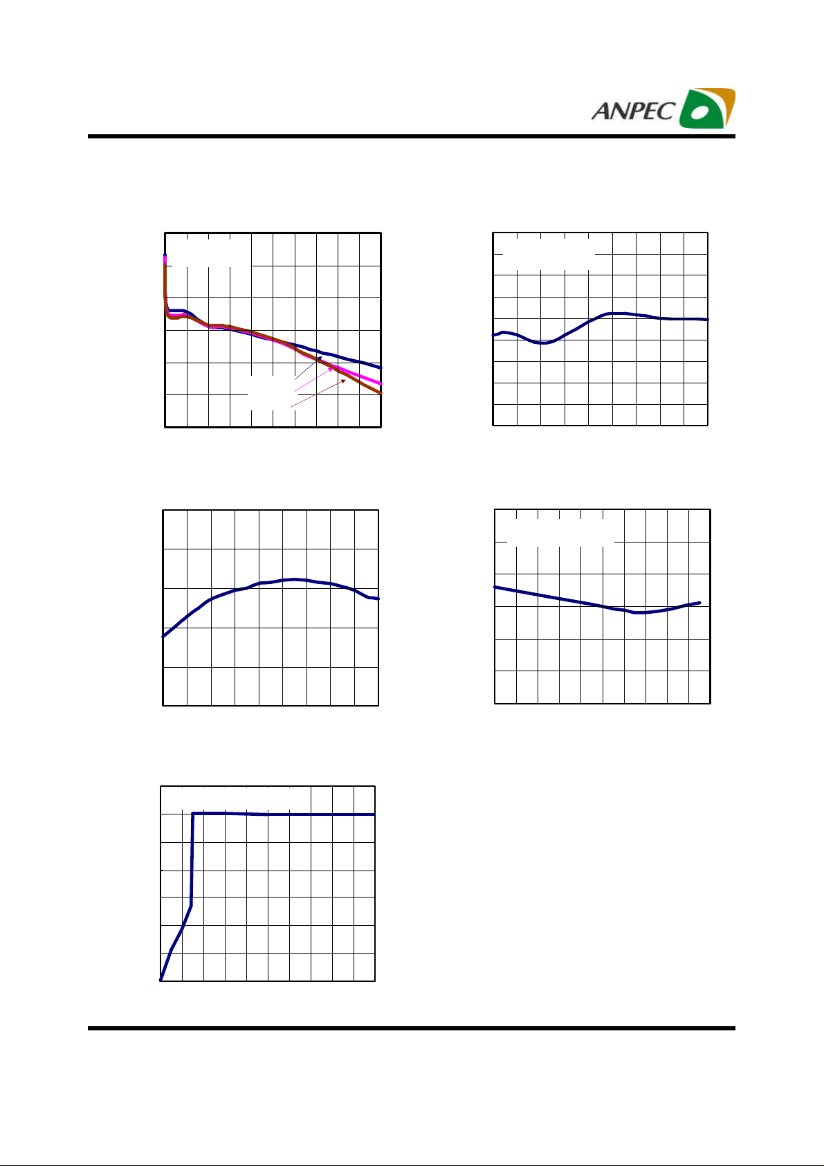
Typical Operating Characteristics
Output Voltage vs. Output Current
1.215
V
=1.2V
1.21
(V)
1.205
OUT
1.2
1.195
Output Voltage, V
1.190
1.185
OUT
V
=19V
IN1
V
=15V
IN1
V
=10V
IN1
0 1 2 3 4 5 6 7 8 9 10
Output Current, I
OUT
Reference Voltage Accuracy Over
Temperature
0.604
0.602
(V)
REF
0.6
0.598
(A)
Switching Frequency (300kHz)
345
335
325
(kHz)
SW
315
305
295
285
275
265
Switching Frequency, F
255
-40
Over Temperature
In PWM Mode
DC Output Current
-20 0 20 40
Junction Temperature, TJ (oC)
Switching Frequency vs. V
330
In PWM Mode
(kHz)
SW
320
310
300
290
DC Output Current
60 80 100 120 140
IN
0.596
Reference Voltage, V
0.594
-40 -20 0
20 40 60 80
Junction Temperature, TJ (oC)
Switching Frequency vs.
Ouput Current
350
300
(kHz)
250
SW
200
150
100
Switching Frequency, F
Copyright ANPEC Electronics Corp.
Rev. A.5 - Jul., 2010
V
=1.2V, I
OUT
50
0
0 1 2 3 4 5 6 7 8 9 10
Output Current, I
OUT
rising
OUT
(A)
100
120 140
280
Switching Frequency, F
270
5 7 9 11 13 15 17 19 21 23 25
Input Voltage, VIN (V)
www.anpec.com.tw6
APW7138
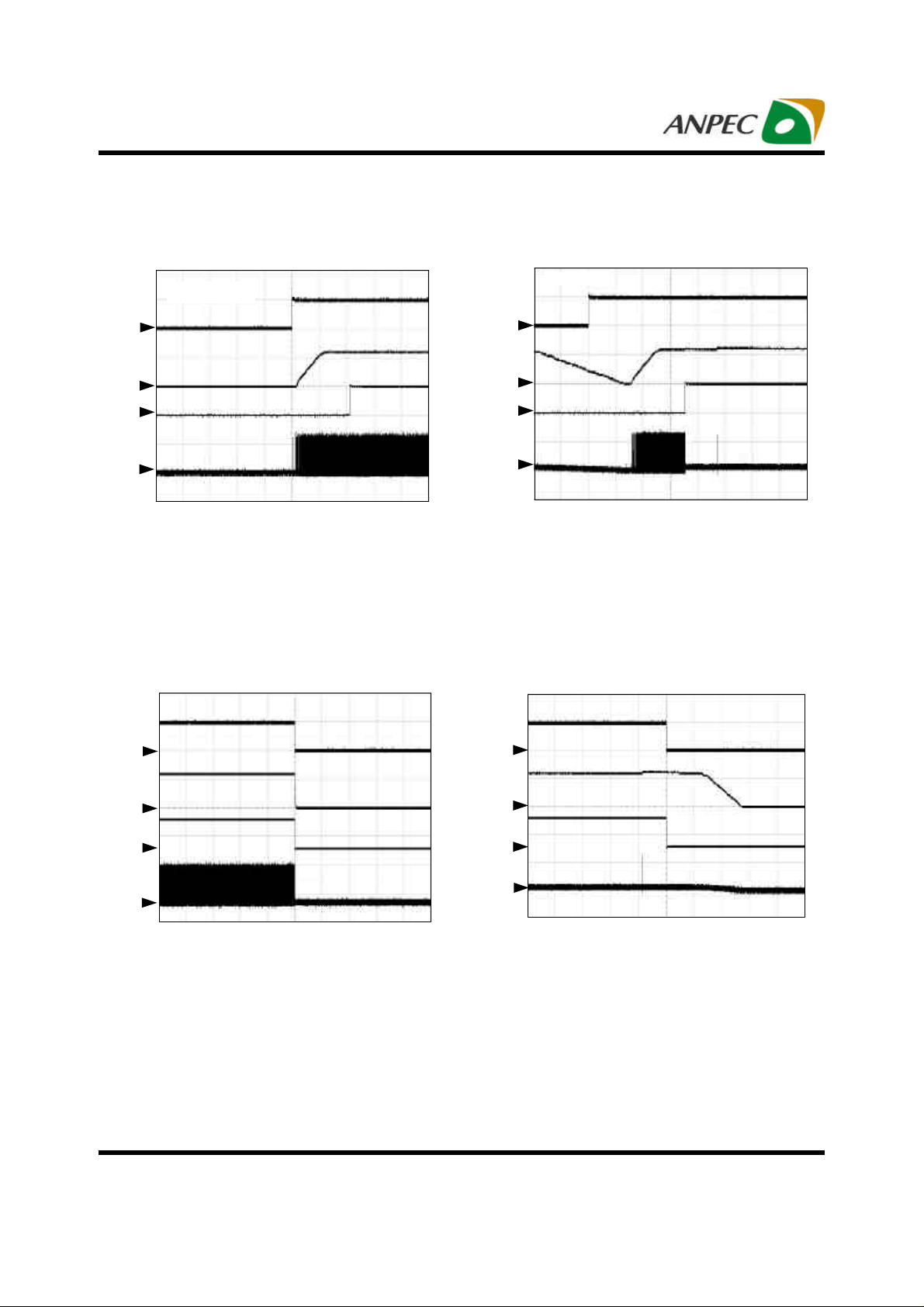
Operating Waveforms
Enable at Zero Initial Voltage of V
I
=5A
OUT
1
2
3
4
CH1: VEN (5V/div)
CH2: V
CH3: V
CH4: V
Time: 2ms/div
OUT
PGOOD
PHASE
(1V/div)
(5V/div)
(10V/div)
Shutdown at I
OUT
=5A
OUT
Enable Before End of Soft-Stop
No Load
1
2
3
4
CH1: VEN (5V/div)
CH2: V
CH3: V
CH4: V
Time: 2ms/div
OUT
PGOOD
PHASE
(1V/div)
(5V/div)
(10V/div)
Shutdown with Soft-Stop at No Load
1
2
3
4
CH1: VEN (5V/div)
CH2: V
CH3: V
CH4: V
Time: 5ms/div
OUT
PGOOD
PHASE
(1V/div)
(5V/div)
(10V/div)
Copyright ANPEC Electronics Corp.
Rev. A.5 - Jul., 2010
1
2
3
4
CH1: VEN (5V/div)
CH2: V
CH3: V
CH4: V
Time: 5ms/div
OUT
PGOOD
PHASE
(1V/div)
(5V/div)
(10V/div)
www.anpec.com.tw7
APW7138
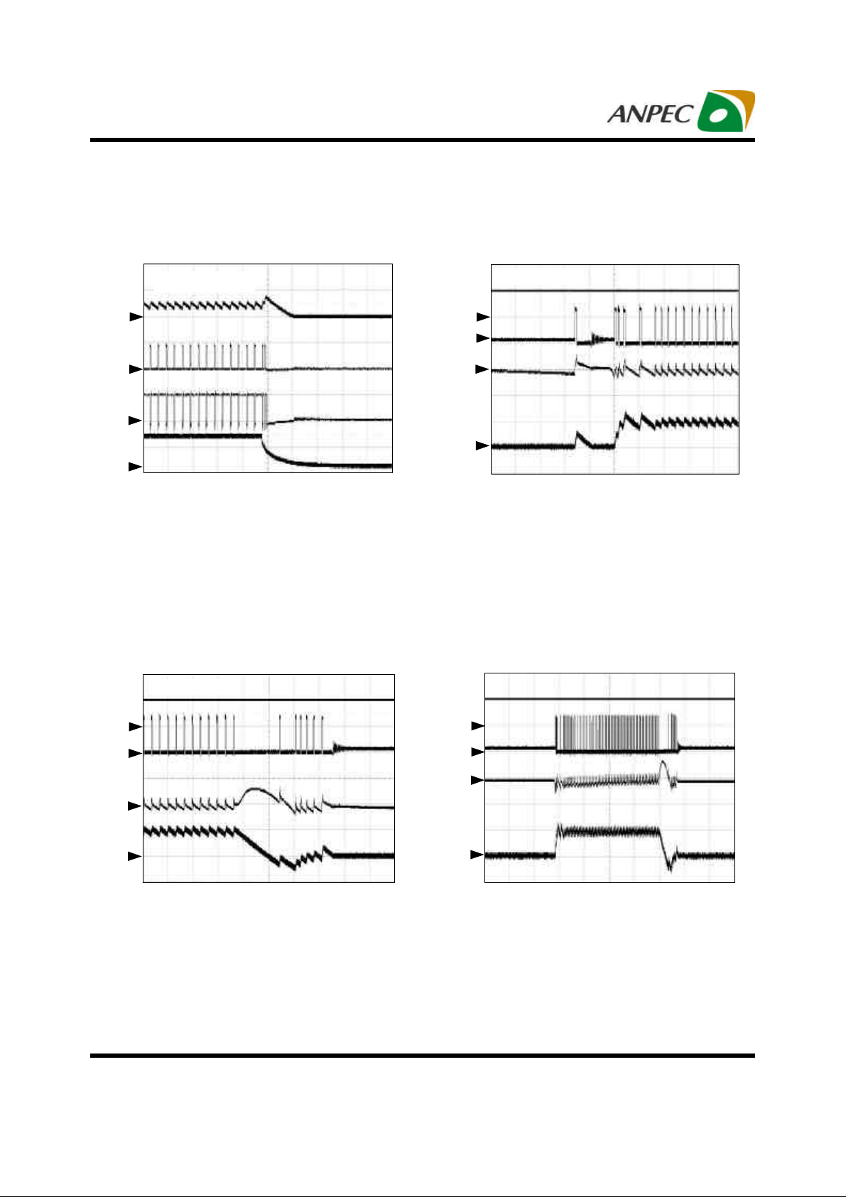
Operating Waveforms (Cont.)
Under-Voltage Protection
Short Circuit Test
1
2
3
4
CH1: IL (5A/div)
CH2: V
CH3: VLG (5V/div)
CH4: V
Time: 10µs/div
(20V/div)
UG
(1V/div)
OUT
Mode Transient From PWM to PFM
Mode Transient From PFM to PWM
I
=0.1A to 5A
OUT
1
2
3
4
CH1: V
CH2: V
CH3: V
CH4: IL (5A/div)
(5V/div)
PGOOD
(10V/div)
PHASE
(AC, 100mV/div)
OUT
Time: 10µs/div
Load Transient
0A->5A->0A
I
=5A to 0.1A
OUT
1
2
3
4
CH1: V
CH2: V
CH3: V
CH4: IL (5A/div)
(5V/div)
PGOOD
(10V/div)
PHASE
(AC, 100mV/div)
OUT
Time: 10µs/div
Copyright ANPEC Electronics Corp.
Rev. A.5 - Jul., 2010
I
OUT1
1
2
3
4
CH1: V
CH2: V
CH3: V
CH4: IL (5A/div)
Time: 50µs/div
rise/fall time=1us
(5V/div)
PGOOD
(10V/div)
PHASE
(AC, 100mV/div)
OUT
www.anpec.com.tw8
APW7138
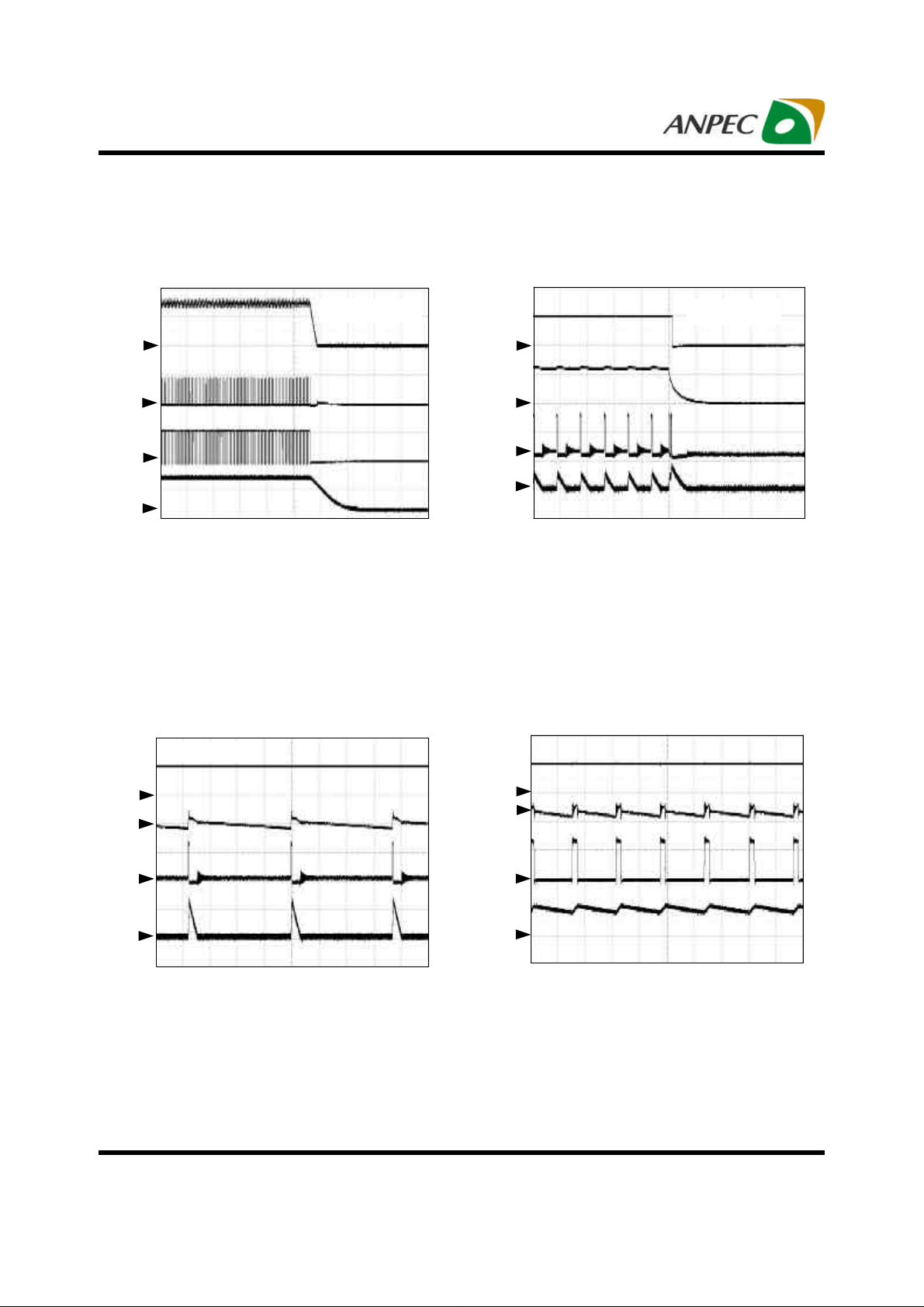
Operating Waveforms (Cont.)
Over-Current Protection
1
2
3
4
CH1: IL (5A/div)
CH2: VUG (20V/div)
CH3: VLG (5V/div)
CH4: V
Time: 50µs/div
OUT
(1V/div)
Operating at Light Load of 100mA
I
rises slowly
OUT
1
2
3
4
CH1: V
CH2: V
CH3: V
CH4: IL (5A/div)
Time: 20µs/div
Short Circuit Test
In PFM Mode
(5V/div)
PGOOD
(1V/div)
OUT
(10V/div)
PHASE
Operating at Heavy Load of 5A
In PFM Mode
1
2
3
4
CH1: V
CH2: V
CH3: V
CH4: IL (2A/div)
(5V/div)
PGOOD
(AC, 100mV/div)
OUT1
(10V/div)
PHASE
Time: 20us/div
Copyright ANPEC Electronics Corp.
Rev. A.5 - Jul., 2010
1
2
3
4
CH1: V
CH2: V
CH3: V
CH4: IL (5A/div)
Time: 2µs/div
(5V/div)
PGOOD
(AC, 100mV/div)
OUT1
(10V/div)
PHASE
www.anpec.com.tw9
 Loading...