Anpec APW7136ACITRG, APW7136BCITRG, APW7136CCITRG Schematic [ru]
APW7136A/B/C
1MHz, High-Efficiency, Step-Up Converter for 2 to 8 White LEDs
Features
• Wide Input Voltage from 2.7V to 6V
• 0.25V Reference Voltage
• Fixed 1MHz Switching Frequency
• High Efficiency up to 87%
• 100Hz to 100kHz PWM Brightness Control
Frequency
• Open-LED Protection
• Under-Voltage Lockout Protection
• Over-Temperature Protection
• <1µA Quiescent Current Dduring Shutdown
• SOT-23-6 Packages
• Lead Free and Green Devices Available
(RoHS Compliant)
Applications
General Description
The APW7136A/B/C is a current-mode and fixed frequency
boost converter with an integrated N-FET to drive up to 8
white LEDs in series.
The series connection allows the LED current to be identical for uniform brightness. Its low on-resistance of NFET and feedback voltage reduce power loss and achieve
high efficiency. Fast 1MHz current-mode PWM operation
is available for input and output capacitors and a s mall
inductor while minimizing ripple on the input supply. The
OVP pin monitors the output voltage and stops switching
if exceeds the over-voltage threshold. An internal softstart circuit eliminates the inrush current during s tart-up.
The APW7136A/B/C also integrates under-voltage
lockout, over-temperature protection, and c urrent-limit
circuits. The APW7136/A/B/C is available in a SOT-23-6
packages.
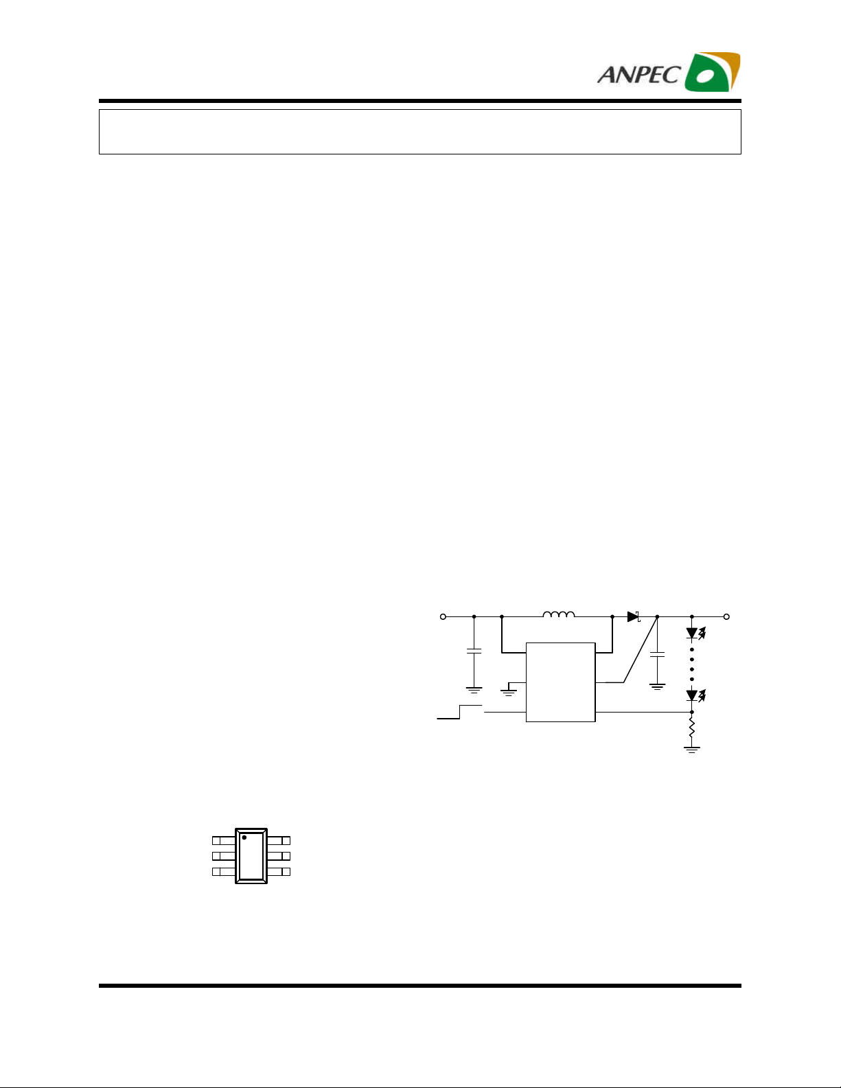
Simplified Application Circuit
• White LED Display Backlighting
• Cell Phone and Smart Phone
• PDA, PMP, MP3
• Digital Camera
V
IN
C1
4.7µF
OFF ON
6
2
4
VIN
GND
EN
L1
22µH
LX
OVP
FB
1
5
3
C2
1µF
V
OUT
Up to 8
WLEDs
R1
12Ω
Pin Configuration
SOT-23-6 Top View
LX 1
GND 2
FB 3
ANPEC reserves the right to make changes to improve reliability or manufacturability without notice, and
advise customers to obtain the latest version of relevant information to verify before placing orders.
Copyright ANPEC Electronics Corp.
Rev. A.4 - Dec., 2010
6 VIN
5 OVP
4 EN
www.anpec.com.tw1
APW7136A/B/C
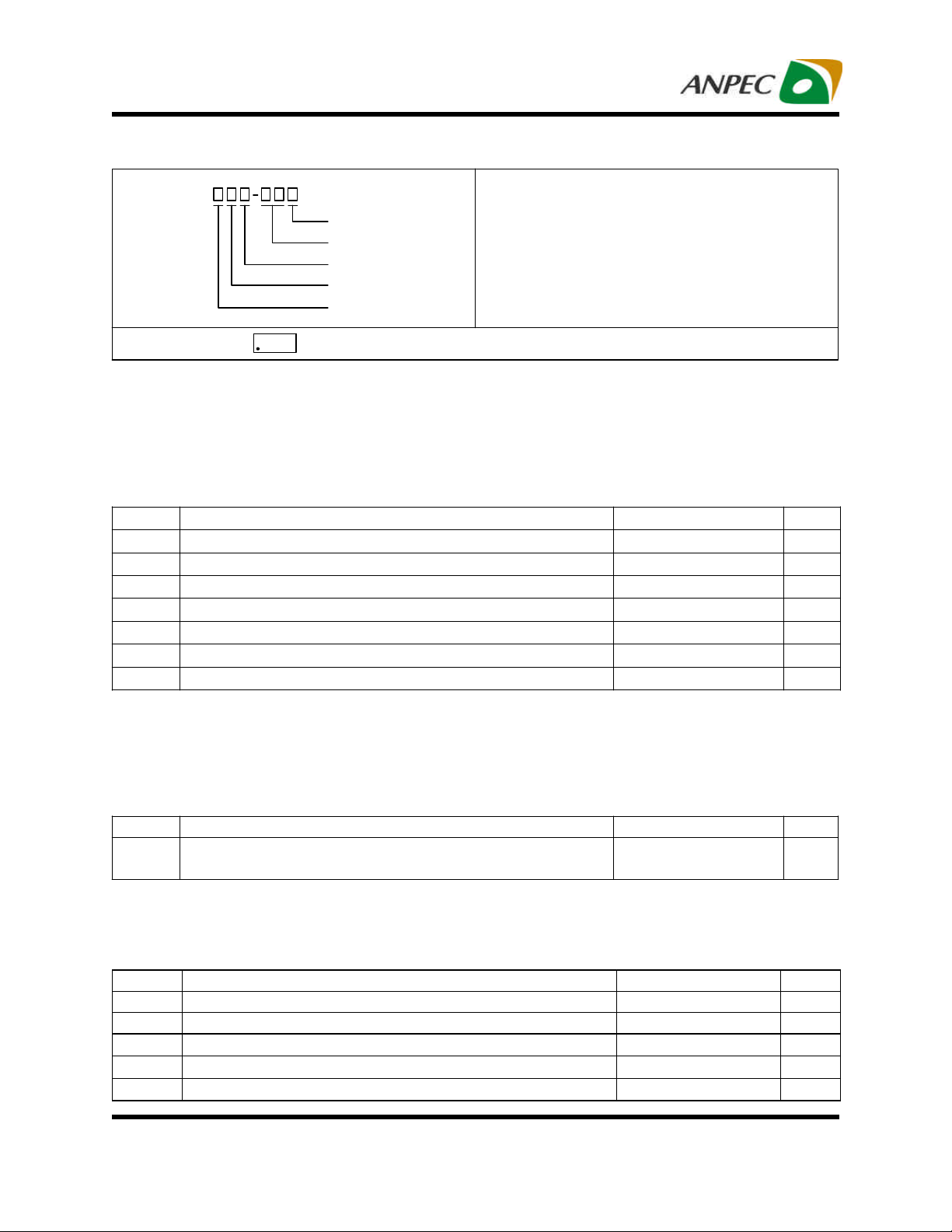
Ordering and Marking Information
APW7136
Assembly Material
Handling Code
Temperature Range
Package Code
OVP Voltage Code
APW7136YCI :
CFYX
Note: ANPEC lead-free products contain molding compounds/die attach materials and 100% matte tin plate termination finish; which
are fully compliant with RoHS. ANPEC lead-free products meet or exceed the lead-free requirements of IPC/JEDEC J-STD-020D for
MSL classification at lead-free peak reflow temperature. ANPEC defines “Green” to mean lead-free (RoHS compliant) and halogen
free (Br or Cl does not exceed 900ppm by weight in homogeneous material and total of Br and Cl does not exceed 1500ppm by
weight).
Absolute Maximum Ratings (Note 1)
Symbol
VIN VIN Supply Voltage (VIN to GND) -0.3 ~ 8 V
FB, EN to GND Voltage -0.3 ~ VIN V
VLX LX to GND Voltage -0.3 ~ 38 V
V
OVP to GND Voltage -0.3 ~ 38 V
OVP
TJ Maximum Junction Temperature 150
T
Storage Temperature Range -65 ~ 150
STG
T
Maximum Lead Soldering Temperature, 10 Seconds 260
SDR
Note 1: Stresses beyond those listed under “Absolute Maximum Ratings” may cause permanent damage to the device. These are
stress ratings only and functional operation of the device at these or any other conditions beyond those indicated in the operational
sections of the specifications is not implied. Exposure to absolute maximum rating conditions for extended periods may affect device
reliability.
Parameter Rating Unit
OVP Voltage Code
A: 20V B: 28V C: 35V
Package Code
C : SOT-23-6
Operating Ambient Temperature Range
I : -40 to 85oC
Handling Code
TR : Tape & Reel
Assembly Material
G : Halogen and Lead Free Device
Y - OVP Voltage Code
X - Date Code
o
C
o
C
o
C
Thermal Characteristics
Symbol
θJA
Note 2: θJA is measured with the component mounted on a high effective thermal conductivity test board in free air. The exposed pad
Junction to Ambient Thermal Resistance
of package is soldered directly on the PCB.
Parameter Rating Unit
(Note 2)
SOT-23-6
250
°C/W
Recommended Operating Conditions (Note 3)
Symbol
VIN VIN Input Voltage 2.7~ 6 V
V
Converter Output Voltage Up to 32 V
OUT
CIN Input Capacitor 4.7 or higher
C
Output Capacitor 0.68 or higher
OUT
L1 Inductor 6.8 to 47
Copyright ANPEC Electronics C orp.
Rev. A.4 - Dec., 2010
Parameter Range Unit
µF
µF
µH
www.anpec.com.tw2
APW7136A/B/C
Recommended Operating Conditions (Note 3) (Cont.)
Symbol
TA Ambient Temperature -40 to 85 °C
TJ Junction Temperature -40 to 125 °C
Note 3: Refer to the application circuit for further information.
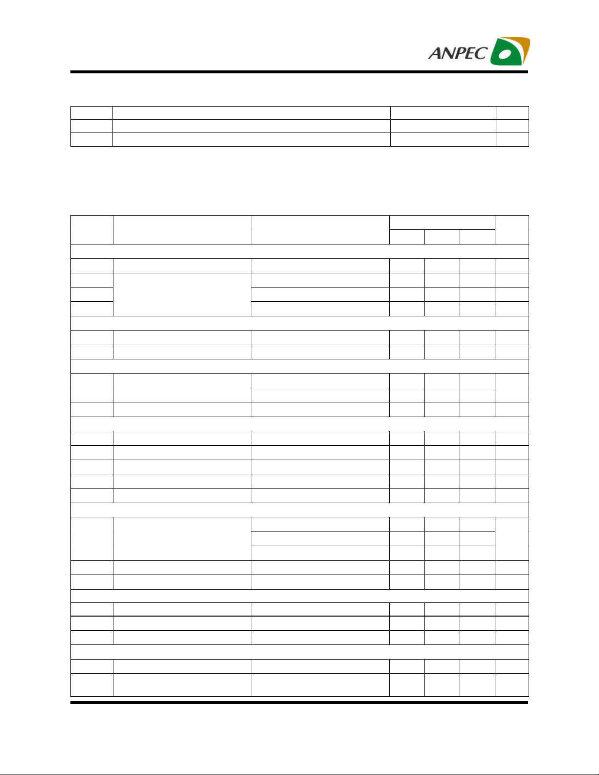
Electrical Characteristics
(Refer to Figure 1 in the “Typical Application Circuits.” These specifications apply over VIN = 3.6V, TA = -40°C to 85°C,
unless otherwise noted. Typical values are at TA = 25°C.)
Parameter Range Unit
Symbol
Parameter Test Conditions
APW7136A/B/C
Min. Typ. Max.
SUPPLY VOLTAGE AND CURRENT
VIN Input Voltage Range TA = -40 ~ 85°C, TJ = -40 ~ 125°C 2.7 - 6 V
I
V
DD1
I
DD2
Input DC Bias Current
FB = GND, switching - 1 2 mA
ISD
= 1.3V, no switching 70 100 130 µA
FB
EN = GND - - 1 µA
UNDER-VOLTAGE LOCKOUT
UVLO Threshold Voltage VIN Rising 2.0 2.2 2.4 V
UVLO Hysteresis Voltage 50 100 150 mV
REFERENCE AND OUTPUT VOLTAGES
V
Regulated Feedback Voltage
REF
TA = 25°C 237 250 263
TA = -40 ~ 85°C (TJ = -40 ~ 125°C) 230 - 270
IFB FB Input Current -50 - 50 nA
INTERNAL POWER SWITCH
FSW Switching Frequency FB=GND 0.8 1.0 1.2 MHz
RON Power Switch On Resistance - 0.6 -
I
Power Switch Current-Limit 0.7 0.9 1.2 A
LIM
LX Leakage Current VEN=0V, VLX=0V or 5V, VIN = 5V -1 - 1 µA
D
LX Maximum Duty Cycle 92 95 98 %
MAX
OUTPUT OVER-VOLTAGE PROTECTION
APW7136A - 20 -
V
Over-Voltage Threshold
OVP
APW7136B - 28 -
APW7136C - 35 OVP Hysteresis - 3 - V
OVP Leakage Current V
=30V, EN=VIN - - 50 µA
OVP
ENABLE AND SHUTDOWN
V
EN Voltage Threshold VEN Rising 0.4 0.7 1 V
TEN
EN Voltage Hysteresis - 0.1 - V
I
EN Leakage Current VEN= 0~5V, VIN = 5V -1 - 1 µA
LEN
OVER-TEMPERATURE PROTECTION
T
Over-Temperature Protection TJ Rising - 150 - °C
OTP
Over-Temperature Protection
Hysteresis
- 40 - °C
Copyright ANPEC Electronics C orp.
www.anpec.com.tw3
Rev. A.4 - Dec., 2010
Unit
mV
Ω
V
APW7136A/B/C
≅
≅
≅
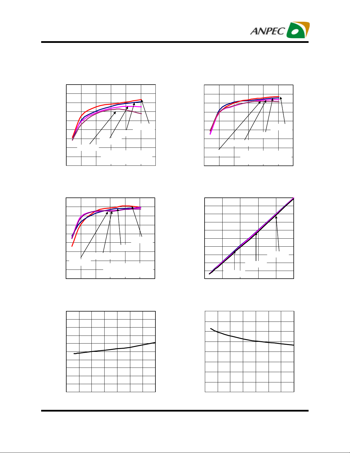
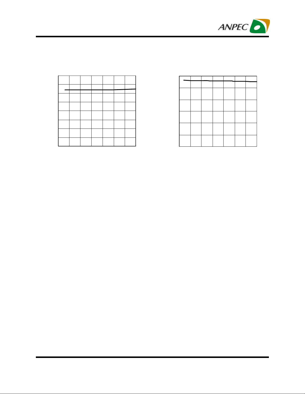
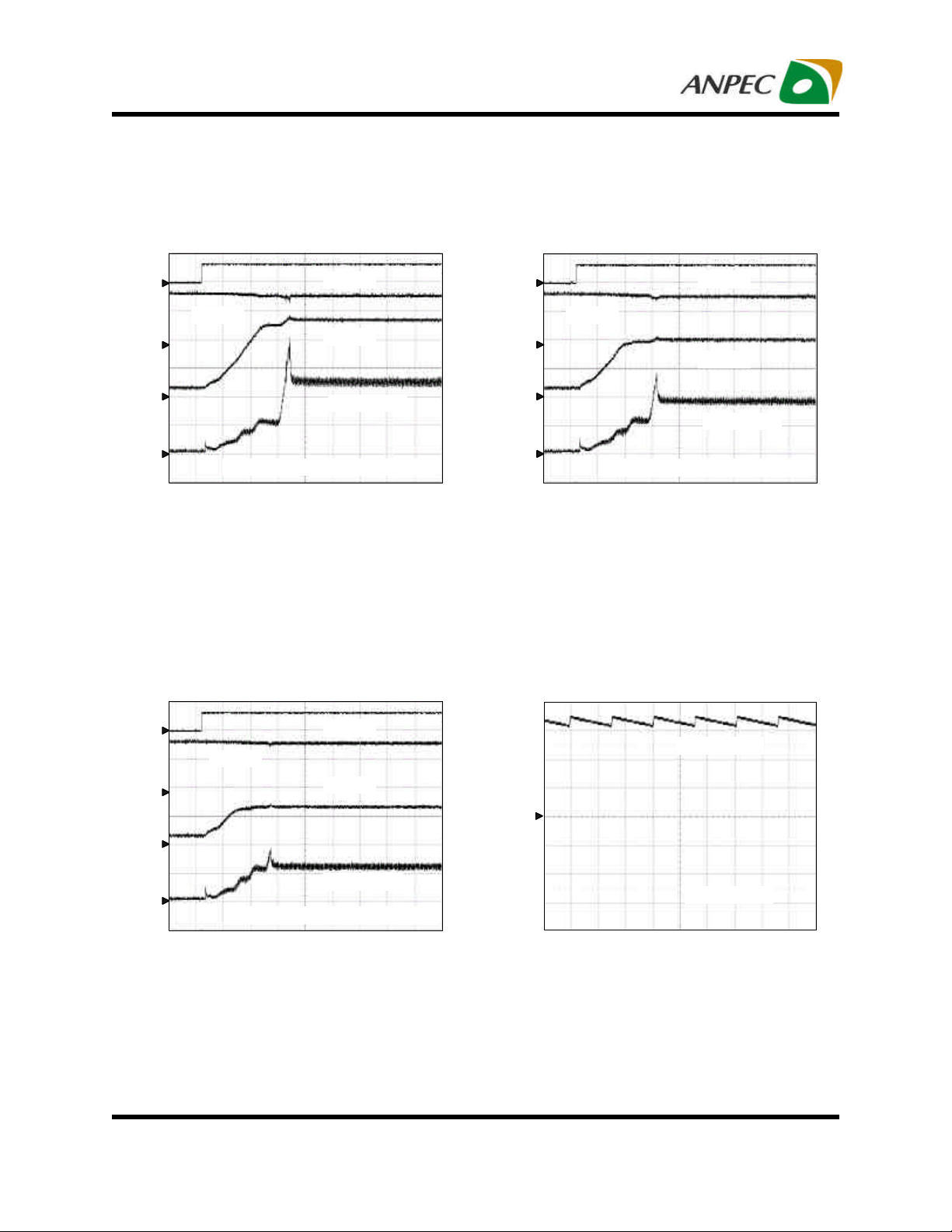
Typical Operating Characteristics
(Refer to Figure 1 in the section “Typical Application Circuits,” VIN=3.6V, TA=25oC, 8WLEDs unless otherwise specified.)
Efficiency vs. WLED Current Efficiency vs. WLED Current
95
90
85
80
75
70
Efficiency (η)
65
60
VIN=3.3V
55
VIN=4.2V
VIN=3.6V
8 WLEDs 25.6V@20mA
50
0 5 10 15 20 25 30
WLED Current, I
LED
(mA)
η=P
VIN=5V
OUT/PIN
95
90
85
80
75
70
Efficiency (η)
65
VIN=3.6V
VIN=4.2V
60
55
VIN=3.3V
6 WLEDs 19.3V@20mA
50
0 5 10 15 20 25 30
WLED Current, I
LED
(mA)
η=P
VIN=5V
OUT/PIN
Efficiency vs. WLED Current
95
90
85
80
75
70
Efficiency (η)
65
60
VIN=3.3V
VIN=3.6V
55
VIN=4.2V
4 WLEDs 13V@20mA
50
0 5 10 15 20 25 30
Supply Voltage, V
IN
WLED Current vs. Supply Voltage
21.0
20.8
20.6
20.4
(mA)
LED
20.2
20.0
19.8
19.6
WLED Current, I
19.4
19.2
19.0
2.5 3 3.5 4 4.5 5 5.5 6
Supply Voltage, V
Copyright ANPEC Electronics C orp.
Rev. A.4 - Dec., 2010
IN
(V)
(V)
η=P
VIN=5V
OUT/PIN
WLED Current vs. PWM Duty Cycle
20
18
16
14
(mA)
LED
12
10
8
6
WLED Current, I
4
2
100Hz
1kHz
100KHz
0
0 20 40 60 80 100
PWM Duty Cycle (%)
Switch ON Resistance vs. Supply Voltage
0.8
0.7
(Ω)
ON
0.6
0.5
0.4
0.3
0.2
0.1
Switch ON Resistance, R
0
2.5 3 3.5 4 4.5 5 5.5 6
Supply Voltage, V
(V)
IN
www.anpec.com.tw4
APW7136A/B/C
Typical Operating Characteristics
(Refer to Figure 1 in the section “Typical Application Circuits,” VIN=3.6V, TA=25oC, 8WLEDs unless otherwise specified.)
Switching Frequency vs. Supply Voltage Maximum Duty Cycle vs. Supply Voltage
1.2
1.1
(MHz)
1
SW
0.9
100
90
(%)
MAX
80
0.8
0.7
0.6
0.5
Switching Frequency, F
0.4
2.5 3 3.5 4 4.5 5 5.5 6
Supply Voltage, V
(V)
IN
70
60
50
Maximum Duty Cycle, D
40
2.5 3 3.5 4 4.5 5 5.5 6
Supply Voltage, V
IN
(V)
Copyright ANPEC Electronics C orp.
Rev. A.4 - Dec., 2010
www.anpec.com.tw5
APW7136A/B/C
Operating Waveforms
(Refer to the application circuit in the section “Typical Application Circuits”, VIN=3.6V, TA=25oC, 8WLEDs unless otherwise specified.)
1
V
IN
2
3
4
CH1: VEN, 2V/Div, DC
CH2: VIN, 2V/Div, DC
CH3: V
, 10V/Div, DC
OUT
CH4: IL, 0.1A/Div, DC
Time: 1ms/Div
Start-up
V
EN
V
OUT
IIN, 0.1A/Div
8WLEDs, L=22µH, VIN=3.6V, I
Start-up
LED
=20mA
1
V
IN
2
3
4
CH1: VEN, 2V/Div, DC
CH2: VIN, 2V/Div, DC
CH3: V
, 10V/Div, DC
OUT
CH4: IL, 0.1A/Div, DC
Time: 1ms/Div
Open-LED Protection
Start-up
V
EN
V
OUT
IIN, 0.1A/Div
6WLEDs, L=22µH, VIN=3.6V, I
LED
=20mA
1
V
IN
2
3
4
4WLEDs, L=22µH, VIN=3.6V, I
V
V
IIN, 0.1A/Div
CH1: VEN, 2V/Div, DC
CH2: VIN, 2V/Div, DC
CH3: V
, 10V/Div, DC
OUT
CH4: IL, 0.1A/Div, DC
Time: 1ms/Div
Copyright ANPEC Electronics C orp.
Rev. A.4 - Dec., 2010
EN
OUT
LED
=20mA
1
CH1: V
Time: 20ms/Div
, 10V/Div, DC
OUT
V
,10V/Div
OUT
APW7136C
www.anpec.com.tw6
 Loading...