

APW7079
Low-Supply-Current Synchronous Step-up DC-DC Converter
Features
• 0.9V Typical Start-up Input Voltage
• 11µA Typical No Load Quiescent Current
• PFM Operation
• High Efficiency up to 92%
• Fixed 1.8V, 2.6V, 2.8V, 3V, 3.3V, 3.8V, 4.5V or 5V
Output Voltage
• 600mA Internal Switch Current
• Internal Synchronous Rectifier
• SOT-89 Package
• Lead Free and Green Devices Available
(RoHS Compliant)
Applications
• Toy
• Wireless Mouse
• Portable Instrument
Pin Configuration
SOT-89
General Description
The APW7079 is a compact, PFM mode, and step-up
DC-DC converter with low quiescent current. The internal synchronous rectifier reduces cost and PCB space
by eliminating the need for an external Schottky diode.
Low on-resistance of the internal switches improves the
efficiency up to 92%. The start-up voltage is guaranteed
below 1V. After start-up, the device can operate with input
voltage down to 0.7V. The APW7079 is suitable for portable battery-powered applications. Consuming only 11µA
quiescent current and an optimized control scheme allows the device to operate at very high efficiency over the
entire load current range.
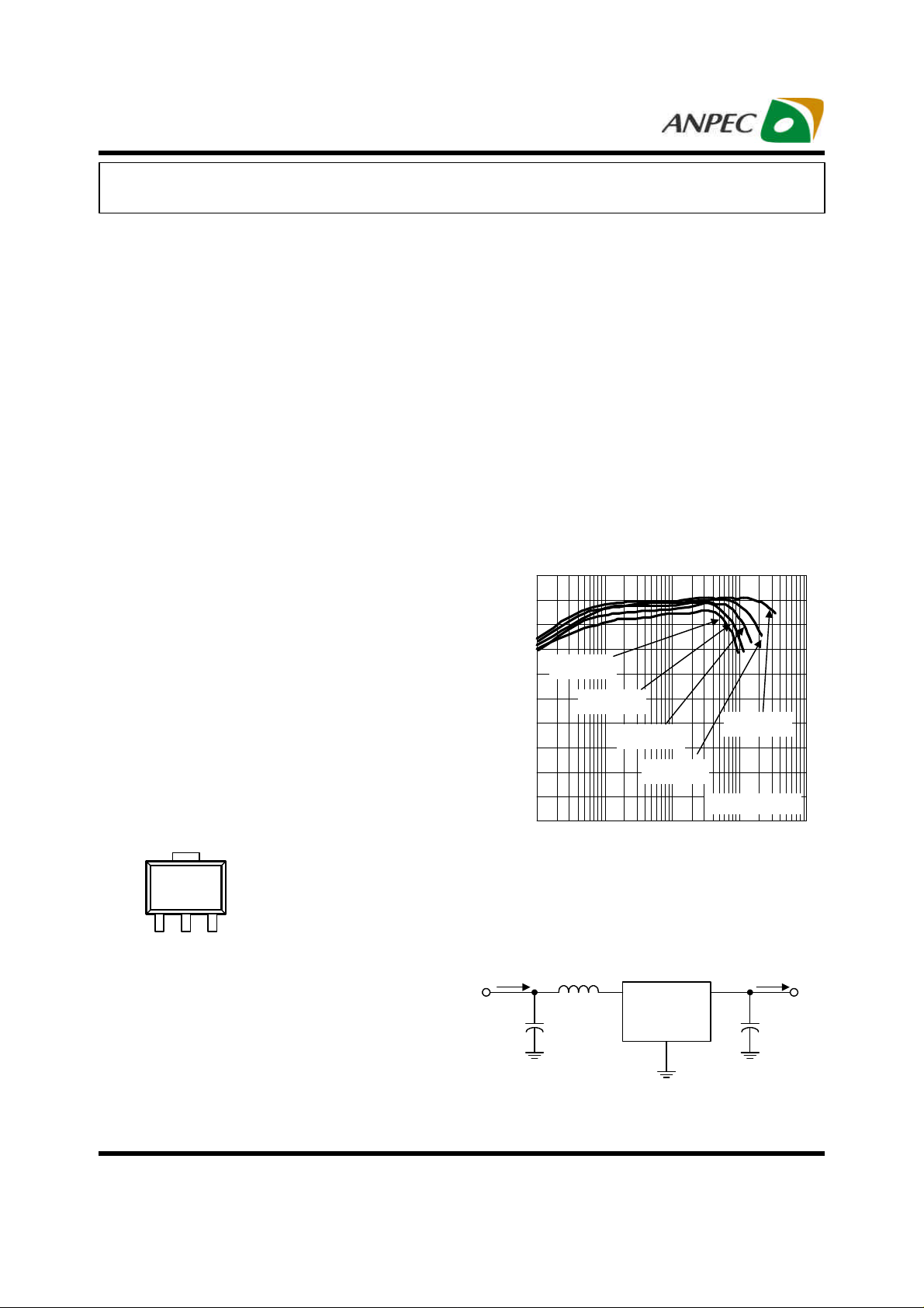
Efficiency vs. Output Current
100
90
80
70
60
50
40
Efficiency (%)
30
20
10
VIN=0.9V
VIN=1.0V
VIN=1.2V
VIN=1.5V
0
0.1 1 10 100 1000
VIN=2.4V
APW7079-30
Output Current, I
OUT
(mA)
Simplified Application Circuit
2
LX 3
(TAB)
GND 1
VOUT
Top View
ANPEC reserves the right to make changes to improve reliability or manufacturability without notice, and
advise customers to obtain the latest version of relevant information to verify before placing orders.
Copyright ANPEC Electronics Corp.
Rev. A.4 - Jun., 2009
V
I
IN
IN
L1
22µH
C1
22µF
APW7079
LX VOUT
GND
V
I
OUT
OUT
C2
47µF
www.anpec.com.tw1
APW7079
79
Ordering and Marking Information
Package Code
APW7079
Assembly Material
Handling Code
Temperature Range
Package Code
Voltage Code
APW7079-18D: XXXXX - Date Code, 18: 1.8V
APW7079-28D: XXXXX - Date Code, 28: 2.8V
APW7079-33D: XXXXX - Date Code, 33: 3.3V
APW7079-45D: XXXXX - Date Code, 45: 4.5V
APW7079
XXXXX18
APW7079
XXXXX28
APW7079
XXXXX33
APW7079
XXXXX45
Note: ANPEC lead-free products contain molding compounds/die attach materials and 100% matte tin plate termination finish; which
are fully compliant with RoHS. ANPEC lead-free products meet or exceed the lead-free requirements of IPC/JEDEC J-STD-020C for
MSL classification at lead-free peak reflow temperature. ANPEC defines “Green” to mean lead-free (RoHS c ompliant) and halogen
free (Br or Cl does not exceed 900ppm by weight in homogeneous material and total of Br and Cl does not exceed 1500ppm by
weight).
D : SOT-89
Operating Ambient Temperature Range
I : -40 to 85oC
Handling Code
TR : Tape & Reel
Assembly Material
G : Halogen and Lead Free Device
Voltage Code
18: 1.8V 26: 2.6V 28: 2.8V 30: 3.0V
33: 3.3V 38: 3.8V 45: 4.5V 50: 5.0V
APW7079-26D: XXXXX - Date Code, 26: 2.6V
APW7079-30D: XXXXX - Date Code, 30: 3.0V
APW7079-33D: XXXXX - Date Code, 38: 3.8V
APW7079-50D: XXXXX - Date Code, 50: 5.0V
APW7079
XXXXX26
APW7079
XXXXX30
APW7079
XXXXX38
APW7079
XXXXX50
Absolute Maximum Ratings (Note 1)
Symbol Parameter Rating Unit
V
OUT
V
LX
T
STG
T
SDR
Note 1: Absolute Maximum Ratings are those values beyond which the life of a device may be impaired. Exposure to absolute
Output Voltage (VOUT to GND) -0.3 ~ 6 V
LX to GND Voltage -0.3 ~ V
Storage Temperature -65 ~ 150
Maximum Lead Soldering Temperature, 10 Seconds 260
+1 V
OUT
°C
°C
maximum rating conditions for extended periods may affect device reliability.
Thermal Characteristics
Symbol Parameter Typical Value Unit
θJA
Note 2: θJA is measured with the component mounted on a high effective thermal conductivity test board in free air.
Thermal Resistance -Junction to Ambient
SOT-89
(Note 2)
180
o
C/W
Recommended Operating Conditions (Note 3, 4)
Symbol Parameter Range Unit
V
Output Voltage (VOUT to GND) 0.7 ~ 5.5 V
OUT
VIN Converter Supply Voltage 0.3 ~ V
VLX LX to GND Voltage -0.3 ~ V
I
Converter Output Current 0 ~ 0.9 x I
OUT
TA Ambient Temperature -40 ~ 85 °C
TJ Junction Temperature -40 ~ 125 °C
Note 3: Refer to the typical application circuit
Note 4: Refer to “Application Information” for detail value.
Copyright ANPEC Electronics Corp.
Rev. A.4 - Jun., 2009
+1 V
OUT
+0.3 V
OUT
A
OUT(MAX)
www.anpec.com.tw2
APW7079
Electrical Characteristics
Refer to Typical Application Circuits. VIN=1.5V, R
Symbol
Parameter Test Conditions
VIN Converter Supply Voltage 0.7 - 5.5 V
Start-up Voltage
V
Output Voltage
OUT
IDD Supply Current
T
OFF(MIN)
T
ON(MAX)
Main Switch Min. Off-time 0.6 0.9 1.2
Main Switch Max. On-time 3 4 5
Main Switch Max. Duty 75 - 85
R
Main Switch on Resistance ILX=100mA
N-FET
R
P-FET
I
Synchronous Switch on
Resistance
Main Switch Current Limit 500 600 700 mA
LIM
Main Switch Leakage Current - - 1
Synchronous Switch Leakage
Current
Over-Temperature Shutdown - 150 - °C
Over-Temperature Hysteresis - 40 - °C
= ∞, and TA= -40 ~ 85oC, unless otherwise noted. Typical values are at TA=25oC.
LOAD
APW7079
Min. Typ. Max.
R
=3kΩ
LOAD
APW7079-18 1.764
APW7079-26 2.548
APW7079-28 2.744
- 0.9 1 V
1.8 1.836
2.6 2.652
2.8 2.856
APW7079-30 2.94 3.0 3.06
APW7079-33 3.234
APW7079-38 3.724
3.3 3.366
3.8 3.876
APW7079-45 4.41 4.5 4.59
APW7079-50 4.9 5.0 5.1
V
= V
OUT
Measured at V
(Typ.)+0.5V
OUT
OUT
7 11 15
No Inductor Connected
APW7079-18 - 0.5 APW7079-26 - 0.4 APW7079-28 - 0.4 APW7079-30 - 0.4 APW7079-33 - 0.4 APW7079-38 - 0.4 APW7079-45 - 0.3 APW7079-50 - 0.3 APW7079-18 - 1 APW7079-26 - 0.8 APW7079-28 - 0.8 -
ILX=100mA
APW7079-30 - 0.7 APW7079-33 - 0.6 APW7079-38 - 0.5 APW7079-45 - 0.4 APW7079-50 - 0.4 -
- - 1
Unit
V
µA
µs
µs
%
Ω
Ω
µA
µA
Copyright ANPEC Electronics Corp.
www.anpec.com.tw3
Rev. A.4 - Jun., 2009
APW7079
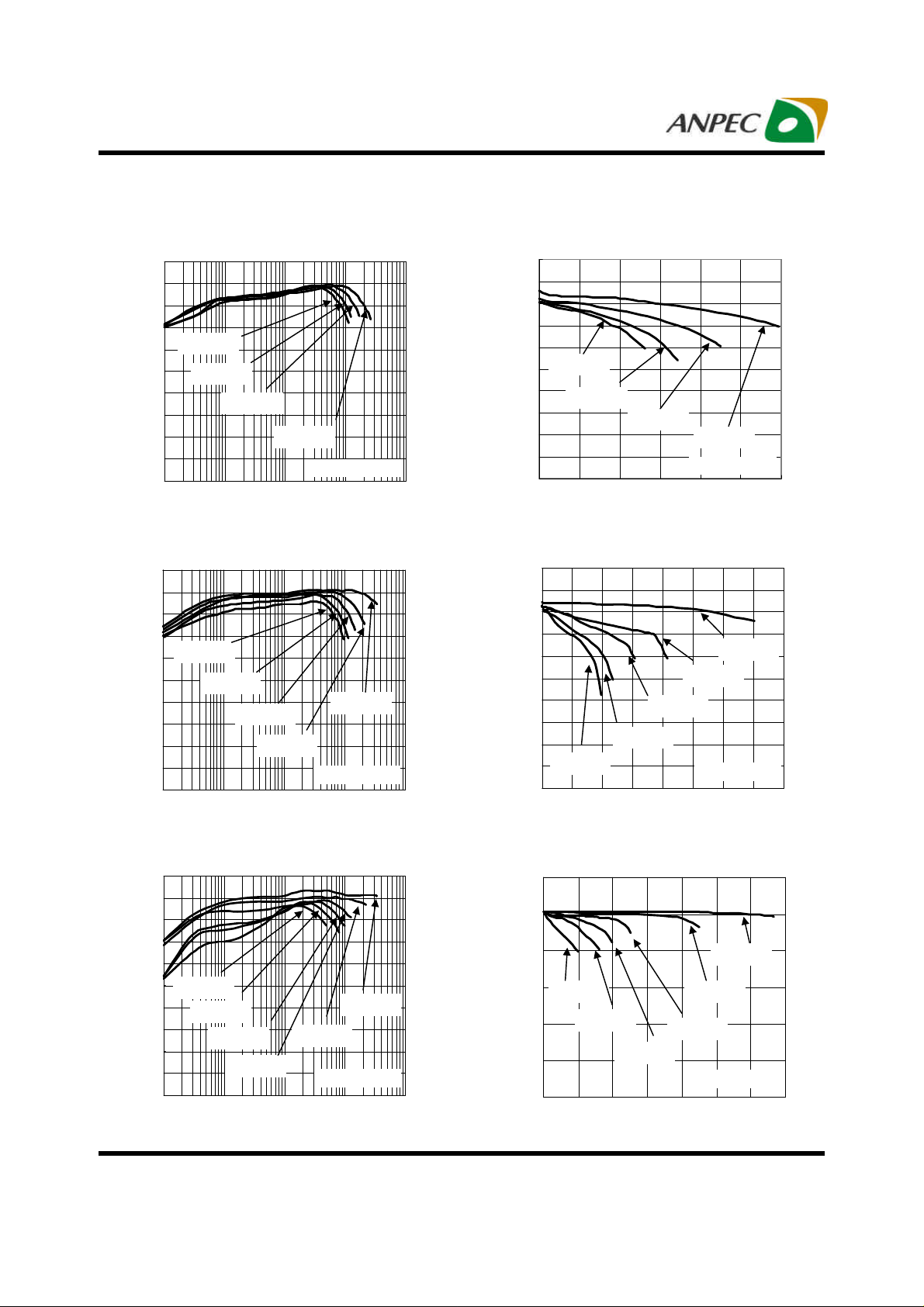
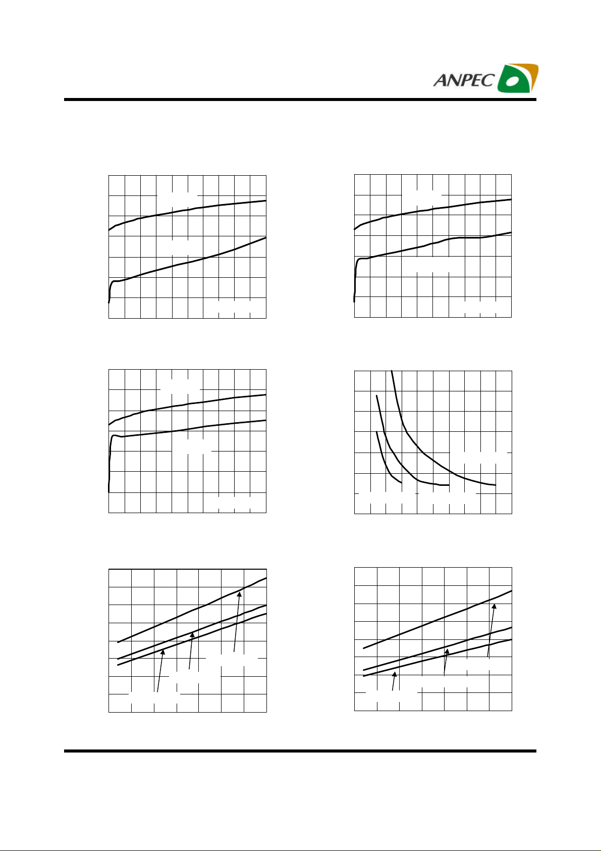
Typical Operating Characteristics
(Refer to the application circuit in the section “Typical Application Circuit”, VIN=1.5V, L1=22µH, TA=25oC unless otherwise noted.)
Efficiency vs. Output Current
100
90
80
70
VIN=0.9V
60
Efficiency (%)
50
40
30
20
10
0
VIN=1.0V
VIN=1.2V
VIN=1.5V
APW7079-18
0.1 1 10 100 1000
Output Current, I
OUT
(V)
OUT
Output Voltage, V
(mA)
Output Voltage vs. Output Current
1.84
1.82
1.80
1.78
1.76
1.74
1.72
1.70
1.68
1.66
1.64
VIN=0.9V
VIN=1.0V
VIN=1.2V
VIN=1.5V
APW7079-18
0 50 100 150 200 250 300
Output Current, I
OUT
(mA)
Efficiency vs. Output Current
100
90
80
70
VIN=0.9V
60
50
40
Efficiency (%)
30
20
10
0
0.1 1 10 100 1000
VIN=1.0V
VIN=1.2V
VIN=1.5V
Output Current, I
APW7079-30
OUT
Output Voltage vs. Output Current
100
90
80
70
60
50
VIN=0.9V
40
Efficiency (%)
30
20
10
0
VIN=1.0V
VIN=1.2V
VIN=1.5V
0.1 1 10 100 1000
Output Current, I
VIN=2.4V
APW7079-50
OUT
VIN=2.4V
(mA)
VIN=3.6V
(mA)
Output Voltage vs. Output Current
3.1
3.0
(V)
OUT
2.9
2.8
2.7
Output Voltage, V
VIN=0.9V
2.6
0 50 100 150 200 250 300 350 400
Output Voltage vs. Output Current
6
5
(V)
4
OUT
3
VIN=0.9V
2
Output Voltage, V
1
0
0 50 100 150 200 250 300 350
VIN=1.0V
Output Current, I
VIN=1.0V
VIN=1.2V
Output Current, I
VIN=1.2V
VIN=1.5V
VIN=2.4V
VIN=1.5V
APW7079-30
(mA)
OUT
VIN=3.6V
VIN=2.4V
APW7079-50
(mA)
OUT
Copyright ANPEC Electronics Corp.
Rev. A.4 - Jun., 2009
www.anpec.com.tw4
APW7079
Typical Operating Characteristics (Cont.)
(Refer to the application circuit in the section “Typical Application Circuit”, VIN=1.5V, L1=22µH, TA=25oC unless otherwise noted.)
Start-up/Hold-on Voltage vs.
Output Current
Start-up
1
Hold-on
(V)
HOLD
/V
ST
1.4
1.2
0.8
0.6
0.4
Start-up/Hold-on Voltage vs.
Output Current
Start-up
1
Hold-on
(V)
HOLD
/V
ST
1.4
1.2
0.8
0.6
0.4
0.2
Start-up/Hold-on Voltage, V
0
0 10 20 30 40 50
Output Current, I
Start-up/Hold-on Voltage vs.
1.4
(V)
1.2
HOLD
/V
1
ST
0.8
0.6
0.4
0.2
Start-up/Hold-on Voltage, V
0
0 10 20 30 40 50
Output Current
Start-up
Hold-on
Output Current, I
Main Switch ON Resistance vs.
Junction Temperature
(Ω)
N-FET
0.8
0.7
0.6
APW7079-18
(mA)
OUT
APW7079-50
(mA)
OUT
0.2
0
Start-up/Hold-on Voltage, V
0 10 20 30 40 50
Output Current, I
No Load Battery Current
70
60
(µA)
IN
50
40
30
20
10
No Load Battery Current, I
APW7079-18
0
0 0.5 1 1.5 2 2.5 3 3.5 4 4.5 5
vs. Input Voltage
Input Voltage, VIN (V)
Synchronous Switch ON Resis-
tance vs. Junction Temperature
1.6
1.4
1.2
APW7079-30
OUT
APW7079-50
APW7079-30
(mA)
0.5
0.4
0.3
0.2
0.1
0
Main Switch ON Resistance, R
APW7079-50
-50 -25 0 25 50 75 100 125
APW7079-30
APW7079-18
Junction Temperature, TJ (oC)
Copyright ANPEC Electronics Corp.
Rev. A.4 - Jun., 2009
1.0
0.8
(Ω)
P-FET
0.6
R
0.4
0.2
0.0
Synchronous Switch ON Resistance,
APW7079-50
-50 -25 0 25 50 75 100 125
APW7079-30
Junction Temperature, TJ (oC)
APW7079-18
www.anpec.com.tw5
APW7079
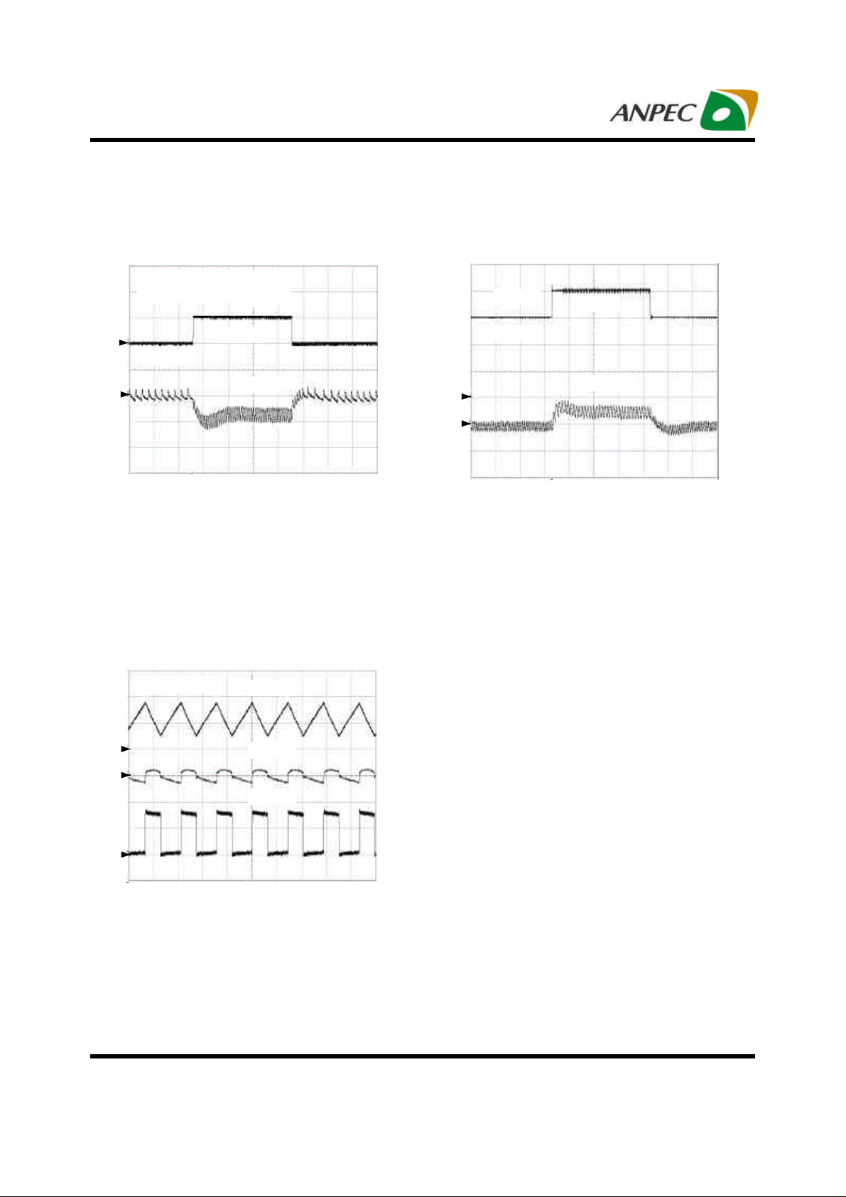
Operating Waveforms
Load Transient Response
I
=10mA -> 110mA -> 10mA
OUT
I
rise/fall time = 1µs
OUT
VIN=1.5V
2
110mA
I
OUT
10mA
V
3
CH2: I
CH3: V
, 100mA/Div, DC
OUT
, 50mV/Div, AC
OUT
OUT
Time: 0.1ms/Div
Heavy Load Switching Waveform
Line Transient Response
V
IN
1.5V
1
3
CH1: VIN, 0.5V/Div, DC
CH3: V
OUT
Time: 0.1ms/Div
, 50mV/Div, AC
2V
V
OUT
I
=100mA, VIN=1.5V
OUT
2
I
LX
V
OUT
3
V
LX
4
CH2: ILX, 200mA/Div, DC
CH3: V
, 50mV/Div, AC
OUT
CH4: VLX, 2V/Div, DC
Time: 5µs/Div
Copyright ANPEC Electronics Corp.
Rev. A.4 - Jun., 2009
www.anpec.com.tw6

APW7079
Pin Description
PIN FUNCTION
NO. NAME
1 LX
2 VOUT Converter output and control circuitry bias supply pin.
3 GND Ground.
Junction of N-FET and P-FET Drains. Connect the inductor here and minimize the trace area for
lowest EMI.
Block Diagram
0.9µs Min.
off-time
Comparator
4µs Max.
on-time
Error
-
+
V
REF
Thermal
Shutdown
Control
Logic
Soft
start
Zero Crossing
Comparator
+
-
Gate
Driver
Current Limit
Comparator
+
-
VOUT
2
1
GND
Synchronous
Switch
Main Switch
R
SENSE
3
LX
Typical Application Circuit
V
I
IN
IN
C1
22µF
Copyright ANPEC Electronics Corp.
Rev. A.4 - Jun., 2009
L1
22µH
APW7079
LX VOUT
GND
I
OUT
www.anpec.com.tw7

APW7079
Function Description
Control Scheme
The converter monitors the output voltage. When the internal feedback voltage falls below the reference voltage,
the main switch turns on and the induc tor current ramps
up. The main switch turns off when the current reaches
the peak current limit of typical 600mA. The second criterion that turns off the switch is the maximum on-time of
4µs (typical). As the main switch is turned off, the synchronous switch is turned on and delivers the current to
the output. The main switch remains off for a minimum of
900ns (typical), or until the internal feedback voltage drops
below the referenc e voltage. By the control scheme with
low quiescent current of 11µA (typical), the converter gets
high efficiency over a wide load range.
Start-Up
A startup oscillator circuit is integrated in the APW7079.
When the power is applied to the device, the circuit pumps
the output voltage high. Once the output voltage reaches
1.4V (typ), the main DC-DC circuitry turns on and boosts
the output voltage to the final regulation point.
Synchronous Rectification
The internal sync hronous rectifier eliminates the need
for an external Schottky diode, thus, reducing cost and
board space. During the cycle off-time, the P-channel
MOSFET turns on and shunts the MOSFET body diode.
As a result, the synchronous rectifier significantly improves
efficiency without the addition of an external component.
Conversion efficiency can be as high as 92%.
Over-Temperature Protection
The over-temperature circuit limits the junction temperature of the APW7079. When the junction temperature exceeds 150°C, a thermal sensor turns off the power
MOSFETs, allowing the devices to cool. The thermal sensor allows the converter to start a start-up process and
regulate the output voltage again after the junction temperature cools by 40°C. The OTP is designed with a 40°C
hysteresis to lower the average TJ during continuous thermal overload conditions, increasing lifetime of the device.
Copyright ANPEC Electronics Corp.
Rev. A.4 - Jun., 2009
www.anpec.com.tw8

APW7079
Application Information
Input Capacitor Selection
The input capacitor is chosen based on the voltage rating
and the RMS current rating. For reliable operation, it is
recommended to selec t the capacitor voltage rating at
least 1.3 times higher than the maximum input voltage.
The maximum RMS current rating of the input capacitor is
calculated as the following equation:
TV
I
RMS
1
⋅
ONIN
⋅=
L
3
where
T
= main switch max. on-time (4µs typical)
ON
VIN = input voltage
L = inductor value in µ H
The capacitors should be placed close to the inductor
and the GND.
Output Capacitor Selection
An output capacitor is required to filter the output and supply the load transient current. The output ripple is the sum
of the v oltages across the ESR and the ideal output
capacitor. The peak-to-peak voltage of the ESR is c alculated as the following equations:
ESR x I V PEAKESR =∆
IV
⋅
I ≤
=
PEAK
OUTOUT
V
η⋅
IN
TV
⋅
ONIN
+
I
LIM
L2
⋅
Where
I
= peak current of inductor in amp
PEAK
η= efficiency (0.85 typical)
The peak-to-peak voltage of the ideal output capacitor is
calculated as the following equation:
ONOUT
COUT
=∆
For the applications using tantalum capacitors, the ∆V
is much smaller than the V
Therefore, the AC peak-to-peak output voltage (∆V
TIV×
OUT
C
COUT
and can be ignored.
ESR
) is
OUT
shown as below:
ESR x I V PEAKOUT =∆
Since the output ripple is the product of the peak inductor
current and the output capacitor ESR, using low-ESR tantalum capacitors for the best performance or connecting
two or more filter capacitors in parallel is recommended.
Inductor Selection
The inductor value determines the inductor ripple current
and affects the load transient response. It is recommended to select the boost inductor in order to keep the
maximum peak inductor current below the current limit
threshold of the power switch. For example, the current
limit threshold of the APW7079’s switch is 600mA. For
choosing an inductor which has peak current passed,
firstly, it is necessary to consider the output load (I
input (VIN), and output voltage (V
). Secondly, the de-
OUT
OUT
sired current ripple in the inductor also needed to be
taken into account. The current was calculated in “Output
Capacitor Selection”. Since the output ripple is the product of the peak inductor current and the output capacitor
ESR, the larger inductor value reduces the inductor current ripple and output voltage ripple but typically offers a
larger physical size.
The inductor value also slightly affects the maximum output current. The maximum output current can be calculated as below:
V
I
IN
)MAX(OUT
V
OUT
−=
TI
OFFLIM
−
VV
INOUT
η⋅
×
L2
where
T
= main switch min. off-time (0.9µs typical)
OFF
Therefore, to consider the balance of the efficiency and
component size, an inductor value of 22µH to 47µH is
recommended in most applications.
I
V
I
IN
IN
C
IN
LX
N-FET
LX
I
I
SWP
SWN
P-FET
I
OUT
ESR
V
OUT
C
OUT
),
Copyright ANPEC Electronics Corp.
Rev. A.4 - Jun., 2009
www.anpec.com.tw9

APW7079
Application Information (Cont.)
I
LX
I
LIM
I
PEAK
I
IN
I
SWN
I
SWP
V
OUT
V
OUT
I
PEAK
x ESR
RAJ T + T = T
where
TA = the ambient temperature.
The power dissipation can be calculated as below:
PD = P
x (1-η)/η
OUT
where
P
= Output power (V
OUT
OUT
x I
OUT
)
η = Efficiency
As an example, the APW7079-18 converts an input voltage 1.2V to provide a load current of 175mA at ambient
temperature of 85°C. Assume the efficiency (η) is 0.75.
Therefore, the power dissipated on the converter is:
PD = 1.8 x 0.175 x (1-0.75)/0.75= 0.105 Watt
I
OUT
Since the power dissipation includes the loss of external
components, the actual value is s lightly lower. For the
SOT-89 package, the
θ
is 180°C/W. Thus, the junction
JA
temperature of the regulator is as below:
Thermal Consideration
In mos t applications, the APW7079 does not dissipate
much heat due to its high efficiency. However, in applications where the APW7079 is running at high ambient temperature with low output voltage, the heat dissipated may
exceed the maximum junction temperature of the part. If
the junction temperature reaches approximately 150°C,
both power switches will be turned off and the LX node
will become high impedance. To avoid the APW7079 from
exceeding the maximum junc tion temperature, the user
will need to do some thermal analysis. The goal of the
thermal analysis is to determine whether the power dissipated exceeds the maximum junction temperature of
the part. The temperature rise is given by:
TR = (PD)(θJA)
where PD is the power dissipated by the regulator and θ
JA
is the thermal resistance from the junction of the die to
the ambient temperature. The junction temperature, TJ,
is given by:
TJ = 85°C + (PD)(180) = 104 °C
The maximum junction temperature s hould be less than
125°C. Note that, the junction temperature is lower at
higher output voltages due to reduced switch resistance.
Layout Consideration
For all switching power supplies especially with high peak
currents and switching frequency, the layout is an important step in the design. If the layout is not carefully done,
the regulator may show nois e problems and duty cycle
jitter.
1.The input capacitor should be placed close to the
device, which can reduce copper trace resistance and
effect input ripple of the IC.
2.The inductor should be placed as close as possible to
the switch pin to minimize the switching noise.
3.The output capacitor should be placed closed to the
VOUT and the GND.
Copyright ANPEC Electronics Corp.
Rev. A.4 - Jun., 2009
www.anpec.com.tw10

APW7079
Application Information (Cont.)
Layout Consideration (Cont.)
Copyright ANPEC Electronics Corp.
Rev. A.4 - Jun., 2009
www.anpec.com.tw11

APW7079
Pack age Information
SOT-89
B1
S
Y
M
B
O
L
A
B
B1
C
D
D1
E
E1
e
e1
H
L 0.89
MIN. MAX.
1.40
0.44
0.36 0.48
0.35 0.44
4.40 4.60
1.62 1.83
2.29 2.60
2.13
3.94 4.25
D
D1
EL
H
e
e1
B
SOT-89
MILLIMETERS
1.60
0.56
2.29
1.50 BSC 0.059 BSC
3.00 BSC
1.20
E1
INCHES
MIN. MAX.
0.055
0.017
0.014 0.019
0.014 0.017
0.173 0.181
0.064 0.072
0.090 0.102
0.084
0.118 BSC
0.155 0.167
0.035
A
C
0.063
0.022
0.090
0.047
Copyright ANPEC Electronics Corp.
Rev. A.4 - Jun., 2009
Note : Follow JEDEC TO-243 AA.
www.anpec.com.tw12

APW7079
Carrier Tape & R eel Dimensions
OD0
B0
P0
P2
P1
A
E1
F
W
Application
SOT-89
K0
SECTION A-A
B
A
H
A0
SECTION B-B
OD1
B
T
A
d
T1
A H T1 C d D W E1 F
178.0±2.00 50 MIN.
12.4+2.00
-0.00
13.0+0.50
-0.20
1.5 MIN. 20.2 MIN. 12.0±0.30 1.75±0.10 5.50±0.05
P0 P1 P2 D0 D1 T A0 B0 K0
4.0±0.10 8.0±0.10 2.0±0.05
1.5+0.10
-0.00
1.5 MIN.
0.6+0.00
-0.40
4.80±0.20 4.50±0.20 1.80±0.20
(mm)
Devices Per Unit
Package Type Unit Quantity
SOT-89
Copyright ANPEC Electronics Corp.
Rev. A.4 - Jun., 2009
Tape & Reel 1000
www.anpec.com.tw13

APW7079
Taping Direction Information
SOT-89
USER DIRECTION OF FEED
Classification Profile
Copyright ANPEC Electronics Corp.
Rev. A.4 - Jun., 2009
www.anpec.com.tw14

APW7079
Classification Reflow Profiles
Profile Feature Sn-Pb Eutectic Assembly Pb-Free Assembly
Preheat & Soak
Temperature min (T
Temperature max (T
Time (T
smin
to T
smax
smin
smax
) (ts)
)
)
Average ramp-up rate
(T
to TP)
smax
Liquidous temperature (TL)
Time at liquidous (tL)
Peak package body Temperature
(Tp)*
Time (tP)** within 5°C of the specified
classification temperature (Tc)
Average ramp-down rate (Tp to T
smax
Time 25°C to peak temperature
See Classification Temp in table 1 See Classification Temp in table 2
)
100 °C
150 °C
60-120 seconds
150 °C
200 °C
60-120 seconds
3 °C/second max. 3°C/second max.
183 °C
60-150 seconds
217 °C
60-150 seconds
20** seconds 30** seconds
6 °C/second max. 6 °C/second max.
6 minutes max. 8 minutes max.
* Tolerance for peak profile Temperature (Tp) is defined as a supplier minimum and a user maximum.
** Tolerance for time at peak profile temperature (tp) is defined as a supplier minimum and a user maximum.
Table 1. SnPb Eutectic Process – Classification Temperatures (Tc)
Package
Thickness
<2.5 mm
Volume mm
3
Volume mm
<350
235 °C 220 °C
≥350
3
≥2.5 mm 220 °C 220 °C
Table 2. Pb-free Process – Classification Temperatures (Tc)
Package
Thickness
<1.6 mm
1.6 mm – 2.5 mm
Volume mm3
<350
Volume mm3
350-2000
Volume mm3
260 °C 260 °C 260 °C
260 °C 250 °C 245 °C
>2000
≥2.5 mm 250 °C 245 °C 245 °C
Reliability Test Program
Test item Method Description
SOLDERABILITY JESD-22, B102
HOLT JESD-22, A108
PCT JESD-22, A102
TCT JESD-22, A104
HBM MIL-STD-883-3015.7
MM JESD-22, A115
Latch-Up JESD 78
Copyright ANPEC Electronics Corp.
Rev. A.4 - Jun., 2009
5 Sec, 245°C
1000 Hrs, Bias @ 125°C
168 Hrs, 100%RH, 2atm, 121°C
500 Cycles, -65°C~150°C
VHBM≧2KV
VMM≧200V
10ms, 1tr≧100mA
www.anpec.com.tw15

APW7079
Customer Service
Anpec Electronics Corp.
Head Office :
No.6, Dusing 1st Road, SBIP,
Hsin-Chu, Taiwan, R.O.C.
Tel : 886-3-5642000
Fax : 886-3-5642050
Taipei Branch :
2F, No. 11, Lane 218, Sec 2 Jhongsing Rd.,
Sindian City, Taipei County 23146, Taiwan
Tel : 886-2-2910-3838
Fax : 886-2-2917-3838
Copyright ANPEC Electronics Corp.
Rev. A.4 - Jun., 2009
www.anpec.com.tw16

 Loading...