ANPEC APW7060KC-TU, APW7060KC-TR Datasheet

APW7060
Dual Controllers - Step Down Synchronous PWM and Linear Controller
Features
••
Provides Two Regulated Voltages
•
••
- One Synchronous DC/DC Buck Controller
- One Linear Controller
••
0.8V Internal Reference Voltage
•
••
- Both Controllers: 0.8V ± 2% Line, Load
and Temp.
••
Output Voltage Range
•
••
- PWM Controller : 0.8V to V
- Linear Controller : 0.8V to (12VCC-V
••
• Full Duty Cycle Range for PWM Controller
••
IN
)
GSpass
- 0% to 100%
••
• Internal Loop Compensation for PWM Controller
••
••
• Internal 2ms Soft Start and Short Circuit Protec
••
tion for both Controllers
••
• Both Controllers Drive N-Channel MOSFETs
••
••
• Small Converter Size
••
- 600kHz Constant Switching Frequency
- Simple SO-14 Package
••
• Shutdown Control
••
Applications
••
• Motherboard
••
••
• Graphics Cards
••
General Description
The APW7060 integrates a synchronous buck PWM
controller and a linear controller to provide two regulated voltages in a single package. The PWM controller drives external N-channel MOSFETs and operates
at a fixed 600kHz frequency. When the input supply
drops close to the output, the upper MOSFET remains
on, achieving 100% duty cycle. Internal loop compensation is optimized for fast transient response, eliminating external compensation network. The linear controller drives an external N-channel MOSFET to form a
linear regulator. The internal 0.8V reference makes this
part suitable for a wide variety of low voltage
applications.
The APW7060 has an undervoltage lockout circuitry
to ensures that both the 5VCC and 12VCC must be
present before its internal circuitry is power up. Soft
start is internally set to 2ms and will bring both outputs into regulation in a controlled manner. When either output goes into short, soft start will be initiated.
If the short condition still remains after three cycles,
both regulators will be shut down. To restart both
regulators, recycle the voltage at 5VCC or 12VCC pin
or momentarily pull the FB2 pin above 1.28V.
The APW7060 can be shutdown by pulling the FB2
pin above 1.28V. In shutdown, all gate drive signals
will be low. This dual controller is available in SO-14
package.
Pinouts
FB2
NC
1
2
3
4
5
6
7
••
• 12V , 5V and 3.3V Inputs DC-DC Converter
••
••
• DSP Supplies
••
••
• Embedded processor and I/O supplies
••
ANPEC reserves the right to make changes to improve reliability or manufacturability without notice, and advise
customers to obtain the latest version of relevant information to verify before placing orders.
Copyright ANPEC Electronics Corp.
Rev. A.3 - Oct., 2003
LGATE
GND
GND
5VCC
DRIVE2
UGATE
14
13
12VCC
NC
12
NC
11
NC
10
FB
9
NC
8
www.anpec.com.tw1

APW7060
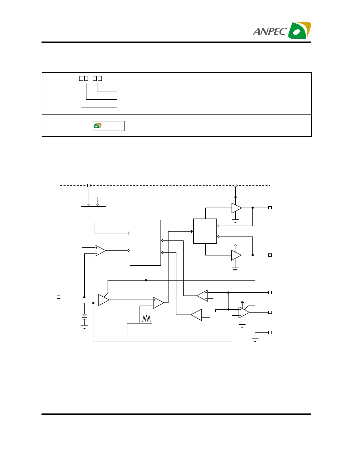
Ordering and Marking Information
APW 7060
APW7060 K :
APW7060
XXXXX
Block Diagram
5VCC
Under
Voltage
Lockout
UVLO
0.5V
Handling Code
Temp. Range
Package Code
UVP1
Soft-Start
and Fault
Logic
Packag e Cod e
K : S OP-1 4
Operating Junction Temp. Range
C : 0 to 7 0 °C
Handling Code
TU : T u be
TR : T a pe & R e e l
XXXXX - Date Code
12VCC
PWM
Gate
Control
UGATE
5VCC
LGATE
FB
VREF
0.8V
COMP
Error
Amplifier
Copyright ANPEC Electronics Corp.
Rev. A.3 - Oct., 2003
Inhibit /
Soft-Start
Os c illa t or
.ECKH/Figure 1.
F
OSC
600kHz
UVP2
Shutdown
0.5V
1.28V
12VCC
Linear
Controller
FB2
DRIVE2
GND
www.anpec.com.tw2

APW7060
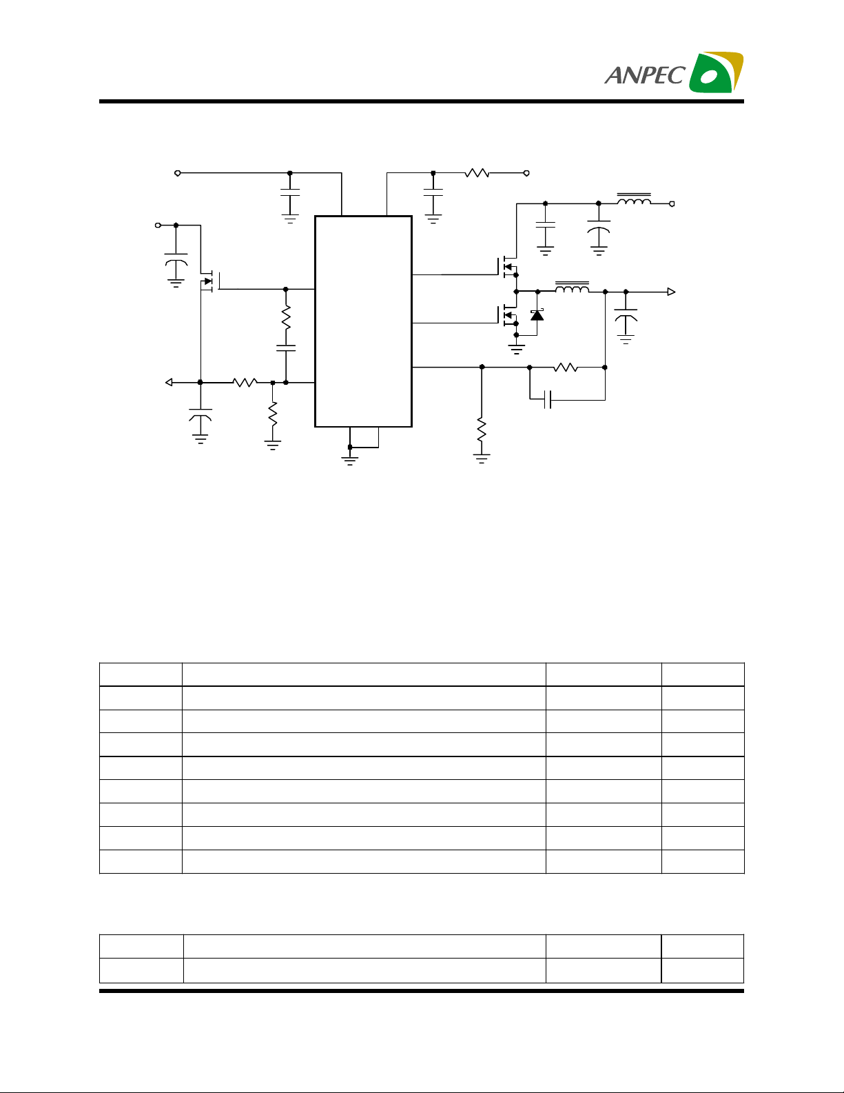
Typical Application
+12V
V
IN2
+3.3V
C10
470uF
V
OUT2
+2.5V/3A
C11
470uF
Q1 : APM2014N UC
Q2 : APM2014N UC
Q3 : APM2055N UC
D1 : 3A Schottky Diode
C2, C3, C5, C6, C10, C1 1 : 470uF/6.3V, ESR=30mΩ
Q3
R10
6.8k
C9
470pF
R7
2.37k R8
1.13k
C8
1uF
5
6
12VC C
DR IVE2
FB2
13
U1
APW 7060
GND
2
5VC C
UGATE
LGATE
GND
R4
+5V
2.2
C1
4
1uF
C4
4.7uF
Q1
14
L1
1uH
L2
1uH
C2, C3
2 x 470uF
V
IN1
+3.3V
V
OUT1
+1.263V
1
Q2
9
FB
3
R2
1.02k
D1
C7
68nF
C5, C6
2 x 470uF
R1
590
/10A
.ECKH/Figure 2.
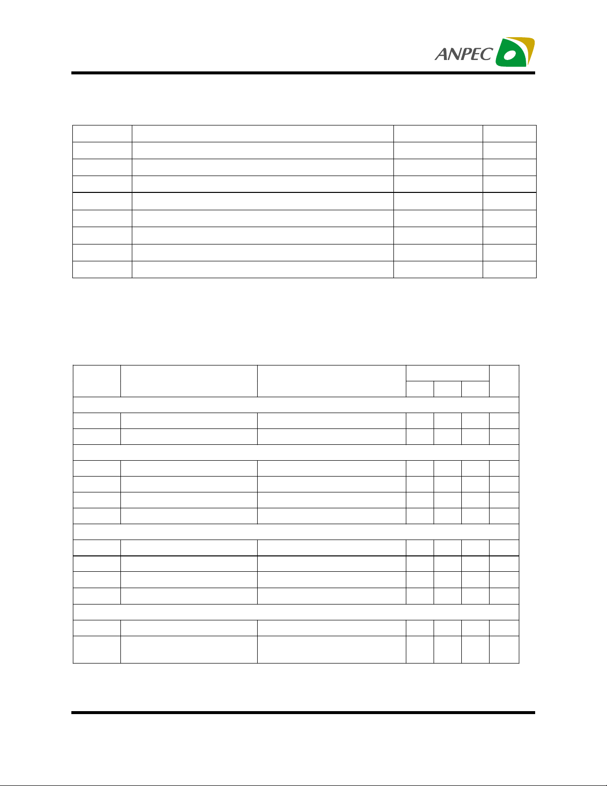
Absolute Maximum Ratings
Symbol Parameter Rating Unit
5V
12V
5VCC Supply Voltag e ( 5 V CC to GND) -0.3 ~ 7 V
CC
12VCC Supply Voltage (12VCC to GND) -0.3 ~ 15 V
CC
UAGTE, DRIVE2 to GND -0.3 ~ 12V
LGATE, FB, FB2 to GND -0.3 ~ 5V
CC
CC
Maximum Junction Temperature 150
T
STG
T
SDR
V
ESD
Storage Temperature -65 ~ 150
Maximum Soldering Temperature, 10 Seconds 300
Minimum ESD R ating (Human b ody model)
2
±
Thermal Characteristics
Symbol Parameter Value Unit
JA
θ
Junction-to-Ambient Resistance in free air (SOP-14) 160
o
o
o
KV
o
C/W
V
V
C
C
C
Copyright ANPEC Electronics Corp.
Rev. A.3 - Oct., 2003
www.anpec.com.tw3

APW7060
Recommended Operating Conditions
(Note)
Symbol Parameter Range Unit
CC
5V
12V
OUT1
V
V
OUT2
V
V
T
T
IN1
IN2
A
5VCC Supply Voltage
CC
12VCC Supply Voltage
5 ± 5%
12 ± 10%
Output Voltage of the Buck converter 0.8 ~ 3.3 V
Input Voltage of the Buck converter
3.3/5 ± 5%
Output Voltage of the Linear Regulator 0.8 ~ 3.3 V
Input Voltage of the Linear Regulator
3.3/5 ± 5%
Ambient Temperature 0 ~ 70
J
Junction Temperature 0 ~ 125
V
V
V
V
o
C
o
C
Note : Refer to the typical application circuit
Electrical Characteristics
Unless otherwise specified, these specifications apply over 5VCC=5V, 12VCC=12V and TA= 0~70 oC. Typical
values are at TA=25oC.
APW7060
Symbol Parameter Test Conditions
Min Typ Max
SUPPLY CURRENT
ICC 5VCC Supply Current
12VCC Supply Current
LGATE Open, FB2=DRIVE2
UGATE Open
2.5 mA
2.5 mA
UNDER VOLTAGE LOCKOUT
Rising 5VCC Threshold 12VCC=12V 4.0 4.2 4.4 V
Falling 5VCC Threshold 12VCC=12V 3.5 3.7 3.9 V
Rising 12VCC Threshold 5VCC=5V 9.6 10.3 10.8 V
Falling 12VCC Threshold 5VCC=5V 9.3 9.7 10.2 V
OSCILLATOR
OSC
F
Free Running Frequency 550 600 650 kHz
Ramp Upper Threshold 2.85 V
Ramp Lower Threshold 0.95 V
Ramp Amplitude 1.9 V
OSC
∆V
REFERENCE VOL TAGE
REF
V
Reference Voltage 0.8 V
System Accura cy
Over Line, Load and
Temperature
-2 +2 %
Unit
P-P
Copyright ANPEC Electronics Corp.
Rev. A.3 - Oct., 2003
www.anpec.com.tw4

APW7060
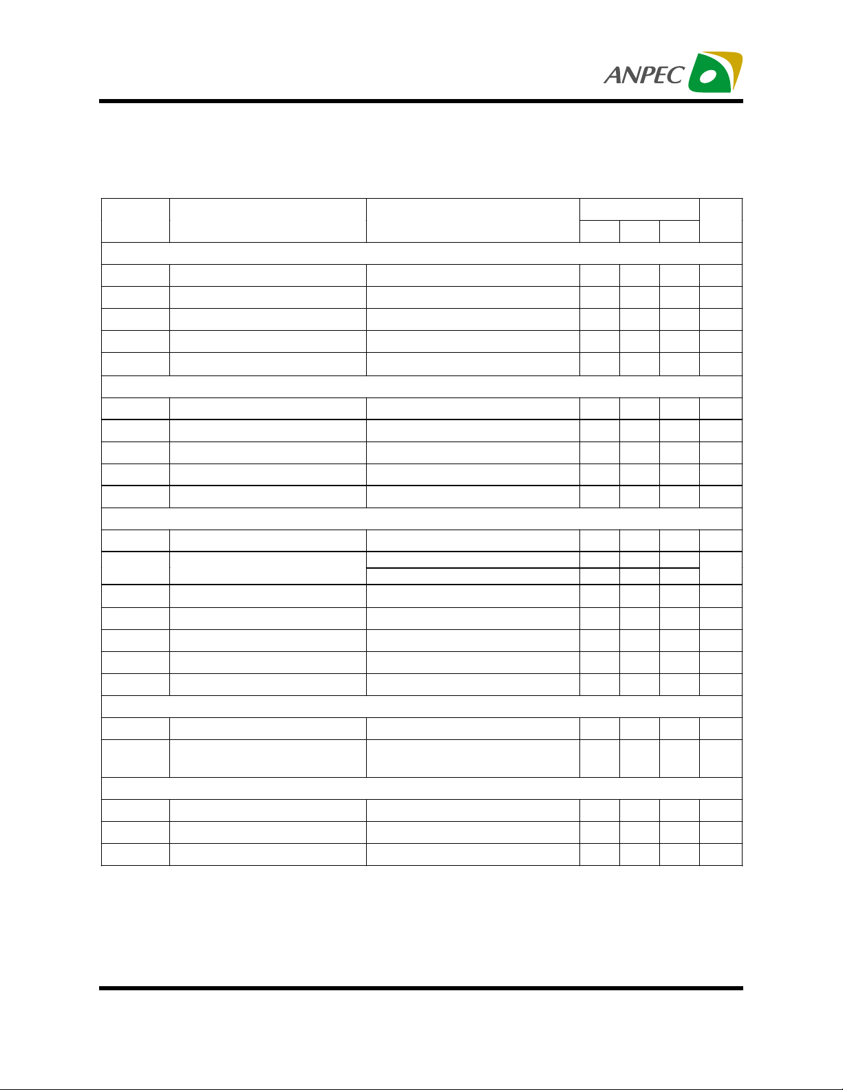
Electrical Characteristics (Cont.)
Unless otherwise specified, these specifications apply over 5VCC=5V, 12VCC=12V and TA= 0~70 oC. Typical
values are at TA=25oC.
Symbol Parameter Test Conditions
BUILT-IN PWM FEEDBACK COMPENSATION
DC Gain 75 dB
P
F
F
First Pole Frequency 10 Hz
Z
First Zero Frequency 1
UGATE Duty Range 0 100 %
FB Input Current
PWM CONTROLLER GATE DRIVERS
UGATE Source V
UGATE Sink
LGATE Source V
LGATE Sink V
D
T
Dead Time 50
UAGTE
=1V 0.6 A
UGATE
V
=1V 7.3
LGATE
=1V 0.6 A
LGATE
=1V 1.8
LINEAR CONTROLLER
DC Gain 78 dB
Gain Bandwidth Product
CL=0.5nF 1.6
L
C
=1nF 1
FB Input Current 0.1
DRIVE2 S ourc e C ur re nt V
DRIVE2 Sink Current V
FB2=VREF
FB2=VREF
-20mV, V
+20mV, V
DRIVE2
DRIVE2
DRIVE2 Output High Vo ltage DRIVE2 Open 11.7 V
DRIVE2 Output Low Voltage DRIVE2 Ope n 0.01 V
UNDER-VOLTAGE PROTECTION
FB
UV
FB/FB2 Under-Voltage Level FB or FB2 Falling 0.5 V
FB/FB2 Under-Voltage
Hysteresis
15 mV
SOFT-START AND SHUTDOWN
SS
T
Soft-Start Interval 2 mS
FB2 Shutdown Threshold FB2 Rising 1.28 V
FB2 Shutdown Hysteresis 30 mV
APW706 0
Unit
Min Typ Max
kHz
0.1
µA
Ω
Ω
nS
MHz
µA
=7V 9.8 mA
=3V 2.6
mA
Copyright ANPEC Electronics Corp.
Rev. A.3 - Oct., 2003
www.anpec.com.tw5
 Loading...