ANPEC APW7058KC-TU, APW7058KC-TR Datasheet

APW7058
Synchronous Buck PWM and Linear Controllers
Features
••
•
Provides Two Regulated Voltages
••
- One Synchronous-Rectified Buck PWM
Controller
- One Linear Controller
••
•
Low Reference Voltage for Further Applications
••
- Both Controllers : 0.8V ± 2% Over
Temperature
••
• Both Controllers Drive N-Channel MOSFETs
••
- PWM Controller Drives Dual N-Channel
MOSFETs
- Linear Controller Drives N-Channel MOSFET
••
• Built-in PWM Feedback Compensation
••
- No Steady-State Error
- Voltage-Mode PWM Control
- Full 0~100% Duty Ratio
- Fast Transient Response
••
• Adjustable Outputs by External Resistor Dividers
••
••
• Under-Voltage Monitoring on Both Controllers
••
••
• Small Converter Size
••
- 600kHz Constant Switching Frequency
- Built-In Soft-Start
- Simple SO-8 Package
General Description
The APW7058 integrates one synchronous-rectified
Buck PWM controller and one linear controller to pro-
vide two regulated voltages for graphics cards and
other embedded processor applications. The PWM
controller which drives dual N-channel MOSFETs uses
fixed 600kHz frequency, voltage-mode PWM control
and integrates power-on-reset(POR), built-in soft-start,
output under-voltage monitoring and shutdown func-
tions into a single chip. The linear controller which
drives a N-channel MOSFET bypass transistor allows
users to optimize the transient response by external
components. The POR circuit with hysteresis moni-
tors both 5VCC and 12VCC supply voltages to start
up/shutdown the IC at power-on/off. An internal 0.8V
temperature-compensated reference is designed to
meet the low output voltage requirement for further
applications. The built-in soft-start function sets the
soft-start interval to prevent the output voltages from
overshoot as well as limiting the input currents. The
under-voltage protections monitor the voltages at FB
and FB2 for short-circuit protection. The under-volt-
age protections cycle the soft-start function until 3
times of UVP events are happened. Pulling and hold-
ing the FB2 pin above 1.28V to disable the both
controllers.
••
• Shutdown Control
••
Pin Description
Applications
12VCC
••
• Motherboard
••
••
• Graphics Cards
••
••
• 12V, 5V and 3.3V Inputs DC-DC Converter
••
ANPEC reserves the right to make changes to improve reliability or manufacturability without notice, and advise
customers to obtain the latest version of relevant information to verify before placing orders.
Copyright ANPEC Electronics Corp.
Rev. A.2 - Jun., 2003
UGATE
GND
LGATE 5VCC
1
2
3
45
FB
8
FB2
7
DRIVE2
6
www.anpec.com.tw1

APW7058
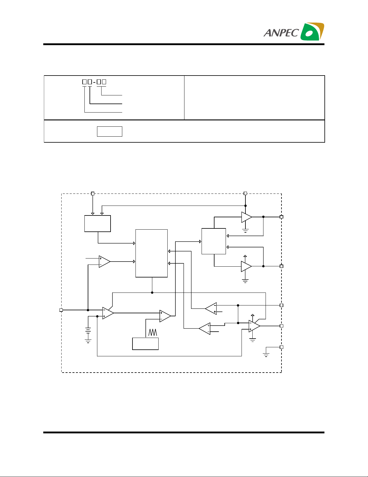
Ordering and Marking Information
APW7058
APW7058 K :
APW7058
XXXXX
Block Diagram
5VCC
Power
On Reset
POR
0.5V
Handling Code
Temp. Range
Package Code
UVP1
Soft-Start
and Fault
Logic
Package Code
K : S O P - 8
Operating Junction Temp. Range
C : 0 to 70 °C
Handling Code
TU : Tu be
TR : Ta pe & R eel
XXXXX - Date Code
12VCC
PWM
Gate
Control
UGATE
5VCC
LGATE
FB
VREF
0.8V
COMP
Error
Am plifier
Copyright ANPEC Electronics Corp.
Rev. A.2 - Jun., 2003
Inhibit /
Soft-S tart
Oscillator
F
OSC
600kHz
UVP2
Shutdown
0.5V
1.28V
12VCC
Linear
Controller
FB2
DRIVE2
GND
www.anpec.com.tw2

APW7058
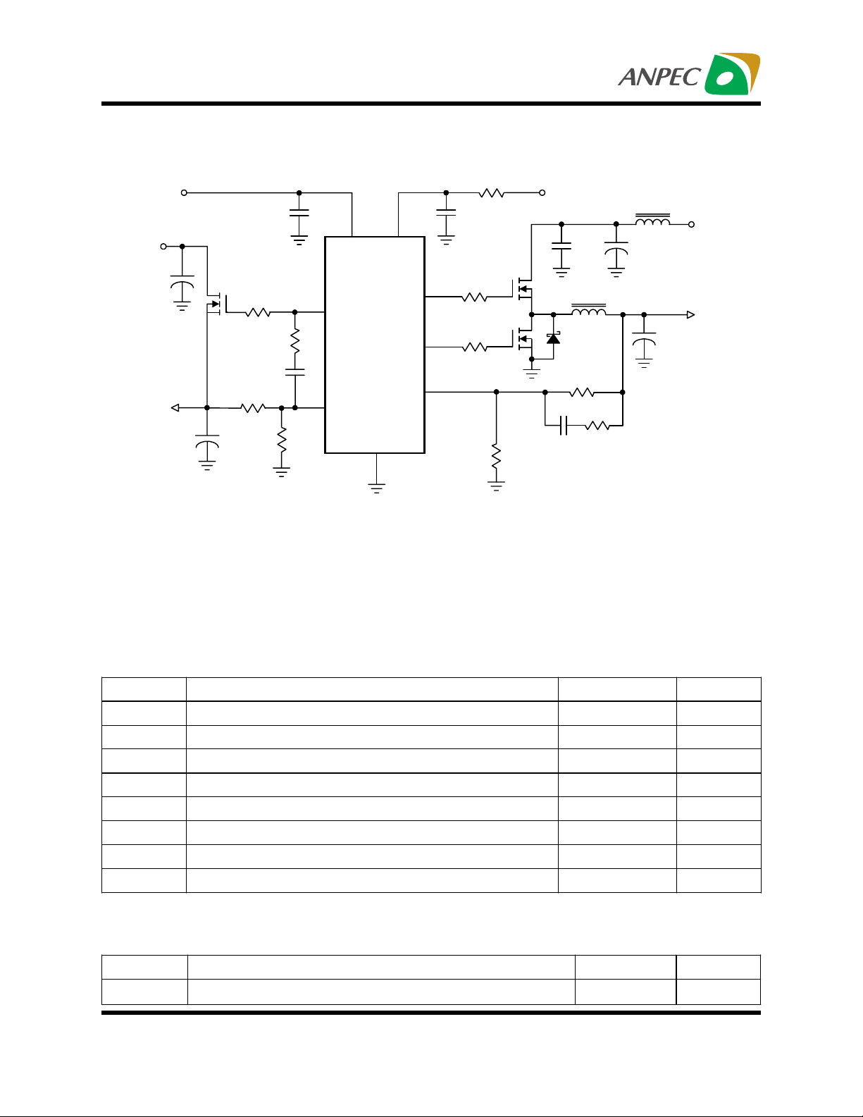
Typical Application
+12V
IN2
V
+3.3V
C10
470uF
OUT2
V
+2.5V/3A
C8
C11
470uF
Q3
R9
0
R7
2.37k
R10
27k
C9
33pF
R8
1.13k
1uF
6
7
12VCC
DRIVE2
FB2
1
5VCC
U1
APW7058
GND
3
5
UGATE
LGATE
FB
1uF
2
4
8
Q1, Q2 : APM2014N UC
D1 : 3A Schcottky Diode
Q3 : APM2055N UC
C2, C3, C5, C6, C10, C11 : 470µF/6.3V, ESR=30mΩ
C1
R5
R6
R4
+5V
2.2
C4
4.7uF
Q1
0
L1
1uH
L2
1uH
C2, C3
2 x 470uF
IN1
V
+3.3V
OUT1
V
+1.263V
0
Q2
R2
1.02k
D1
C7
68nF
R1
590
R3
C5, C6
2 x 470uF
0
/10A
Absolute Maximum Ratings
Symbol Parameter Rating Unit
5V
12V
5VCC Supply Voltage (5VCC to GND) -0.3 ~ 7 V
CC
12VCC Supply Voltage (12VCC to GND) -0.3 ~ 15 V
CC
UAGTE, DRIVE2 to GND -0.3 ~ 12V
LGATE, FB, FB2 to GND -0.3 ~ 5V
CC
CC
Maximum Junction Temperature 150
T
STG
T
SDR
V
ESD
Storage Temperature -65 ~ 150
Maximum Soldering Temperature, 10 Seconds 300
Minimum ESD Rating (Human body model)
2
±
Thermal Characteristics
Symbol Parameter Value Unit
JA
θ
Copyright ANPEC Electronics Corp.
Rev. A.2 - Jun., 2003
Junction-to-Ambient Resistance in free air (SOP-8) 160
www.anpec.com.tw3
o
o
o
KV
o
C/W
V
V
C
C
C

APW7058
Recommended Operating Conditions
(Note)
Symbol Parameter Range Unit
CC
5V
12V
OUT1
V
V
OUT2
V
V
T
T
IN1
IN2
A
5VCC Supply Voltage
CC
12VCC Supply Voltage
5 ± 5%
12 ± 10%
Output Voltage of the Buck converter 0.8 ~ 3.3 V
Input Voltage of the Buck converter
3.3/5 ± 5%
Output Voltage of the Linear Regulator 0.8 ~ 3.3 V
Input Voltage of the Linear Regulator
3.3/5 ± 5%
Ambient Temperature 0 ~ 70
J
Junction Temperature 0 ~ 125
V
V
V
V
o
C
o
C
Note : Refer to the typical application circuit
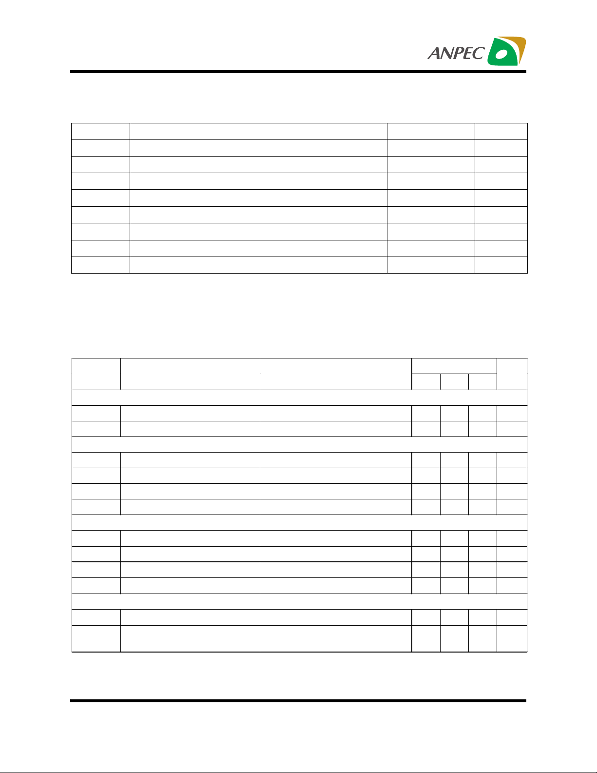
Electrical Characteristics
Unless otherwise specified, these specifications apply over 5VCC=5V, 12VCC=12V and TA= 0~70 oC. Typical
values are at TA=25oC.
Symbol Parameter Test Conditions
SUPPLY CURRENT
CC
I
5VCC Supply Current LGATE Open, FB2=DRIVE2 2.5 mA
12VCC Supply Current UGATE Open 2.5 mA
POWER-ON RESET
Rising 5VCC Threshold 12VCC=12V 4.0 4.2 4.5 V
Falling 5VCC Threshold 12VCC=12V 3.5 3.7 3.9 V
Rising 12VCC Threshold 5VCC=5V 9.6 10.3 10.8 V
Falling 12VCC Threshold 5VCC=5V 9.3 9.7 10.2 V
OSCILLATOR
OSC
F
Free Running Frequency 550 600 650 kHz
Ramp Upper Threshold 2.85 V
Ramp Lower Threshold 0.95 V
Ramp Amplitude 1.9 V
OSC
∆V
REFERENCE VOLTAGE
REF
V
Reference Voltage 0.8 V
System Accuracy
Over Line, Load and
Temperature
APW7058
Min Typ Max
-2 +2 %
Unit
P-P
Copyright ANPEC Electronics Corp.
Rev. A.2 - Jun., 2003
www.anpec.com.tw4
 Loading...