ANPEC APW7057KC-TU, APW7057KC-TR Datasheet

APW7057
High Power Step-Down Synchronous DC/DC Controller
Features
••
Operates from +5V Input
•
••
••
0.8V Internal Reference Voltage
•
••
- ±1.5% Accuracy Over Line, Load and Temp.
••
0.8V to VCC Output Range
•
••
••
Full Duty Cycle Range
•
••
- 0% to 100%
••
Internal Loop Compensation
•
••
••
Internal Soft Start
•
••
- Typical 2ms
••
• Programmable Over-Current Protection
••
- Lossless Sensing Using MOSFET R
••
• Under-Voltage Protection
••
••
• Drives External N-Channel MOSFETs
••
••
• Shutdown Control
••
••
• Small SOP-8 Package
••
DS (ON)
Applications
••
• Motherboard
••
••
• Graphics Cards
••
••
• Cable or DSL Modems, Set Top Boxes
••
••
• DSP Supplies
••
General Description
The APW7057 is a 300kHz constant frequency voltage mode synchronous switching controller that drives
external N-channel MOSFETs. When the input supply drops close to output, the upper MOSFET remains
on, achieving 100% duty cycle. Internal loop compensation is optimized for fast transient response, eliminating external compensation network. The precision
0.8V reference makes this part suitable for a wide variety of low voltage applications. Soft start is internally
set to 2ms, limiting the input in-rush current and preventing the output from overshoot during powering up.
The APW7057 has over current and short circuit
protections. Over current protection is achieved by
monitoring the voltage drop across the high side
MOSFET, eliminating the need for a current sensing resistor and short circuit condition is detected
through the FB pin. If either fault conditions occur,
the APW7057 would initiate the soft start cycle. After
three cycles and if the fault condition persists, the
controller will be shut down. To restart the controller ,
either recycle the V
OSCSET pin below 1.25V.
The APW7057 can be shutdown by pulling the OCSET
pin below 1.25V. In shutdown, both gate drive signals
will be low. The controller is available in a small SOP8 package.
supply or momentarily pull the
CC
••
• Memory Supplies
••
••
• 5V Input DC-DC Regulators
••
••
• Distributed Power Supplies
••
ANPEC reserves the right to make changes to improve reliability or manufacturability without notice, and
advise customers to obtain the latest version of relevant information to verify before placing orders.
Copyright ANPEC Electronics Corp.
Rev. A.3 - Oct., 2003
Pinouts
BOOT
UGATE
GND
LGATE
1
2
3
4
SOP-8 (Top View )
8
7
6
5
www.anpec.com.tw1
PHASE
OCSET
FB
VCC

APW7057
Ordering and Marking Information
APW 7057
APW7057 K :
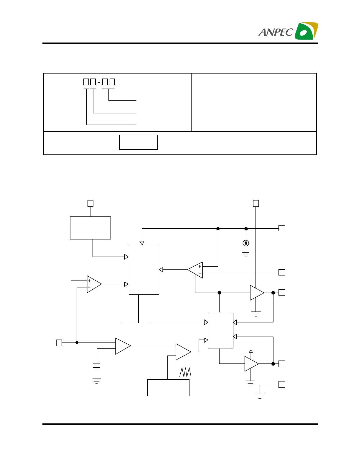
Block Diagram
VCC
UnderVoltage
Lockout
UVLO
0.5V UVP
Handling Code
Temp. Range
Package Code
APW 7057
XXXXX
Soft-Start
and Fault
Logic
Shutdown
OCP
Package Code
K : SO P -8
Operating Junction Tem p. Range
°
C : 0 to 70 C
Handling Code
TU : Tu b e
TR : Tape & Reel
XXXXX - Date Code
OC
Comparator
I
OCSET
40uA
BOOT
OCSET
PHASE
Soft-Start
FB
-
+
Error
REF
V
0.8V
Copyright ANPEC Electronics Corp.
Rev. A.3 - Oct., 2003
Amp lif ier
Inhibit
PW M
COMP
+
-
Oscillator
.ECKH/Figure 1.
OSC
F
300kHz
UGATE
Gate
Control
VCC
LGATE
GND
www.anpec.com.tw2

APW7057
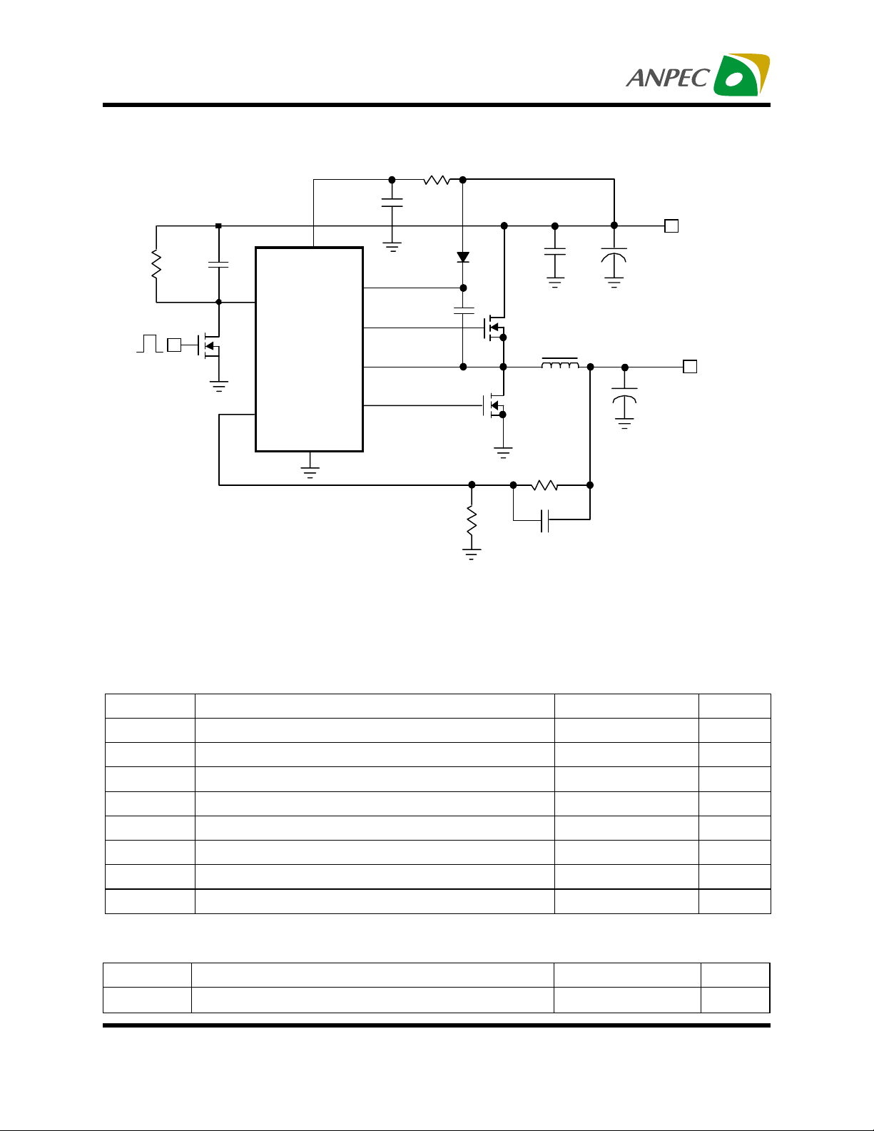
Typical Application
R3
R4
8.2k
C7
470pF
Q3
Shutdown
Q1: APM2014N U C
Q2: APM2014N U C
Q3: APM2300A A C
7
6
OCSET
APW 7057
FB
C3
1uF
5
VCC
BOOT
UGATE
PHASE
U1
LGATE
GND
3
C2: 1000uF/10V, ESR = 25m
C5: 1000uF/6.3V, ESR = 25m
1
2
8
4
1N4148
.ECKH/Figure 2.
2.2
D1
C4
0.1uF
R2
2.4k
V
IN
+
C2
1000uF x2
Q1
L1
3.3uH
C1
1uF
+
Q2
R1
5.1k
C6
0.1uF
Ω
Ω
+5V
C5
1000uF x2
V
OUT
+2.5V/10A
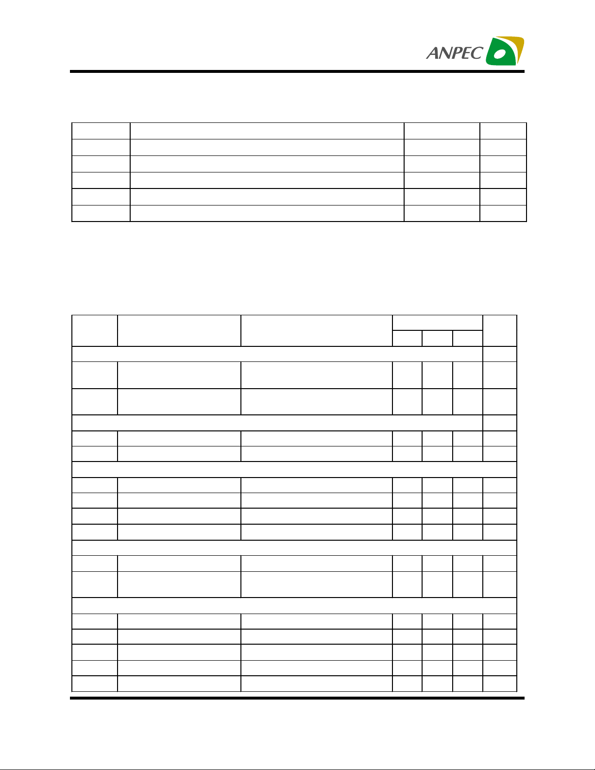
Absolute Maximum Ratings
Symbol Parameter Rating Unit
CC
V
V
BOOT
VCC Supply Voltage (VCC to GND) -0.3 ~ 7 V
BOO T S upply Voltage (BOOT to GN D ) -0.3 ~ 15 V
PHAS E , OC S ET to GND Input Voltage -0.3 ~ 12 V
FB to GN D In p u t Volta ge -0.3 ~ VCC+0.3 V
Maximum Junction Tem perature 125
STG
T
SDR
T
ESD
V
Storage Temperature -65 ~ 150
Maximum Soldering Temperature, 10 Seconds 300
Minim um ESD Rating
±2
Thermal Characteristics
Symbol Parameter Value Unit
JA
θ
Copyright ANPEC Electronics Corp.
Rev. A.3 - Oct., 2003
Junction-to-Ambient Resistance in fre e air (S OP-8) 160
www.anpec.com.tw3
o
o
o
kV
o
C/W
C
C
C

APW7057
Recommended Operating Conditions
Symbol Parameter Range Unit
VCC VCC S upply Voltage 5 ± 5% V
V
Output Voltage of the Switc hing Regulator (Note) 0.8 ~ VCC V
OUT
VIN Input Voltage of the S wit c hing Regulat or (Note) 3.3 ~ VCC V
o
C
oC
Unit
P-P
A
µ
TA Am bient Temperature 0 ~ 70
TJ Junction Temperature 0 ~ 125
Note : Refer to the typical application circuit
Electrical Characteristics
Unless otherwise specified, these specifications apply over VCC=5V, VBOOT=12V and TA= 0~70 oC. Typical
values are at TA=25oC.
Symbol Parameter Test Conditions
SUPP LY CURRENT
I
VCC
I
BOOT
VCC No mina l Supp l y
Current
BOOT Nominal Supply
Current
UGATE and LGATE Open
UGATE Open
Under Voltage Lockout(UVLO)
Risi ng V CC Threshold 4.0 4.2 4.4 V
Falli ng V CC Threshold 3.8 4.0 4.2 V
OSCILLATOR
F
Free Running Frequency 250 300 340 kHz
OSC
Ramp Upper Threshol d 2.85 V
Ramp Lower Threshol d 0.95 V
Ramp Amplitude 1.9 V
V
OSC
∆
REFERENCE VOLTAGE
V
Reference Voltage 0.8 V
REF
Referenc e Volt age
Accuracy
-1.5 +1.5 %
ERROR AMPLIFI ER
DC Gain 75 dB
FP Fi rst P ol e F requenc y 10 Hz
FZ Fi rst Zero Frequency 1 kHz
UGATE Dut y Range 0 100 %
FB Input Current
Copyright ANPEC Electronics Corp.
Rev. A.3 - Oct., 2003
APW7057
Min Typ Max
2.1 mA
2.1 mA
0.1
www.anpec.com.tw4

APW7057
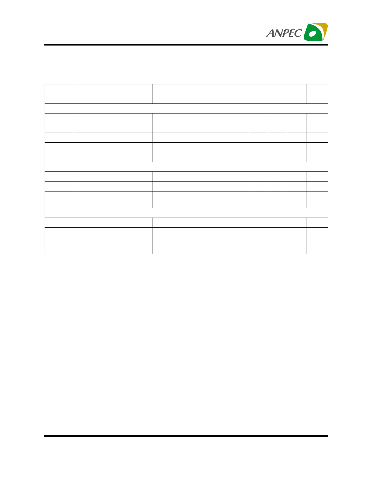
Electrical Characteristics (Cont.)
Unless otherwise specified, these specifications apply over VCC=5V, VBOOT=12V and TA= 0~70 oC. Typical
values are at TA=25oC.
Symbol Parameter Test Conditions
PWM CONTROLLER GATE DRIVERS
UGATE Source V
UGATE Sink V
LGATE Source
LGATE Sink V
D
T
Dead Time 50 nS
UAGTE
=1V 0.6 A
UGATE
=1V 7 .3
LGATE
=1V 0.6 A
V
LGATE
=1V 1.8
PROTECTIO N
OCSET
I
UV
OCSET Sink Current V
FB
FB Under-Voltage Level FB falling 0.5 V
FB Under-Voltage
Hysteresis
OCSET
=4.5V 34 40 46
15 mV
SOFT-START AND SHUTDOWN
SS
T
Soft-Start Interval 2 mS
Shutdown Threshold V
OCSET Shutdown
Hysteresis
OCSET
Falling 1.25 V
20 mV
APW7057
Unit
Min Typ Max
Ω
Ω
µA
Functional Pin Description
BOOT (Pin 1)
This pin provides the supply voltage to the high side
MOSFET driver. A voltage no greater than 13V can
be connected to this pin as a supply to the driver.
For driving logic level N-channel MOSEFT, a bootstrap circuit can be use to create a suitable driver’s
supply.
UGATE (Pin 2)
This pin provides gate drive for the high-side
MOSFET.
GND (Pin 3)
Signal and power ground for the IC. All voltage levels are measured with respect to this pin. Tie this
pin to the ground plane through the lowest impedance connection available.
Copyright ANPEC Electronics Corp.
Rev. A.3 - Oct., 2003
LGATE (Pin 4)
This pin provides the gate drive signal for the low
side MOSFET.
VCC (Pin 5)
This is the main bias supply for the controller and
its low side MOSFET driver. Must be closely
decoupled to GND (Pin 3). DO NOT apply a
voltage greater than 5.5V to this pin.
FB (Pin 6)
This pin is the inverting input of the error amplifier
and it receives the feedback voltage from an exter-
www.anpec.com.tw5
 Loading...