ANPEC APW7046BKC-TR, APW7046AKC-TU, APW7046AKC-TR, APW7046BKC-TU Datasheet

APW7046
Dual Advanced PWM and Source-Sink Linear Controller
Features
••
•
3 Regulated Voltages are provided
••
− Standard Buck Converter for VCORE
(1.15~1.50V)
− Standard Buck Converter for VMEM
(2.40~3.15V)
−Linear Controller with SOURCE-SINK Regul ation for VTT(1.25V)
••
• Simple Single-Loop Control Design
••
− Voltage-Mode PWM Control
••
• Excellent Output Voltage Regulation
••
− VCORE Output : ±1% Over Temperature
− VMEM Output : ±1.5% Over Temperature
− VTT Output : 1/2 VIN ±25mV Over Tempera ture Min. VIN = 1.7V
••
• Fast Transient Response
••
− Built-in Feedback Compensation
General Description
The APW7046 provides the power controls and protections for three output voltages on AGP/PCI Graphic Card
applications. It integrates two PWM controllers , one
SOURCE-SINK linear controller, as well as the monitor
and protection functions into a single package. One PWM
converter (PWM1) supplies the VCORE(1.5V) for the GPU
with a standard buck converter. The other standard buck
converter (PWM2) regulates the VMEM(2.5V) for the power of DDR memory. The SOURCE-SINK linear controller
control two external MOSFETs to be a linear regulator
with the capability of sourcing and sinking current. It regulates the VTT (1.25V) power for DDR T ermination voltage.
Additional built-in over-voltage protection (OVP) will be
started when the VCORE or VMEM output is above 1 15%
CORE
of each DAC setting (V
shutdown the all output voltages until re-powering on the
IC. For each PWM converter, the over-current function
monitors the output current by sensing the voltage drop
across the MOSFET‘s r
current sensing resistor.
and VMEM). OVP function will
, eliminating the need for a
DS(ON)
− Full 0% to 100% Duty Ratio
••
• Over-Voltage and Over-Current Fault Monitor
••
••
• Constant Frequency Operation(200kHz)
••
• •
• 24 pins, SOIC Package
• •
Applications
••
• M/B DDR Power Regulation
••
••
• AGP/PCI Graphics Power Regulation
••
••
• SSTL-2 Termination
••
ANPEC reserves the right to make changes to improve reliability or manufacturability without notice, and advise
customers to obtain the latest version of relevant information to verify before placing orders.
Copyright ANPEC Electronics Corp.
Rev.A.2 - Mar., 2002
Pin Description
VCC
1
UGATE1
PHASE1
SO URC E
OCSET1
SS
SD
SINK
FB
VIN
VSEN1
GND
2
3
4
5
6
7
8
9
10
11
12
24
23
22
21
20
19
18
17
16
15
14
13
www.anpec.com.tw1
BOOT
UGATE2
PHASE2
PG ND
MEM2
MEM1
MEM0
CORE2
CORE1
CORE0
OCSET2
VSEN2

APW7046
Ordering and Marking Information
APW7046
APW7046K :
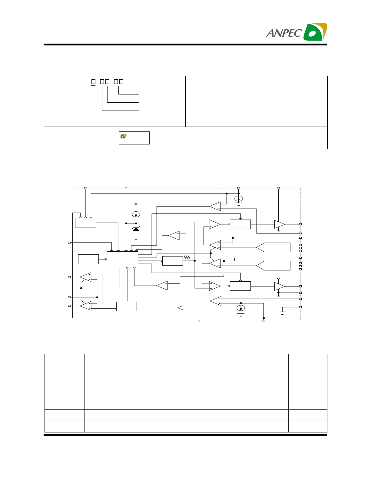
Block Diagram
VCC SS OCSET1 BOOT
Power On
Reset
SD
Therm al
Protection
SOURCE
INHIBIT
FB
SINK
50%
APW 7046
XXXXX
S oft- S tart an d
Fault Logic
Resistor
Divider
Handling Code
Tem p. Range
Package C ode
Voltage Code
VCC
28µ A
4.5V
OVP2
OVP1
O s c illa to r
115%
MEM
V
115%
Vcore
B u ffe r
Voltage Code
A : V CO RE ( 1.1 5 ~ 1 .5 0 V ) V M EM(2 .4 0 ~ 2 .75 V)
B : V CO RE ( 1.1 5 ~ 1 .5 0 V ) V M EM(2 .8 0 ~ 3 .15 V)
Package C ode
K : S OP - 24
Tem p. Range
C : 0 to 7 0
C
°
Handling Code
TU : T u b e TR : T a p e & Re e l
XXXXX - Date Code
INHIBIT
Gate
Control
INHIBIT
Gate
Control
200µ A
CORE
V
MEM
V
TTL D/A
Converter
TTL D/A
Converter
BOO T
OC1
PW M1
EA1
EA2
PW M2
OC2
200uA
UGATE1
PHASE1
VSEN1
CORE0
CORE1
CORE2
VSEN2
MEM0
MEM1
MEM2
UGATE2
PGND
PHASE2
GND
VIN
OCSET2
Absolute Maximum Ratings
Symbol Parameter Rating Unit
V
CC
VI , V
T
A
T
J
T
STG
T
S
Copyright ANPEC Electronics Corp. Rev. A.
Rev.A.2 - Mar., 2002
Supply Voltage 15 V
Input , Output or I/O V oltage GND -0.3 V to VCC +0.3 V
O
Operating Ambient Temperature Range 0 to 70
Junction Temperature Range 0 to 125
Storage Temperature Range -65 to +150
Soldering Temperature 300 ,10 seconds
www.anpec.com.tw2
C
°
C
°
C
°
C
°

APW7046
Thermal Characteristics
Symbol Parameter Value Unit
R
JA
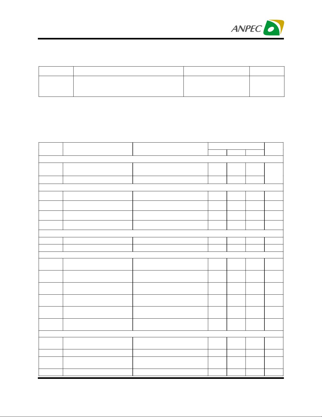
Electrical Characteristics
Unless otherwise specified, these specifications apply over VCC=VBOOT=12V and TA=0~70°C.
Typical values refer to TA=25°C.
Thermal Resistance in Free Air
SOIC
SOIC (with 3in
2
of Copper)
75
65
C/W
°
Symbol Parameter Test Conditions
Supply Current
I
I
CCSD
Nominal Supply Current
CC
Shutdown Su pply Current SD=5V 2.7
S D=0 V, UGAT E1 ,UGATE2
, SOUR C E , and SINK O p en
Power-on Reset
Rising VCC Threshold Vocset=3V 4.2 4.6 V
Fa llin g V CC Thr e s h o ld Voc s et = 3 V 3.6 V
SD In p u t H ig h Voltag e 2.0 V
SD Input Low Voltage 0.8 V
Oscillator
F
V
∆
Free Running Frequency 185 200 215 kHz
OSC
Ramp Amplitude 1.9 V
OSC
PW M Co ntroller Reference Voltage
V
CORE
PW M 1 R eference Voltage
Accuracy
COR E0-C ORE2 Input High
Voltage
COR E0-C ORE2 Input Low
Voltage
V
PW M 2 R eference Voltage
MEM
Accuracy
M E M 0 - M E M2 In p u t H ig h
Voltage
M E M 0 - M E M2 In p u t Lo w
Voltage
SOU R C E -SINK L inear Controller
V
FB Re gulation Voltage
FB
Regulator Sourcing or Sinking
Current
VFB accuracy -25 +25 mV
Max. SOURCE Pin Drive
Current
Max. SINK Pin Drive C u rrent
APW 7046
Min. Typ. Max.
8
Unit
mA
-1 +1 %
2.0 V
0.8 V
-1.5 +1.5 %
2.0 V
0.8 V
0.5VIN V
0.8
±
0.8
±
mA
mA
Copyright ANPEC Electronics Corp. Rev. A.
Rev.A.2 - Mar., 2002
www.anpec.com.tw3

APW7046
Electrical Characteristics (Cont.)
Unless otherwise specified, these specifications apply over VCC=VBOOT=12V and TA=0~70°C.
Typical values refer to TA=25°C.
Symbol Parameter Test Conditions
I
VIN Input Bias Current VIN=2.5V 2 uA
VIN
PWM Controllers Gate Drivers
I
UGATE
R
GATE
V
UGATE1,2 Source
CC=VBOOT
V
UGATE1,2
UGATE Sink VCC=12V,V
=12V,
=6V
UGATE1,2
Protection
VSEN1,2 OVP trip point
(VSEN1/V
and VSEN 2/V
CORE
MEM
VSEN Rising 115 120
)
VSEN1,2 O.V. Hysteresis 2
I
OCSET
I
Ocset Current Source Vocset=3V 170 200 230
Soft start Current 28
SS
Functional Pin Description
VCC (Pin 1)
Provide a +12V bias supply for the IC to this pin. This
pin also provides the gate bias charge for the
MOSFETs of the SOURCE-SINK regulator. The voltage at this pin is monitored for Power-On Reset (POR)
purposes.
UGA TE1 (Pin 2)
Connect this pin to the MOSFET gate of the PWM1
converter. This pin provides the gate drive for the
MOSFET.
sets the soft-start interval of all power controls and
preventing the outputs from overshoot as well as limiting the input current .
SD (Pin 5)
The pin shuts down all power outputs. A TTL compatible , logic level high signal applied at this pin immediately discharges the soft-start capacitor,disabling all
power outputs. When re-enabled, the IC undergoes a
new soft-start cycle. Left open, this pin is pulled low
by an internal pull-down resistor, enabling operation.
APW7046
Min. Typ. Max.
0.74 A
=6V 3 4
Unit
Ω
%
uA
PHASE1 (Pin 3)
Connect this pin to the PWM1 converter’s MOSFET
source.This pin is used to monitor the voltage drop
across the MOSFET for over-current protection.
SS (Pin 4)
Connect a capacitor from this pin to ground.This
capacitor, along with an internal 28uA current source,
Copyright ANPEC Electronics Corp. Rev. A.
Rev.A.2 - Mar., 2002
SOURCE (Pin 6)
Connect this pin to the upper MOSFET gate drive of
the SOURCE-SINK regulator. This pin drives the upper external MOSFET as a sourcing regulator.
SINK (Pin 7)
Connect this pin to the lower MOSFET gate drive of
www.anpec.com.tw4
 Loading...