

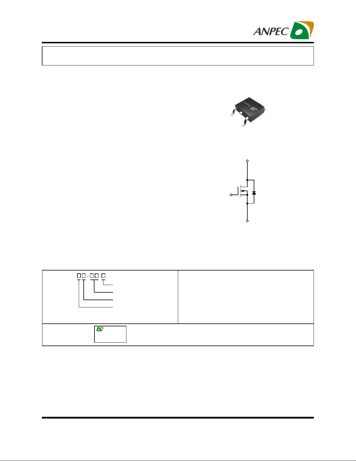
APM2505NU
N-Channel Enhancement Mode MOSFET
Fe atures
• 25V/50A,
R
R
=4mΩ (typ.) @ VGS=10V
DS(ON)
=7mΩ (typ.) @ VGS=4.5V
DS(ON)
• Super High Dense Cell Design
• Reliable and Rugged
• Lead Free Available (RoHS Compliant)
Ap plicatio ns
• Powe r Management in Desktop Computer or
DC/D C Converters
Pin De scr iption
G D
S
Top View of TO-252
D
G
S
N-C hannel MOSFET
Ord ering and Ma rking Informatio n
APM2505N
Lead Free Code
Handling Code
Temp. Range
Package Code
APM2505N U :
Note: ANPEC lead-free prod uc ts conta in molding co mp ou nds an d 10 0% matte tin plate te rmination finish ;
which are fully compliant with Ro HS and c ompatible with both SnPb and lead-free soldiering operations.
ANPEC lead-free products meet or exc eed the le ad-free re qu ire ments of IPC /J ED EC J STD-020C for MSL
classification at lead-free p eak reflow temperature.
ANPEC reserves the right to make changes to improve reliability or manufacturability without notice, and advise
customers to obtain the latest version of relevant information to verify before placing orders.
Cop yright ANPEC Electronics Corp.
Rev. B.2 - Oct., 2005
APM2505N
XXXXX
Package Code
U : TO-252
Operating Junction Temp. Range
C : -55 to 150 C
Handling Code
TU : Tube TR : Tape & Reel
Lead Free Code
L : Lead Free Device Blank : Original Device
XXXXX - Date Code
°
www.anpec.com.tw1
APM2505NU
DSS
GSS
Ab solute Maximum Ratings
Symbol
Common Ratings (T
V
V
TJ
T
STG
=25°C Unless Otherwise Noted)
A
Drain-Source Voltage
Gate-Source Voltage
Maximum Junction Temperature
Storage Temperature Range -55 to 150
IS Diode Continuous Forward Current TC=25°C
Mounted on Large Heat Sink
R
IDP
ID
PD
θ
JC
300µ s Pulse Drain Current Tested
Continuous Drain Current
Maximum Power Dissipation
Thermal Resistance-Junction to Case
Mounted on PCB of 1in2 Pad Area
IDP
300µ s Pulse Drain Current Tested
Parameter Rating Unit
25
±20
150
5
TC=25°C 120
TC=100°C 75
TC=25°C 50*
TC=100°C 30
TC=25°C
TC=100°C
50
20
2.5
TA=25°C 120
TA=100°C 75
V
°C
°C
A
A
A
W
°C/W
A
R
ID
PD
θ
JA
Continuous Drain Current
Maximum Power Dissipation
Thermal Resistance-Junction to Ambient 50 °C/W
Mounted on PCB of Minimum Footprint
IDP
ID
PD
R
θ
JA
Note:
* Current limited by bond wire.
Cop yright ANPEC Electronics Corp.
Rev. B.2 - Oct., 2005
300µ s Pulse Drain Current Tested
Continuous Drain Current
Maximum Power Dissipation
Thermal Resistance-Junction to Ambient 75 °C/W
TA=25°C 17
TA=100°C 10
TA=25°C
TA=100°C
2.5
1
TA=25°C 120
TA=100°C 75
TA=25°C 14
TA=100°C 9
TA=25°C
TA=100°C
1.6
0.6
A
W
A
A
W
www.anpec.com.tw2
APM2505NU
Electrical Characteristics (T
Symbol
Parameter Test Condition
= 25°C unless otherwise noted)
A
APM2505NU
Min. Typ. Max.
Static Characteristics
BV
Drain-Source Breakdown Voltage
DSS
VGS=0V, IDS=250µA
25 V
VDS=20V, VGS=0V 1
I
Zero Gate Voltage Drain Current
DSS
V
Gate Threshold Voltage
GS(th)
I
Gate Leakage Current VGS=±20V, VDS=0V ±100 nA
GSS
DS(ON)
a
Drain-Source On-state Resistance
R
TJ=85°C
VDS=VGS, IDS=250µA
30
1 1.5 2 V
VGS=10V, IDS=40A 4 5.5
VGS=4.5V, IDS=20A 7 8
Diode Characteristics
a
V
Diode Forward Voltage ISD=5A, VGS=0V 0.8 1.3 V
SD
Dynamic Characteristicsb
RG Gate Resistance VGS=0V,VDS=0V,F=1MHz
C
Input Capacitance 4700
iss
C
Output Capacitance 930
oss
C
Reverse Transfer Capacitance
rss
t
Turn-on Delay Time 22 41
d(ON)
Tr Turn-on Rise Time 16 29
t
Turn-off Delay Time 150 210
d(OFF)
VGS=0V,
VDS=15V,
Frequency=1.0MHz
VDD=15V, RL=15
IDS=1A, V
GEN
Ω
=10V,
,
RG=6Ω
Tf Turn-off Fall Time
1.3 Ω
280
68 82
Unit
µ
A
Ω
m
pF
ns
Gate Charge Characteristicsb
Qg Total Gate Charge 88 114
Qgs Gate-Source Charge 12.8
Qgd Gate-Drain Charge
Notes:
a : Pulse test ; pulse width≤300µs, duty cycle≤2%.
b : Guaranteed by design, not subject to production testing.
Cop yright ANPEC Electronics Corp.
Rev. B.2 - Oct., 2005
VDS=25V, VGS=10V,
IDS=30A
21.2
nC
www.anpec.com.tw3

APM2505NU
Typ ical Characteristics
Power Dissipation
60
50
40
30
Ptot - Power (W)
20
10
TC=25oC
0
0 20 40 60 80 100 120 140 160 180
Tj - Junction Temperature (°C)
Safe Operation Area
300
100
Drain Current
60
50
40
30
20
ID - Drain Current (A)
10
TC=25oC,VG=10V
0
0 20 40 60 80 100 120 140 160
Tj - Junction Temperatu re (°C)
Thermal Transient Impedance
2
1
Duty = 0.5
Rds(on) Limit
10
ID - Drain Current (A)
1
TC=25oC
0.1
0.01 0.1 1 10 100
VDS - Drain - Source Voltage (V)
Cop yright ANPEC Electronics Corp.
Rev. B.2 - Oct., 2005
10ms
100ms
1s
DC
0.2
0.1
0.01
0.01
Normalized Transient Thermal Resistance
1E-3
1E-4 1E-3 0.01 0.1 1 10 100
Square Wave Pulse Duration (sec)
0.1
0.05
0.02
Single Pulse
Mounted on 1in2 pad
R
:50oC/W
θJA
www.anpec.com.tw4

APM2505NU
Typ ical Chara cteristics (Cont.)
Output Char acteristics
120
VGS= 4,5,6,7,8,9,10V
100
80
60
40
ID - Drain Current (A)
20
0
0.0 0.2 0.4 0.6 0.8 1.0
VDS - Drain - So urce Voltage (V)
Transfer Characteristics
120
3V
Drain-Source On Resis tance
12
10
8
6
4
2
RDS(ON) - On - Resistance (mΩ)
0
0 20 40 60 80 100 120
VGS=10V
VGS=4.5V
ID - D rain Current (A)
Gate Threshold Voltage
1.4
IDS= 250µA
100
80
60
40
ID - Drain Current (A)
20
0
0 1 2 3 4 5 6
Tj=125oC
Tj=25oC
VGS - Gate - Source Voltage (V)
Cop yright ANPEC Electronics Corp.
Rev. B.2 - Oct., 2005
Tj=-55oC
1.2
1.0
0.8
0.6
Normalized Threshold Vlotage
0.4
0.2
-50 -25 0 25 50 75 100 125 150
Tj - Junction Temperature (°C)
www.anpec.com.tw5

APM2505NU
Typ ical Chara cteristics (Cont.)
Drain-Source On Resis tance
10
VGS = 10V
IDS = 40A
8
6
4
Normalized On Resistance
2
0
-50 -25 0 25 50 75 100 125 150
Tj - Junction Temperatu re (°C)
7000
RON@Tj=25oC: 4mΩ
Capacitance Gate Charge
Frequency=1MHz
6000
5000
4000
Ciss
Source-Drain Diode Forward
60
Tj=150oC
10
1
Tj=25oC
IS - Source Current (A)
0.1
0.0 0.2 0.4 0.6 0.8 1.0 1.2 1.4
VSD - Source - Drain Voltage (V)
10
VDS=15V
ID =40A
8
6
3000
2000
C - Capacitance (pF)
1000
Crss
0
0 5 10 15 20 25 30
Coss
VDS - Drain - Source Voltage (V)
Cop yright ANPEC Electronics Corp.
Rev. B.2 - Oct., 2005
4
2
VGS - Gate-source Voltage (V)
0
0 15 30 45 60 75 90
QG - Gate Charge (nC)
www.anpec.com.tw6

APM2505NU
Package Information
TO-2 52 (Reference JEDEC Registration TO-252)
E1
b
D1
E
b2
e1
A
C1
L2
D
H
L1
L
C
A1
Dim
Min. Max. Min. Max.
A 2.18 2.39 0.086 0.094
A1 0.89 1.27 0.035 0.050
b 0.508 0.89 0.020 0.035
b2 5.207 5.461 0.205 0.215
C 0.46 0.58 0.018 0.023
C1 0.46 0.58 0.018 0.023
D 5.334 6.22 0.210 0.245
D1 5.2 REF 0.205 REF
E 6.35 6.73 0.250 0.265
E1 5.3 REF 0.209 REF
e1 3.96 5.18 0.156 0.204
H 9.398 10.41 0.370 0.410
L 0.51 0.020
L1 0.64 1.02 0.025 0.040
L2 0.89 2.032 0.035 0.080
Cop yright ANPEC Electronics Corp.
Rev. B.2 - Oct., 2005
Millimeters Inches
www.anpec.com.tw7

APM2505NU
Physical Specifications
Terminal Material Solder-Plated Copper (Solder Material : 90/10 or 63/37 SnPb), 100%Sn
Lead Solderability Meets EIA Specification RSI86-91, ANSI/J-STD-002 Category 3.
Reflow Condition (IR/Convecti on or VPR Refl ow)
T
P
Ramp-up
T
L
Tsmax
Tsmin
Temperature
ts
Preheat
25
°
t 25 C to Peak
Classifi cation Reflow Profiles
tp
Ramp-down
Time
Critical Zone
TL to T
P
t
L
Profile Feature Sn-Pb Eutectic Assembly Pb-Free Assembly
Average ramp-up rate
(TL to TP)
Preheat
-
Temperature Min (Tsmin)
-
Temperature Max (Tsmax)
-
Time (min to max) (ts)
Time maintained above:
-
Temperature (TL)
-
Time (tL)
Peak/Classificatioon Temperature (Tp)
Time within 5°C of actual
Peak Temperature (tp)
Ramp-down Rate
Time 25°C to Peak Temperature
3°C/second max. 3°C/second max.
100°C
150°C
60-120 seconds
183°C
60-150 seconds
150°C
200°C
60-180 seconds
217°C
60-150 seconds
See table 1 See table 2
10-30 seconds 20-40 seconds
6°C/second max. 6°C/second max.
6 minutes max. 8 minutes max.
Notes: All temperatures refer to topside of the package .Measured on the body surface.
Cop yright ANPEC Electronics Corp.
Rev. B.2 - Oct., 2005
www.anpec.com.tw8

APM2505NU
Classifi cation Reflow Profile s(Cont.)
Table 1. SnPb Entectic Process – Package Peak Reflow Temperature s
Package Thickness Volume mm
<350
<2.5 mm
≥
2.5 mm 225 +0/-5°C 225 +0/-5°C
240 +0/-5°C 225 +0/-5°C
3
Volume mm
≥ 350
3
Table 2. Pb-free Process – Package Classification Reflow Temperatures
Package Thickness Volume mm3
<350
<1.6 mm
1.6 mm – 2.5 mm
≥
2.5 mm 250 +0°C* 245 +0°C* 245 +0°C*
*Tolerance: The device manufacturer/supplier
including the stated classification temperature (this means Peak reflow temperature +0°C.
For example 260°C+0°C) at the rated MSL level.
260 +0°C* 260 +0°C* 260 +0°C*
260 +0°C* 250 +0°C* 245 +0°C*
shall
Volume mm3
350-2000
assure process compatibility up to and
Volume mm3
>2000
Reliability Test Program
Test item Method Description
SOLDERABILITY MIL-STD-883D-2003 245°C,5 SEC
HOLT MIL-STD 883D-1005.7 1000 Hrs Bias @ 125°C
PCT JESD-22-B, A102 168 Hrs, 100% RH, 121°C
TST MIL-STD 883D-1011.9 -65°C ~ 150°C, 200 Cycles
Carrier Tape & Reel Dimensions
E
F
W
Cop yright ANPEC Electronics Corp.
Rev. B.2 - Oct., 2005
Po
P
P1
Ao
D
D1
t
Bo
Ko
www.anpec.com.tw9

APM2505NU
Application
ABCJT1T2WPE
330 ±3
100 ± 2
13 ± 0. 5
2 ± 0.5
16.4 + 0.3
-0.2
2.5± 0.5
16+ 0.3
- 0.1
8 ± 0.1
1.75± 0.1
7.5 ± 0.1
1.5 +0.1
1.5± 0.25
4.0 ± 0.1
2.0 ± 0.1
6.8 ± 0.1
10.4± 0.1
2.5± 0.1
0.3±0.05
T2
Carrier Tape & Reel Dime nsio ns (Cont.)
J
C
A
F D D1 Po P1 Ao Bo Ko tTO-252
B
T1
Cov er Tape Dimensions
Application Carrier Width Cover Tape Width Devices Per Reel
TO- 252 16 13.3 2500
Customer Service
Anpec Electronics Corp.
Head Office :
No.6, Dusing 1st Road, SBIP,
Hsin-Chu, Taiwan, R.O.C.
Tel : 886-3-5642000
Fax : 886-3-5642050
Taipei Branch :
7F, No. 137, Lane 235, Pac Chiao Rd.,
Hsin Tien City, Taipei Hsien, Taiwan, R. O. C.
Tel : 886-2-89191368
Fax : 886-2-89191369
(mm)
Cop yright ANPEC Electronics Corp.
Rev. B.2 - Oct., 2005
www.anpec.com.tw10
 Loading...