

ANPEC APL1086-VC-TU, APL1086-VC-TR, APL1086-UC-TU, APL1086-UC-TR, APL1086-GC-TU Datasheet
...
Copyright ANPEC Electronics Corp.
Rev. A.4 - Jun., 2003
APL1086
www.anpec.com.tw1
ANPEC reserves the right to make changes to improve reliability or manufacturability without notice, and advise
customers to obtain the latest version of relevant information to verify before placing orders.
1.5A Low Dropout Fast Response Positive Adjustable Regulator and Fixed
1.8V, 2.5V, 2.85V and 3.3V
••
••
•
Guaranteed Output Voltage Accuracy within 2%
••
••
•
Fast Transient Response
••
••
•
Guaranteed Dropout Voltage at Multiple
Currents
••
••
•
Load Regulation : 0.1% Typ.
••
••
•
Line Regulation : 0.03% Typ.
••
••
• Low Dropout Voltage : 1.3V Typ. at I
OUT
=1.5A
••
••
• Current Limit : 1.5A Min. at T
J
=125°C
••
••
• On-Chip Thermal Limiting : 150 °C Typ.
••
••
• Adjustable Output : 1.25~10.7V
••
••
• Standard 3-pin SOT-223, TO-252 , TO-220 and
TO-263 Power Packages.
Features
Applications
••
••
• Active SCSI Terminators
••
••
• Low Voltage Logic Supplies
••
••
• Battery-Powered Circuitry
••
••
• Post Regulator for Switching Power Supply
General Description
The APL1086 is a low dropout three-terminal adjustable regulators with 1.5A output current capability.
In order to obtain lower dropout voltage and faster
transient response, which is critical for low voltage
applications , the APL1086 has been optimized.
The device is available in an adjustable version and
fixed output voltages of 1.8V, 2.5V,2.85V and 3.3V,
the output available voltage range is from 1.25~10.
7V with an input supply below 12V. Dropout voltage
is guaranteed at a maximum of 1.45V at 1.5A.
Current limit is trimmed to ensure specified output
current and controlled short-circuit current. On-chip
thermal limiting provides protection against any combination of overload that would create excessive junction temperatures.
The APL1086 is available in the industry standard 3pin SOT-223, TO-252, TO-220 or TO-263 power
packages.
Pin Description
Front View for TO-252
TAB IS V
OUT
123
IN
OUTADJ/GND
TAB IS V
OUT
INOUTADJ/GND
123
Front View for SOT-223

Copyright ANPEC Electronics Corp.
Rev. A.4 - Jun., 2003
APL1086
www.anpec.com.tw2
Ordering and Marking Information
Symbol Parameter Rating Unit
V
I
Input Voltage 12 V
T
J
Operating Junction Temperature Range
Control Section
Power Transistor
0 to 125
0 to 150
°
C
T
STG
Storage Temperature Range -65 to +150
°
C
T
L
Lead Temperature (Soldering, 10 second) 260
°
C
Pin Description
Front View for TO-220
Front View for TO-263
1
2
3
V
IN
V
OUT
ADJ
TAB is V
OUT
1
2
3
V
IN
V
OUT
ADJ
Package Code
F : T O -22 0 G : T O -2 6 3
U : T O -2 52 V : S O T -2 23
Tem p. Range
C : 0 to 70 C
Handling Code
TU : T u b e T R : T a p e & Re e l
Voltage Code
18 : 1.8V 25 : 2.5V 285 : 2.85V 33 : 3.3V
Blank : Adjustable Version
°
APL1086-
Handling Code
Tem p. Range
Package Code
Voltage Code
APL1086
XXXXX25
XXXXX - Date Code
APL1086- 25V :
APL1086
XXXXX33
XXXXX - Date Code
APL1086- 33V :
APL1086 -33F/G/U:
APL1086
XXXXX
33
APL1086 -25F/G/U:
APL1086
XXXXX
25
APL1086 -18F/G/U:
APL1086
XXXXX
- Date Code
XXXXX
18
APL1086
XXXXX18
XXXXX - Date Code
APL1086- 18V :
APL1086
XXXXX285
XXXXX - Date Code
APL1086- 285V
:
APL1086 -285F/G/U:
APL1086
XXXXX
285
APL1086 F /G/U :
APL1086
XXXXX
XXXXX - Date CodeAPL1086 V :
- Date CodeXXXXX
- Date Code
XXXXX
- Date Code
XXXXX
APL1086
XXXXX
- Date Code
XXXXX
Absolute Maximum Ratings

Copyright ANPEC Electronics Corp.
Rev. A.4 - Jun., 2003
APL1086
www.anpec.com.tw3
Electrical Characteristics
APL1086
Symbol Parameter Test Conditions
Min. Typ. Max.
Unit
V
REF
Reference
Voltage
10mA≤ I
OUT
≤1.5A, 1.4V≤(V
IN -VOUT
)
≤9.75V,
T
J
=0~125°C
1.225 1.250 1.275 V
Output Voltage
APL1086-18
T
J
=25°C, I
OUT
=0mA,
T
J
=0~125°C,
0≤ I
OUT
≤ 1.5A, 3.5V≤VIN≤9V,
1.782
1.764
1.800
1.800
1.818
1.836
APL1086-25 T
J
=25°C, I
OUT
=0mA,
T
J
=0~125°C,
0≤ I
OUT
≤ 1.5A, 4V≤VIN≤9V,
2.475
2.450
2.500
2.500
2.525
2.550
APL1086-28 T
J
=25°C, I
OUT
=0mA,
T
J
=0~125°C,
0≤ I
OUT
≤ 1.5A, 4.25V≤VIN≤9V,
2.822
2.792
2.850
2.850
2.878
2.910
V
OUT
APL1086-33 T
J
=25°C, I
OUT
=0mA,
T
J
=0~125°C,
0≤ I
OUT
≤ 1.5A, 4.75V≤VIN≤9V,
3.267
3.235
3.300
3.300
3.333
3.365
V
Line Regulation
APL1086
T
J
=0~125°C
I
OUT
=
10mA, 1.5V≤V
IN –VOUT
≤9V, (note1)
0.03 0.2
APL1086-18
I
OUT
=
0mA, 3.5V≤V
IN
≤9V, (note1)
16
APL1086-25
I
OUT
=
0A, 4V≤V
IN
≤9V, (note 1)
16
APL1086-28
I
OUT
=
0A, 4.25V≤V
IN
≤9V, (note 1)
16
REG
LINE
APL1086-33
I
OUT
=
0A, 4.75V≤V
IN
≤ 9V, (note 1)
16
%
mV
Load Regulation
APL1086
T
J
=0~125°C
(V
IN -VOUT
)
=3V, 0≤ I
OUT
≤1.5A ,(note 1)
0.1 0.4
APL1086-18
V
IN
=3.5V, 0≤ I
OUT
≤1.5A ,(note 1)
110
APL1086-25
V
IN
=4V, 0≤ I
OUT
≤1.5A ,(note 1)
110
APL1086-28
V
IN
=4.25V, 0≤ I
OUT
≤1.5A ,(note 1)
110
REG
LOAD
APL1086-33
V
IN
=4.75V, 0≤ I
OUT
≤1.5A ,(note 1)
110
%
mV
V
D
Dropout Voltage
I
OUT
=1.5A ,T
J
=0~125°C
1.3 1.45 V
I
LIMIT
Current Limit
(V
IN -VOUT
)=5V, TJ=25°C
1500 mA
I
ADJ
Adjust Pin Current
(V
IN -VOUT
)
=3V, I
OUT
=10mA, TJ=0~125°C
60 120
µA
∆I
ADJ
Adjust Pin Current
Change
T
J
=0~125°C, 10mA≤ I
OUT
≤1.5A,
1.4V≤(V
IN -VOUT
)
≤7.75V
0.2 5
µA
I
O
Minimum Load
Current
T
J
=0~125°C, (V
IN -VOUT
)=7.75V, (note 3)
1.7 mA
PSRR Rip p le R ej ec tio n
F
RIPPLE
=120Hz, V
RIPPLE
=1V
P-P,
(V
IN -VOUT
)
=3V, TJ=0~125°C
60 75 dB
T
R
Thermal
Regulation
T
J
=25°C, 30ms Pulse
0.01 0.02 %/ W
T
S
Temper ature
Stability
0.5 %
L
S
Long -Term
Stability
T
J
=125°C,1000Hrs.
0.3 %

Copyright ANPEC Electronics Corp.
Rev. A.4 - Jun., 2003
APL1086
www.anpec.com.tw4
APL1086
Symbol Parameter Test Conditions
Min. Typ. Max.
Unit
V
N
RMS Output
Noise
T
J
=25°C,10Hz≤F≤10kH z, (% of V
OUT
)
0.003 %
θ
th
Thermal
Resistance
Junction to Case, at Tab
Junction to ambient
15
50
°C/ W
OT
Over Temperature
Point
150
°C
Quiescent Current
APL10 8 6-18
T
J
=0~125°C,
V
IN
≤9V
5.5 10
APL10 8 6-25
V
IN
≤9V
5.5 10
APL10 8 6-28
V
IN
≤9V
5.5 10
APL10 8 6-33
V
IN
≤9V
5.5 10
mA
Application Circuits
* C1 improves ripple rejection.
X
C
should be approximately
equal to R1 at ripple frequency
* Needed if device is far from filter capacitors
1.25V to 10.7V Adjustable Regulator Impro ving Ripple Rejection
R1
R2R1
1.250VV
OUT
+
×=
V
IN
10µ
F
APL1086
OUTIN
ADJ
TTL
121
Ω
365
Ω
1%
1%
+
1k
1k
100µ
F
5V
+
5V Regulator with Shutdown
V
IN
10µ
F
APL1086
OUTIN
ADJ
121
Ω
365
Ω
1%
1%
V
OUT
150µ F
10µ
F
C1
R1
R2
+
+
V
IN
10µ
F
C
1*
V
OUT1
+
R1
R2
1k
APL1086
OUTIN
ADJ
+
100µ
F
C
2
121
Ω
Note 1: See thermal regulation specifications for changes in output voltage due to heating effects. Load line regulations are measured at a constant junction temperature by low duty cycle pulse testing.
Note 2: Dropout voltage is specified over the full output current range of the device. Dropout voltage is defined as the minimum input/
output differential measured at the specified output current. Test points and limits are also shown on the Dropout Voltage curve.
Note 3: Minimum load current is defined as the minimum output current required to maintain regulation.
Electrical Characteristics (Cont.)
Copyright ANPEC Electronics Corp.
Rev. A.4 - Jun., 2003
APL1086
www.anpec.com.tw5
0.9
0.95
1
1.05
1.1
1.15
1.2
1.25
1.3
1.35
00.511.5
Dropout Voltage (V
)
0
0.5
1
1.5
2
2.5
3
3.5
4
4.5
5
-100 100 300 500 700 900
-0.03
-0.02
-0.01
0
0.01
0.02
Typical Characteristics
-20 30 80
130
180
-0.05
0
0.05
0.1
0.15
0
1
2
3
4
5
6
Dropout Voltage vs. Output Current
0
0.5
1
1.5
2
2.5
3
3.5
0123456789
Output Voltage (V)
Output Voltage vs. Input Voltage
Output Current (A) Input Voltage (V)
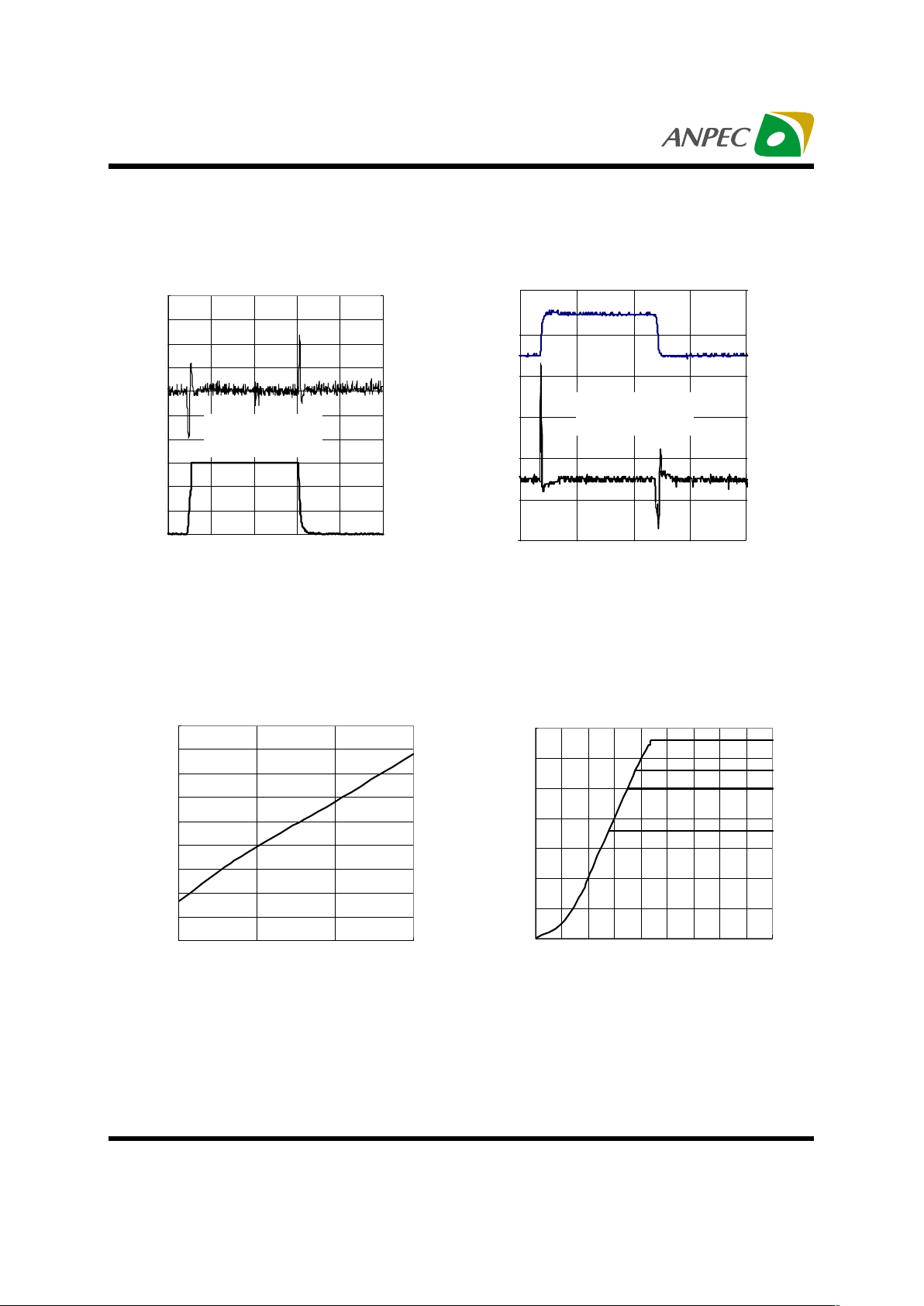
Load Transient Response
Output Current (A)
Output Voltage Deviation (V)
Time (µs)
Line Transient Response
Input Voltage (V)
Output Voltage Deviation (V)
Time (µs)
CIN=10uF
Cout=10
u
F Tantalum
V
IN
=5V
CIN=10uF
Cout=10uF Tantalum
I
OUT
=0.1A

Copyright ANPEC Electronics Corp.
Rev. A.4 - Jun., 2003
APL1086
www.anpec.com.tw6
0.9
1.4
1.9
2.4
2.9
3.4
036912
Typical Characteristics Cont.
0
1
2
3
4
5
6
0246810
Current Limit vs. Input Voltage
2.7
2.8
3.1
3.2
3.3
3.4
3.0
2.9
-50 -25 0 25 50 75 100 125
Output Voltage vs. Temperature
Output Voltage (V)
Temperature (°C)
Input Voltage (V)
Input Current vs. Input Voltage
Input Voltage (V)
Input Current (mA)
Current Limit (A)
Vout=1.25V
Output Voltage vs. Temperature
Output Voltage (V)
Temperature (°C)
1.6
1.7
1.8
1.9
2
2.1
2.2
2.3
2.4
2.5
2.6
-50 -25 0 25 50 75 100 125

Copyright ANPEC Electronics Corp.
Rev. A.4 - Jun., 2003
APL1086
www.anpec.com.tw7
Adjustable Pin Current vs. Temp erature
68
Adjustable Pin Current (
µ
A)
Temperature ( C)
°
-50 0 50 100 125-25 25 75
52
56
60
64
Typical Characteristics Cont.
Temperature ( C)
°
Input Current vs. Temperature
Input Current (mA)
2
3
4
5
6
7
8
-50 0 50 100 125-25 25 75
1.5
1.7
1.9
2.1
2.3
2.5
2.7
2.9
-5 0 -3 0 -10 10 30 50 7 0 9 0 110 130 150
Current Limit vs. Temperature
Temperature (°C)
Current Limit (mA)
Vin-Vout=5V

Copyright ANPEC Electronics Corp.
Rev. A.4 - Jun., 2003
APL1086
www.anpec.com.tw8
Package Information
SOT-223( Reference JEDEC Registration SOT-223)
B1
D
H E
K
e
e1
A
c
L
A1
a
B
b
Millimeters InchesDim
Min. Max. Min. Max.
A 1.50 1.80 0.06 0.07
A1 0.02 0.08
B 0.60 0.80 0.02 0.03
B1 2.90 3.10 0.11 0.12
c 0.28 0.32 0.01 0.01
D 6.30 6.70 0.25 0.26
E 3.30 3.70 0.13 0.15
e 2.3 BSC 0.09 BSC
e1 4.6 BSC 0.18 BSC
H 6.70 7.30 0.26 0.29
L 0.91 1.10 0.04 0.04
K 1.50 2.00 0.06 0.08
α
0
°
10
°
0
°
10
°
β
13
°
13
°

Copyright ANPEC Electronics Corp.
Rev. A.4 - Jun., 2003
APL1086
www.anpec.com.tw9
Package Informaion
TO-252( Reference JEDEC Registration TO-252)
Millimeters Inches
Dim
Min. Max. Min. Max.
A 2.18 2.39 0.086 0.094
A1 0.89 1.27 0.035 0.050
b 0.508 0.89 0.0 20 0.035
b2 5.2 07 5.461 0.205 0. 215
C 0.46 0.58 0.018 0.023
C1 0.46 0.58 0.018 0.023
D 5.334 6.22 0.2 10 0.245
D1 5.2 REF 0.205 REF
E 6.35 6.73 0.250 0.265
E1 5.3 REF 0.209 REF
e1 3.96 5.18 0.156 0.204
H 9.398 10.41 0.370 0.410
L 0.51 0.020
L1 0.64 1.02 0.025 0.040
L2 0.89 2.032 0.035 0. 080
L2
D
L1
b
b2
E
C1
A
H
L
C
A1
e1
D1
E1

Copyright ANPEC Electronics Corp.
Rev. A.4 - Jun., 2003
APL1086
www.anpec.com.tw10
Package Informaion
TO-220 ( Reference JEDEC Registration TO-220)
Q
D
R
E
F
J1
e
e1
b1
L1
A
c
b
H1
L
Millimeters Inches
Dim
Min. Max. Min. Max.
A 3.56 4.83 0.140 0.190
b1 1.14 1.78 0.045 0.070
b 0.51 1.1 4 0.020 0.04 5
c 0.31 1.14 0.01 2 0 .045
D 14.23 16.51 0.560 0.650
e 2.29 2.7 9 0.090 0.110
e1 4.83 5.33 0.190 0.210
E 9.65 10.67 0.380 0.420
F 0.51 1.40 0.020 0.055
H1 5.84 6.86 0.230 0.270
J1 2.03 2.92 0.080 0.115
L 12.7 14.73 0.500 0.580
L1 3.65 6.35 0.143 0.250
R 3.53 4.0 9 0.139 0.161
Q 2.54 3.43 0.100 0.135

Copyright ANPEC Electronics Corp.
Rev. A.4 - Jun., 2003
APL1086
www.anpec.com.tw11
Package Informaion
TO-263 ( Reference JEDEC Registration TO-263)
E
D
L
L2
L3
b2
b
e
c
A
c2
L1
Millimete rs Inches
Dim
Min. Max. Min. Max.
A 4.06 4.83 0.160 0.190
b
0.51 0.992
0.020.039
b2 1.14 1.399 0.045 0.055
c 0.38 TYP. 0.015 TYP.
c
2
1.14 1.40
0.045
0.055
D 8.64 9.65 0.340 0.380
E 9.66 10.299 0.380 0.405
e
2.543 BSC. 0.100 BSC.
L 14.60 15.88 0.575 0.625
L1 2.24 2.84
0.090
0
.11
0
L2
-2.92
-0.115
L3 1.20 1.78 0.050 0.070

Copyright ANPEC Electronics Corp.
Rev. A.4 - Jun., 2003
APL1086
www.anpec.com.tw12
Physical Specifications
Pre-heat temperature
183 C
Peak temperature
Time
°
temperature
Classification Reflow Profiles
Convection or IR/
Convection
VPR
Average ramp-up rate(183°C to Peak) 3°C/second max. 10 °C /second max.
Preheat temperature 125 ± 25°C)
120 seconds max
Temperature maintained above 183°C
60 – 150 seconds
Time within 5°C of actual peak temperature
10 –20 seconds 60 seconds
Peak temperature range
220 +5/-0°C or 235 +5/-0°C 215-219°C or 235 +5/-0°C
Ramp-down rate
6 °C /second max. 10 °C /second max.
Time 25°C to peak temperature
6 minutes max.
Package Reflow Conditions
pkg. thickness
≥≥≥≥
2.5mm
and all bgas
pkg. thickness < 2.5mm and
pkg. volume
≥≥≥≥
350 mm³
pkg. thickness < 2.5mm and pkg.
volume < 350mm³
Convection 220 +5/-0 °C Convection 235 +5/- 0 °C
VPR 215-219 °C VPR 235 +5/-0 °C
IR/Convection 220 +5/-0 °C IR/Convection 235 +5/-0 °C
Terminal Material Solder-Plated Copper (Solder Material : 90/10 or 63/37 SnPb)
Lead Solderability Meets EIA Specification RSI86-91, ANSI/J-STD-002 Category 3.
Reference JEDEC Standard J-STD-020A APRIL 1999
Reflow Condition (IR/Convection or VPR Reflow)

Copyright ANPEC Electronics Corp.
Rev. A.4 - Jun., 2003
APL1086
www.anpec.com.tw13
Rel iability tes t pr o g r am
Test item Method Description
SOLDERABILITY MIL-STD-883D-2003
245°C , 5 SEC
HOLT MIL-STD-883D-1005.7
1000 Hrs Bias @ 125 °C
PCT JESD-22-B, A102
168 Hrs, 100 % RH , 121°C
TST MIL-STD-883D-1011.9
-65°C ~ 150°C, 200 C y c les
ESD MIL-STD-883D-3015.7 VHBM > 2KV, VMM > 200V
Latch-U p JESD 78 10ms , Itr > 100mA
t
Ao
E
W
Po
P
Ko
Bo
D1
D
F
P1
Carrier Tape & Reel Dimensions
A
J
B
T2
T1
C
Applicatio n A B C J T1 T2 W P E
330 ±3 100 ± 2 13 ± 0. 5 2 ± 0.5
16.4 + 0.3
-0.2
2.5± 0.5
16+ 0.3
- 0.1
8 ± 0.1 1.75± 0.1
F D D1 Po P1 Ao Bo Ko tTO-252
7.5 ± 0.1 1.5 + 0 .1 1.5± 0.25 4.0 ± 0 .1 2.0 ± 0 .1 6.8 ± 0.1 10.4± 0 .1 2.5± 0 .1 0.3±0.05
Applicatio n A B C J T1 T2 W P E
380±3 80 ± 2 13 ± 0. 5 2 ± 0.5 24 ± 42± 0.3
24 + 0.3
- 0.1
16 ± 0.1 1.75± 0.1
F D D1 Po P1 Ao Bo Ko tTO-263
11.5 ± 0 .1 1.5 + 0.1 1.5± 0.25 4.0 ± 0 .1 2.0 ± 0.1 10.8 ± 0.1 16.1± 0.1 5 .2 ± 0.1
0.35±0.01
3
(mm)

Copyright ANPEC Electronics Corp.
Rev. A.4 - Jun., 2003
APL1086
www.anpec.com.tw14
Application Carrier Width Cover Tape Width Devices Per Reel
TO- 252
16 13.3 2500
TO- 263
24 21.3 1000
SOT- 223
12 9.3 2500
Application A B C J T1 T2 W P E
330±162±1.5
12.75±
0.15
2 ± 0.6 12.4 +0.2 2± 0.2 12 ± 0.3 8 ± 0.1 1.75± 0.1
F D D1 Po P1 Ao Bo Ko tSOT-223
5.5 ± 0.05 1.5+ 0.1 1.5+ 0.1 4.0 ± 0.1 2 .0 ± 0.05 6.9 ± 0.1 7.5± 0 .1 2.1± 0.1 0.3±0.05
(mm)
Cover Tape Dimensions
Customer Service
Anpec Electronics Corp.
Head Office :
5F, No. 2 Li-Hsin Road, SBIP,
Hsin-Chu, Taiwan, R.O.C.
Tel : 886-3-5642000
Fax : 886-3-5642050
Taipei Branch :
7F, No. 137, Lane 235, Pac Chiao Rd.,
Hsin Tien City, Taipei Hsien, Taiwan, R. O. C.
Tel : 886-2-89191368
Fax : 886-2-89191369
Reel Dimensions (Cont.)
 Loading...