

Page 1
FEATURES
LT1210
1.1A, 35MHz Current
Feedback Amplifier
U
DESCRIPTIO
■
1.1A Minimum Output Drive Current
■
35MHz Bandwidth, AV = 2, RL = 10
■
900V/µs Slew Rate, AV = 2, RL = 10
■
High Input Impedance: 10MΩ
■
Wide Supply Range: ± 5V to ±15V
Ω
Ω
(TO-220 and DD Packages)
■
Enhanced θJA SO-16 Package for ± 5V Operation
■
Shutdown Mode: IS < 200µA
■
Adjustable Supply Current
■
Stable with CL = 10,000pF
■
Available in 7-Lead DD, TO-220 and
16-Lead SO Packages
U
APPLICATIO S
■
Cable Drivers
■
Buffers
■
Test Equipment Amplifiers
■
Video Amplifiers
■
ADSL Drivers
The LT®1210 is a current feedback amplifier with high
output current and excellent large-signal characteristics.
The combination of high slew rate, 1.1A output drive and
±15V operation enables the device to deliver significant
power at frequencies in the 1MHz to 2MHz range. Shortcircuit protection and thermal shutdown ensure the
device’s ruggedness. The LT1210 is stable with large
capacitive loads, and can easily supply the large currents
required by the capacitive loading. A shutdown feature
switches the device into a high impedance and low
supply current mode, reducing dissipation when the
device is not in use. For lower bandwidth applications,
the supply current can be reduced with a single external
resistor.
The LT1210 is available in the TO-220 and DD packages
for operation with supplies up to ±15V. For ± 5V applications the device is also available in a low thermal resistance SO-16 package.
, LT, LTC and LTM are registered trademarks of Linear Technology Corporation.
All other trademarks are the property of their respective owners.
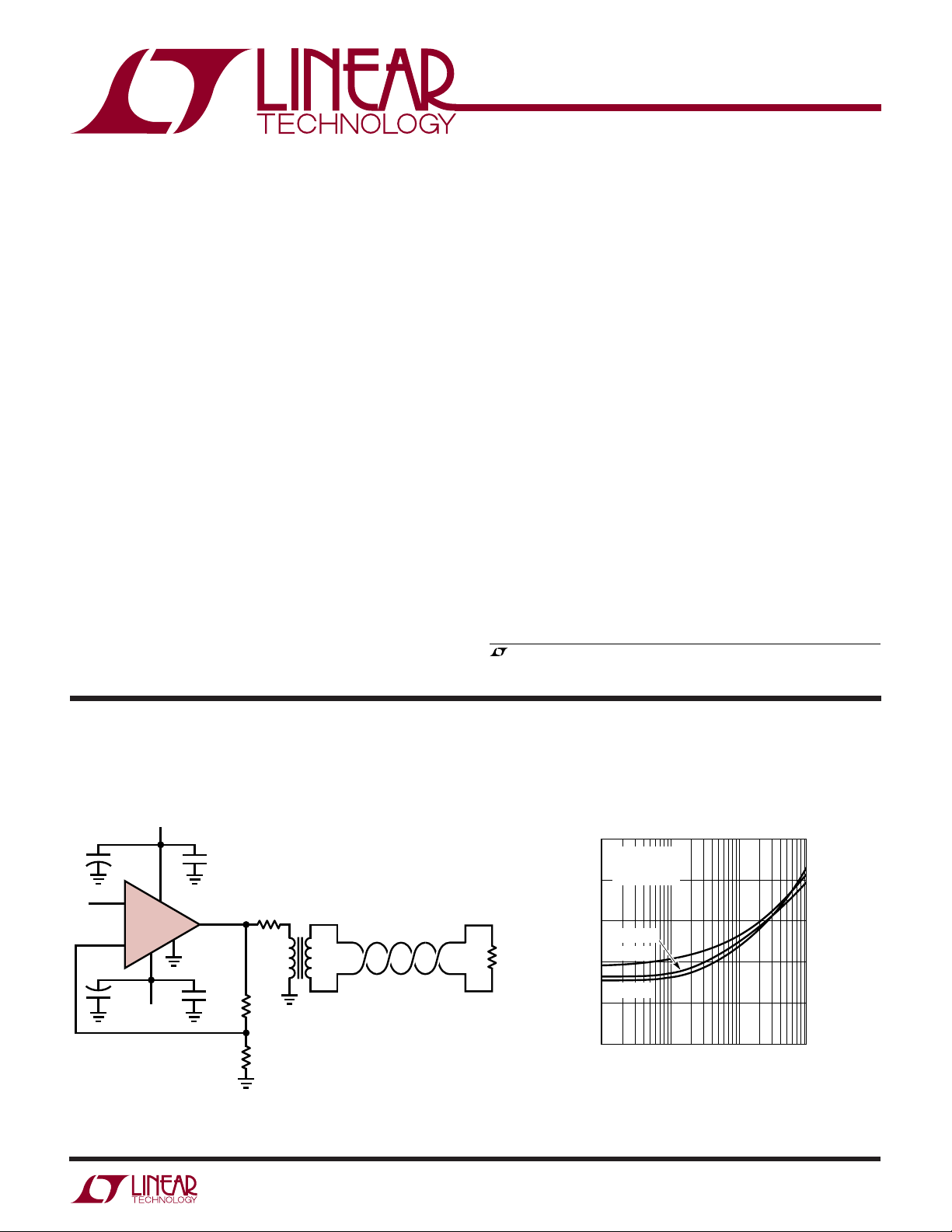
TYPICAL APPLICATIO
Twisted Pair Driver
15V
+
4.7µF*
V
IN
+
LT1210
–
4.7µF*
+
–15V
SD
100nF
100nF
R
11Ω
2.5W
845Ω
274Ω
T
U
T1**
31
* TANTALUM
** MIDCOM 671-7783 OR EQUIVALENT
R
100Ω
2.5W
1210 TA01
Total Harmonic Distortion vs Frequency
–50
VS = ±15V
= 20V
V
OUT
AV = 4
–60
–70
L
RL = 12.5Ω
RL = 10Ω
–80
RL = 50Ω
–90
TOTAL HARMONIC DISTORTION (dB)
–100
1k
P-P
10k 100k 1M
FREQUENCY (Hz)
1210 TA02
1210fa
1
Page 2
LT1210
A
W
O
LUTEXI TIS
S
A
WUW
U
(Note 1)
ARB
G
Supply Voltage ..................................................... ± 18V
Input Current .................................................... ±15mA
Output Short-Circuit Duration (Note 2) ....... Continuous
Specified Temperature Range (Note 3) ...... 0°C to 70°C
U
W
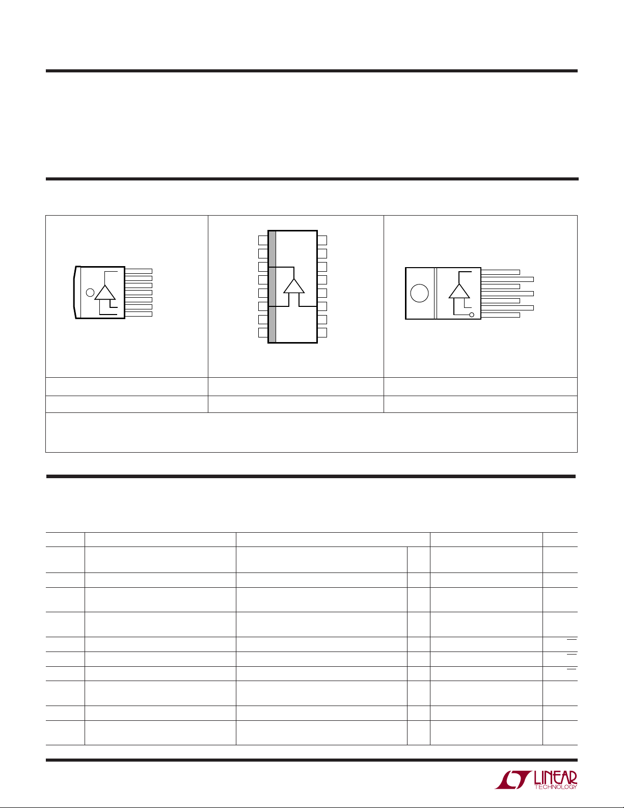
PACKAGE/ORDER INFORMATION
TOP VIEW
+
1
V
+
2
FRONT VIEW
7
6
5
4
TAB
IS V
3
2
+
1
R PACKAGE
7-LEAD PLASTIC DD
θJA ≈ 25°C/W
OUT
–
V
COMP
+
V
SHUTDOWN
+IN
–IN
V
3
OUT
+
4
V
5
NC
6
–IN
7
NC
+
8
V
16-LEAD PLASTIC SO
θJA ≈ 40°C/W (Note 3)
S PACKAGE
Operating Temperature Range ............... –40°C to 85°C
Junction Temperature......................................... 150°C
Storage Temperature Range ................. –65°C to 150°C
Lead Temperature (Soldering, 10 sec)................. 300°C
U
+
16
V
15
NC
14
V
13
COMP
12
SHUTDOWN
11
+IN
10
NC
9
V
–
+
TAB
IS V
FRONT VIEW
+
T7 PACKAGE
7-LEAD TO-220
7
6
5
4
3
2
1
θJC = 5°C/W
OUT
–
V
COMP
+
V
SHUTDOWN
+IN
–IN
ORDER PART NUMBER ORDER PART NUMBER
LT1210CR
ORDER PART NUMBER
LT1210CS
LT1210CT7
Order Options Tape and Reel: Add #TR
Lead Free: Add #PBF Lead Free Tape and Reel: Add #TRPBF
Lead Free Part Marking: http://www.linear.com/leadfree/
Consult LTC Marketing for parts specified with wider operating temperature ranges.
ELECTRICAL CHARACTERISTICS
temperature range, otherwise specifications are at T
The ● denotes specifications which apply over the full operating
= 25°C. VCM = 0V, ± 5V ≤ VS ≤ ± 15V, pulse tested, VSD = 0V, unless
A
otherwise noted.
SYMBOL PARAMETER CONDITIONS MIN TYP MAX UNITS
V
I
I
e
+i
–i
R
C
OS
+
IN
–
IN
n
n
n
IN
IN
Input Offset Voltage TA = 25°C ±3 ±15 mV
Input Offset Voltage Drift
●
●
10 µV/°C
± 20 mV
Noninverting Input Current TA = 25°C ±2 ±5 µA
●
± 20 µA
Inverting Input Current TA = 25°C ±10 ± 60 µA
●
±100 µA
Input Noise Voltage Density f = 10kHz, RF = 1k, RG = 10Ω, RS = 0Ω 3.0 nV/√Hz
Input Noise Current Density f = 10kHz, RF = 1k, RG = 10Ω, RS = 10k 2.0 pA/√Hz
Input Noise Current Density f = 10kHz, RF = 1k, RG = 10Ω, RS = 10k 40 pA/√Hz
Input Resistance VIN = ±12V, VS = ± 15V
VIN = ±2V, VS = ±5V
●
1.50 10 MΩ
●
0.25 5 MΩ
Input Capacitance VS = ± 15V 2 pF
Input Voltage Range VS = ± 15V
= ± 5V
V
S
●
±12 ± 13.5 V
●
±2 ±3.5 V
1210fa
2
Page 3

LT1210
ELECTRICAL CHARACTERISTICS
temperature range, otherwise specifications are at T
The ● denotes specifications which apply over the full operating
= 25°C. VCM = 0V, ± 5V ≤ VS ≤ ± 15V, pulse tested, VSD = 0V, unless
A
otherwise noted.
SYMBOL PARAMETER CONDITIONS MIN TYP MAX UNITS
CMRR Common Mode Rejection Ratio VS = ± 15V, VCM = ± 12V
= ± 5V, VCM = ±2V
V
S
Inverting Input Current VS = ± 15V, VCM = ± 12V
Common Mode Rejection V
= ± 5V, VCM = ±2V
S
PSRR Power Supply Rejection Ratio VS = ± 5V to ±15V
Noninverting Input Current VS = ± 5V to ±15V
Power Supply Rejection
Inverting Input Current VS = ± 5V to ±15V
Power Supply Rejection
A
V
R
OL
V
OUT
Large-Signal Voltage Gain TA = 25°C, VS = ±15V, V
R
= 10Ω (Note 3)
L
Transresistance, ∆V
OUT
/∆I
VS = ± 15V, V
VS = ± 5V, V
–
IN
TA = 25°C, VS = ±15V, V
R
= 10Ω (Note 3) 100 260 kΩ
L
VS = ± 15V, V
VS = ± 5V, V
= ±8.5V, RL = 10Ω (Note 3)
OUT
= ± 2V, RL = 10Ω
OUT
= ±8.5V, RL = 10Ω (Note 3)
OUT
= ± 2V, RL = 10Ω
OUT
= ± 10V, 55 71 dB
OUT
= ± 10V,
OUT
Maximum Output Voltage Swing TA = 25°C, VS = ±15V, RL = 10Ω (Note 3) ±10.0 ± 11.5 V
TA = 25°C, VS = ±5V, RL = 10Ω ± 2.5 ± 3.0 V
I
I
OUT
S
Maximum Output Current (Note 4) VS = ± 15V, RL = 1Ω
Supply Current (Note 4) TA = 25°C, VS = ± 15V, VSD = 0V 35 50 mA
Supply Current, RSD = 51k (Notes 4, 5) TA = 25°C, VS = ± 15V 15 30 mA
Positive Supply Current, Shutdown VS = ± 15V, VSD = 15V
Output Leakage Current, Shutdown VS = ± 15V, VSD = 15V
SR Slew Rate (Note 6) TA = 25°C, AV = 2, RL = 400Ω 400 900 V/µs
Slew Rate (Note 4) T
= 25°C, AV = 2, RL = 10Ω 900 V/µs
A
Differential Gain (Notes 4, 7) VS = ± 15V, RF = 750Ω, RG = 750Ω, RL = 15Ω 0.3 %
Differential Phase (Notes 4, 7) VS = ± 15V, RF = 750Ω, RG = 750Ω, RL = 15Ω 0.1 DEG
BW Small-Signal Bandwidth AV = 2, VS = ± 15V, Peaking ≤ 1dB, 55 MHz
= RG = 680Ω, RL = 100Ω
R
F
AV = 2, VS = ± 15V, Peaking ≤ 1dB, 35 MHz
= RG = 576Ω, RL = 10Ω
R
F
●
55 62 dB
●
50 60 dB
●
●
●
60 77 dB
●
●
●
55 68 dB
●
55 68 dB
●
75 200 kΩ
●
75 200 kΩ
●
± 8.5 V
●
± 2.0 V
●
1.1 2.0 A
●
●
●
0.1 10 µA/V
0.1 10 µA/V
30 500 nA/V
0.7 5 µA/V
65 mA
200 µA
10 µA
Note 1: Stresses beyond those listed under Absolute Maximum Ratings
may cause permanent damage to the device. Exposure to any Absolute
Maximum Rating condition for extended periods may affect device
reliability and lifetime.
Note 2: Applies to short circuits to ground only. A short circuit between
the output and either supply may permanently damage the part when
operated on supplies greater than ±10V.
Note 3: Commercial grade parts are designed to operate over the
temperature range of – 40°C ≤ T
guaranteed beyond 0°C ≤ T
–40°C ≤ T
≤ 85°C are available on special request. Consult factory.
A
≤ 85°C, but are neither tested nor
A
≤ 70°C. Industrial grade parts tested over
A
Note 4: SO package is recommended for ±5V supplies only, as the power
dissipation of the SO package limits performance on higher supplies. For
supply voltages greater than ±5V, use the TO-220 or DD package. See
“Thermal Considerations” in the Applications Information section for
details on calculating junction temperature. If the maximum dissipation of
the package is exceeded, the device will go into thermal shutdown.
Note 5: R
is connected between the Shutdown pin and ground.
SD
Note 6: Slew rate is measured at ±5V on a ± 10V output signal while
operating on ±15V supplies with R
= 1.5k, RG = 1.5k and RL = 400Ω.
F
Note 7: NTSC composite video with an output level of 2V.
1210fa
3
Page 4

LT1210
W
UU
SMALL-SIGNAL BANDWIDTH
RSD = 0Ω, IS = 30mA, VS = ± 5V, Peaking ≤ 1dB
A
V
– 1 150 549 549 52.5
1 150 604 – 53.5
2 150 562 562 51.8
10 150 392 43.2 48.4
RSD = 7.5k, IS = 15mA, VS = ± 5V, Peaking ≤ 1dB
A
V
– 1 150 562 562 39.7
1 150 634 – 41.9
2 150 576 576 40.2
10 150 324 35.7 39.5
R
L
30 590 590 39.7
10 619 619 26.5
30 649 – 39.7
10 619 – 27.4
30 590 590 38.8
10 576 576 27.4
30 383 42.2 40.3
10 215 23.7 36.0
R
L
30 619 619 28.9
10 604 604 20.5
30 681 – 29.7
10 649 – 20.7
30 604 604 29.6
10 576 576 21.6
30 324 35.7 32.3
10 210 23.2 27.7
R
F
R
F
R
G
R
G
–3dB BW
(MHz)
–3dB BW
(MHz)
RSD = 0Ω, IS = 35mA, VS = ± 15V, Peaking ≤ 1dB
A
V
– 1 150 604 604 66.2
1 150 750 – 56.8
2 150 665 665 52.5
10 150 453 49.9 61.5
R
L
30 649 649 48.4
10 665 665 46.5
30 866 – 35.4
10 845 – 24.7
30 715 715 38.9
10 576 576 35.0
30 432 47.5 43.1
10 221 24.3 45.5
R
F
R
G
RSD = 47.5k, IS = 18mA, VS = ± 15V, Peaking ≤ 1dB
A
V
– 1 150 619 619 47.8
1 150 732 – 51.4
2 150 634 634 48.4
10 150 348 38.3 46.8
R
L
30 698 698 32.3
10 698 698 22.2
30 806 – 33.9
10 768 – 22.5
30 698 698 33.0
10 681 681 22.5
30 357 39.2 36.7
10 205 22.6 31.3
R
F
R
G
–3dB BW
(MHz)
–3dB BW
(MHz)
RSD = 15k, IS = 7.5mA, VS = ± 5V, Peaking ≤ 1dB
A
V
– 1 150 536 536 28.2
1 150 619 – 28.6
2 150 536 536 28.3
10 150 150 16.5 31.5
R
L
30 549 549 20.0
10 464 464 15.0
30 634 – 19.8
10 511 – 14.9
30 549 549 19.9
10 412 412 15.7
30 118 13.0 27.1
10 100 11.0 19.4
R
F
R
G
4
–3dB BW
(MHz)
RSD = 82.5k, IS = 9mA, VS = ± 15V, Peaking ≤ 1dB
A
V
– 1 150 590 590 34.8
1 150 715 – 35.5
2 150 590 590 35.3
10 150 182 20.0 37.2
R
L
30 649 649 22.5
10 576 576 16.3
30 768 – 22.5
10 649 – 16.1
30 665 665 22.5
10 549 549 16.8
30 182 20.0 28.9
10 100 11.0 22.5
R
F
R
G
–3dB BW
(MHz)
1210fa
Page 5
WU
CAPACITIVE LOAD (pF)
100
FEEDBACK RESISTANCE (Ω)
1k
10k
100101 10000
1210 G03
1000
BANDWIDTH
FEEDBACK RESISTANCE
A
V
= 2
R
L
=
∞
VS = ±15V
C
COMP
= 0.01µF
1
10
100
–3dB BANDWIDTH (MHz)
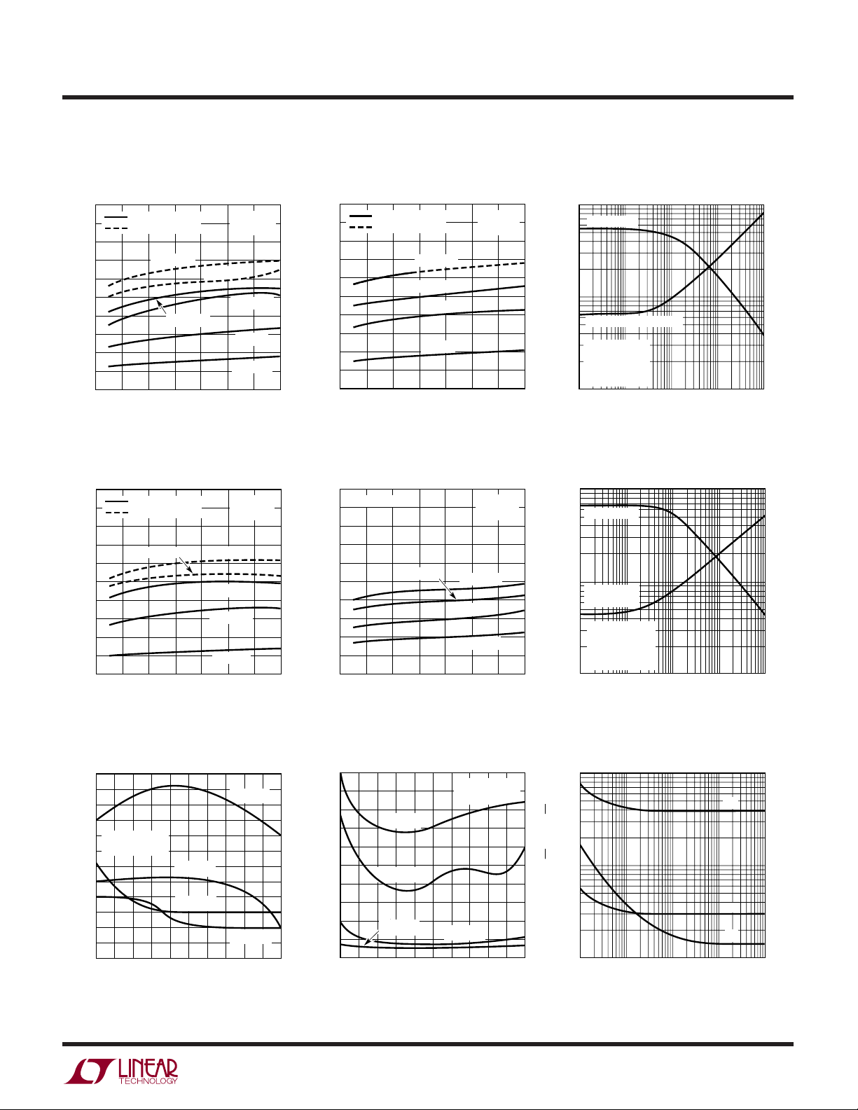
TYPICAL PERFOR A CE CHARACTERISTICS
Bandwidth vs Supply Voltage
100
90
80
70
60
50
40
30
– 3dB BANDWIDTH (MHz)
20
10
0
PEAKING ≤ 1dB
PEAKING ≤ 5dB
RF = 470Ω
4
610
8
SUPPLY VOLTAGE (±V)
RF = 680Ω
12
Bandwidth vs Supply Voltage
100
90
80
70
60
50
40
30
–3dB BANDWIDTH (MHz)
20
10
0
PEAKING ≤ 1dB
PEAKING ≤ 5dB
RF =390Ω
4
610
8
SUPPLY VOLTAGE (±V)
12
AV = 2
R
RF = 560Ω
RF = 750Ω
RF = 1.5k
14
AV = 10
R
RF = 330Ω
RF = 470Ω
RF = 680Ω
RF = 1.5k
14
= 100Ω
L
RF = 1k
16
= 100Ω
L
16
1210 G04
18
1210 G01
18
Bandwidth vs Supply Voltage
50
40
30
20
–3dB BANDWIDTH (MHz)
10
0
PEAKING ≤ 1dB
PEAKING ≤ 5dB
4
610
8
SUPPLY VOLTAGE (±V)
RF = 560Ω
RF = 750Ω
RF = 1k
RF = 2k
12
Bandwidth vs Supply Voltage
50
PEAKING ≤ 1dB
40
30
20
– 3dB BANDWIDTH (MHz)
10
0
4
RF = 680Ω
610
8
SUPPLY VOLTAGE (±V)
12
AV = 2
R
L
14
AV = 10
= 10Ω
R
L
RF = 560Ω
RF = 1k
RF = 1.5k
14
= 10Ω
16
1210 G02
16
1210 G05
LT1210
Bandwidth and Feedback Resistance
vs Capacitive Load for Peaking ≤ 1dB
18
Bandwidth and Feedback Resistance
vs Capacitive Load for Peaking ≤ 5dB
10k
BANDWIDTH
1k
FEEDBACK
RESISTANCE
AV = +2
FEEDBACK RESISTANCE (Ω)
=
∞
R
L
VS = ±15V
= 0.01µF
C
COMP
0100
0
18
1
10 100 1000 10000
CAPACITIVE LOAD (pF)
100
–3dB BANDWIDTH (MHz)
10
1
1210 G06
Differential Phase vs
Supply Voltage
0.6
0.5
0.4
RF = RG = 750Ω
= 2
A
V
0.3
0.2
DIFFERENTIAL PHASE (DEG)
0.1
0
7
5
9
SUPPLY VOLTAGE (±V)
RL = 15Ω
RL = 50Ω
RL = 10Ω
RL = 30Ω
11
13
1210 G07
0.5
0.4
0.3
0.2
DIFFERENTIAL GAIN (%)
0.1
15
Differential Gain vs
Supply Voltage
RL = 10Ω
RL = 15Ω
RL = 50Ω
0
7
5
9
SUPPLY VOLTAGE (±V)
RF = RG = 750Ω
= 2
A
V
RL = 30Ω
11
13
1210 G08
Spot Noise Voltage and Current
vs Frequency
100
–i
n
10
e
n
SPOT NOISE (nV/√Hz OR pA/√Hz)
15
1
10
100 100k
1k 10k
FREQUENCY (Hz)
+i
n
1210 G09
1210fa
5
Page 6

LT1210
WU
TYPICAL PERFOR A CE CHARACTERISTICS
Supply Current vs Supply Voltage
40
RSD = 0Ω
38
36
34
32
30
28
26
SUPPLY CURRENT (mA)
24
22
20
4
610
TA = 25°C
TA = 85°C
TA = 125°C
8
SUPPLY VOLTAGE (±V)
12
Supply Current vs
Shutdown Pin Current
40
VS = ±15V
35
30
25
20
15
SUPPLY CURRENT (mA)
10
5
0
100
0
SHUTDOWN PIN CURRENT (µA)
200
300
TA = –40°C
14
400
16
1210 G10
1210 G13
18
500
Supply Current vs
Ambient Temperature, VS = ± 5V
40
35
30
25
20
15
SUPPLY CURRENT (mA)
10
5
0
–50
–25
0
RSD = 0Ω
RSD = 7.5k
= 15k
R
SD
50
25
TEMPERATURE (°C)
Input Common Mode Limit vs
Junction Temperature
+
V
– 0.5
–1.0
–1.5
–2.0
2.0
1.5
1.0
COMMON MODE RANGE (V)
0.5
–
V
–25 100
–50
0 125
TEMPERATURE (°C)
50
25
Supply Current vs
Ambient Temperature, VS = ±15V
AV = 1
=
∞
R
L
100
125
1210 G11
75
40
35
30
25
20
15
SUPPLY CURRENT (mA)
10
5
0
–50
–25
0
TEMPERATURE (°C)
RSD = 0Ω
RSD = 47.5k
RSD = 82.5k
50
25
AV = 1
=
∞
R
L
100
125
1210 G12
75
Output Short-Circuit Current vs
Junction Temperature
3.0
2.8
2.6
2.4
2.2
2.0
1.8
OUTPUT SHORT-CIRCUIT CURRENT (A)
1.6
–50
75
1210 G14
–25 0
SOURCING
SINKING
50 100 125
25 75
TEMPERATURE (°C)
1210 G15
Output Saturation Voltage vs
Junction Temperature
+
V
VS = ±15V
–1
–2
–3
–4
4
3
2
OUTPUT SATURATION VOLTAGE (V)
1
–
V
–50
0 125
–25 100
25
TEMPERATURE (°C)
6
RL = 10Ω
RL = 10Ω
50
RL = 2k
RL = 2k
75
1210 G16
Power Supply Rejection Ratio
vs Frequency
70
60
NEGATIVE
50
POSITIVE
40
30
20
POWER SUPPLY REJECTION (dB)
10
0
10k 1M 10M 100M
100k
FREQUENCY (Hz)
RL = 50Ω
= ±15V
V
S
= RG = 1k
R
F
1210 G17
Supply Current vs Large-Signal
Output Frequency (No Load)
100
AV = 2
=
∞
R
90
L
VS = ±15V
= 20V
V
OUT
80
70
60
50
SUPPLY CURRENT (mA)
40
30
20
10k
P-P
100k 1M 10M
FREQUENCY (Hz)
1210 G18
1210fa
Page 7

WU
TYPICAL PERFOR A CE CHARACTERISTICS
LT1210
Output Impedance vs Frequency
100
VS = ±15V
= 0mA
I
O
10
RSD = 82.5k
1
0.1
OUTPUT IMPEDANCE (Ω)
0.01
100k 10M 100M
1M
FREQUENCY (Hz)
RSD = 0Ω
3rd Order Intercept vs Frequency Test Circuit for 3rd Order Intercept
56
54
52
50
48
46
44
3RD ORDER INTERCEPT (dBm)
42
40
0
2
FREQUENCY (MHz)
Output Impedance in Shutdown
vs Frequency
10k
1k
100
10
OUTPUT IMPEDANCE (Ω)
1
100k 10M 100M
1210 G19
VS = ±15V
= 10Ω
R
L
= 680Ω
R
F
= 220Ω
R
G
468
1210 G22
10
1M
FREQUENCY (Hz)
LARGE-SIGNAL VOLTAGE GAIN (dB)
1210 G20
+
LT1210
–
680Ω
220Ω
MEASURE INTERCEPT AT P
Large-Signal Voltage Gain vs
Frequency
18
AV = 4, RL = 10Ω
= 680Ω, RG = 220Ω
R
F
15
V
= ±15V, VIN = 5V
S
12
9
6
3
0
3
4
10
10
10Ω
O
1210 TC01
P-P
5
10
FREQUENCY (Hz)
P
O
10
6
7
1210 G21
8
10
10
1210fa
7
Page 8

LT1210
PPLICATI
A
U
O
S
I FOR ATIO
WU
U
The LT1210 is a current feedback amplifier with high
output current drive capability. The device is stable with
large capacitive loads and can easily supply the high
currents required by capacitive loads. The amplifier will
drive low impedance loads such as cables with excellent
linearity at high frequencies.
Feedback Resistor Selection
The optimum value for the feedback resistors is a function
of the operating conditions of the device, the load impedance and the desired flatness of response. The Typical AC
Performance tables give the values which result in less
than 1dB of peaking for various resistive loads and operating conditions. If this level of flatness is not required, a
higher bandwidth can be obtained by use of a lower
feedback resistor. The characteristic curves of Bandwidth
vs Supply Voltage indicate feedback resistors for peaking
up to 5dB. These curves use a solid line when the response
has less than 1dB of peaking and a dashed line when the
response has 1dB to 5dB of peaking. The curves stop
where the response has more than 5dB of peaking.
For resistive loads, the COMP pin should be left open (see
Capacitive Loads section).
14
VS = ±15V
12
= 200pF
C
L
10
8
COMPENSATION
6
4
2
0
VOLTAGE GAIN (dB)
–2
–4
–6
1
NO COMPENSATION
RF = 1.5k
FREQUENCY (MHz)
RF = 3.4k
= 3.4k
R
F
COMPENSATION
10 100
Figure 1
1210 F01
tance. Also shown is the –3dB bandwidth with the suggested feedback resistor vs the load capacitance.
Although the optional compensation works well with
capacitive loads, it simply reduces the bandwidth when it
is connected with resistive loads. For instance, with a 10Ω
load, the bandwidth drops from 35MHz to 26MHz when
the compensation is connected. Hence, the compensation
was made optional. To disconnect the optional compensation, leave the COMP pin open.
Capacitive Loads
The LT1210 includes an optional compensation network
for driving capacitive loads. This network eliminates most
of the output stage peaking associated with capacitive
loads, allowing the frequency response to be flattened.
Figure 1 shows the effect of the network on a 200pF load.
Without the optional compensation, there is a 6dB peak at
40MHz caused by the effect of the capacitance on the
output stage. Adding a 0.01µF bypass capacitor between
the output and the COMP pins connects the compensation
and greatly reduces the peaking. A lower value feedback
resistor can now be used, resulting in a response which is
flat to ± 1dB to 40MHz. The network has the greatest effect
in the range of 0pF to 1000pF. The graphs of
for C
L
Bandwidth and Feedback Resistance vs Capacitive Load
can be used to select the appropriate value of feedback
resistor. The values shown are for 1dB and 5dB peaking at
a gain of 2 with no resistive load. This is a worst-case
condition, as the amplifier is more stable at higher gains
and with some resistive load in parallel with the capaci-
Shutdown/Current Set
If the shutdown feature is not used, the SHUTDOWN pin
–
must be connected to ground or V
.
The Shutdown pin can be used to either turn off the biasing
for the amplifier, reducing the quiescent current to less
than 200µA, or to control the quiescent current in normal
operation.
The total bias current in the LT1210 is controlled by the
current flowing out of the Shutdown pin. When the Shutdown pin is open or driven to the positive supply, the part
is shut down. In the shutdown mode, the output looks like
a 70pF capacitor and the supply current is typically less
than 100µA. The Shutdown pin is referenced to the posi-
tive supply through an internal bias circuit (see the Simplified Schematic). An easy way to force shutdown is to use
open-drain (collector) logic. The circuit shown in Figure 2
uses a 74C904 buffer to interface between 5V logic and the
LT1210. The switching time between the active and shutdown states is about 1µs.
A 24k pull-up resistor speeds
1210fa
8
Page 9

LT1210
PPLICATI
A
ENABLE
V
IN
5V
U
O
S
I FOR ATIO
15V
+
LT1210
SD
–
–15V
74C906
24k
WU
V
OUT
R
F
R
15V
G
1210 F02
U
Figure 2. Shutdown Interface
up the turn-off time and ensures that the LT1210 is
completely turned off. Because the pin is referenced to
the positive supply, the logic used should have a breakdown voltage of greater than the positive supply voltage.
No other circuitry is necessary as the internal circuit
limits the Shutdown pin current to about 500µA. Figure
3 shows the resulting waveforms.
response. The quiescent current can be reduced to 9mA in
the inverting configuration without much change in response. In noninverting mode, however, the slew rate is
reduced as the quiescent current is reduced.
RF = 750Ω
= 10Ω
R
L
= 9mA, 18mA, 36mA
I
Q
= ±15V
V
S
Figure 4a. Large-Signal Response vs IQ, AV = –1
1210 F04a
OUT
V
ENABLE
AV = 1
= 825Ω
R
F
R
= 50Ω
L
R
PULL-UP
V
= 1V
IN
VS = ±15V
= 24k
P-P
1210 F03
Figure 3. Shutdown Operation
For applications where the full bandwidth of the amplifier
is not required, the quiescent current of the device may be
reduced by connecting a resistor from the Shutdown pin
to ground. The quiescent current will be approximately 65
times the current in the Shutdown pin. The voltage across
the resistor in this condition is V
+
– 3VBE. For example, a
82k resistor will set the quiescent supply current to 9mA
with V
= ±15V.
S
The photos in Figures 4a and 4b show the effect of
reducing the quiescent supply current on the large-signal
RF = 750Ω
R
= 10Ω
L
IQ = 9mA, 18mA, 36mA
= ±15V
V
S
1210 F04b
Figure 4b. Large-Signal Response vs IQ, AV = 2
Slew Rate
Unlike a traditional op amp, the slew rate of a current
feedback amplifier is not independent of the amplifier gain
configuration. There are slew rate limitations in both the
input stage and the output stage. In the inverting mode,
and for higher gains in the noninverting mode, the signal
amplitude on the input pins is small and the overall slew
rate is that of the output stage. The input stage slew rate
is related to the quiescent current and will be reduced as
the supply current is reduced. The output slew rate is set
by the value of the feedback resistors and the internal
capacitance. Larger feedback resistors will reduce the
slew rate as will lower supply voltages, similar to the way
1210fa
9
Page 10

LT1210
PPLICATI
A
U
O
S
I FOR ATIO
WU
U
the bandwidth is reduced. The photos in Figures 5a, 5b and
5c show the large-signal response of the LT1210 for
various gain configurations. The slew rate varies from
770V/µs for a gain of 1, to 1100V/µs for a gain of –1.
RF = 825Ω
R
= 10Ω
L
Figure 5a. Large-Signal Response, A
V
S
= ±15V
1210 F05a
= 1
V
When the LT1210 is used to drive capacitive loads, the
available output current can limit the overall slew rate. In
the fastest configuration, the LT1210 is capable of a slew
rate of over 1V/ns. The current required to slew a capacitor
at this rate is 1mA per picofarad of capacitance, so
10,000pF would require 10A! The photo (Figure 6) shows
the large-signal behavior with CL = 10,000pF. The slew
rate is about 150V/µs, determined by the current limit of
1.5A.
RF = RG = 750Ω
R
= 10Ω
L
Figure 5b. Large-Signal Response, AV = –1
RF = RG = 750Ω
R
= 10Ω
L
Figure 5c. Large-Signal Response, AV = 2
V
= ±15V
S
VS = ±15V
1210 F05b
1210 F05c
RF = RG = 3k
=
∞
R
L
Figure 6. Large-Signal Response, C
VS = ±15V
1210 F06
= 10,000pF
L
Differential Input Signal Swing
The differential input swing is limited to about ±6V by an
ESD protection device connected between the inputs. In
normal operation, the differential voltage between the
input pins is small, so this clamp has no effect; however,
in the shutdown mode the differential swing can be the
same as the input swing. The clamp voltage will then set
the maximum allowable input voltage. To allow for some
margin, it is recommended that the input signal be less
than ± 5V when the device is shut down.
Capacitance on the Inverting Input
Current feedback amplifiers require resistive feedback
from the output to the inverting input for stable operation.
Take care to minimize the stray capacitance between the
output and the inverting input. Capacitance on the inverting input to ground will cause peaking in the frequency
response (and overshoot in the transient response), but it
does not degrade the stability of the amplifier.
1210fa
10
Page 11

LT1210
U
O
PPLICATI
A
Power Supplies
The LT1210 will operate from single or split supplies from
± 5V (10V total) to ±15V (30V total). It is not necessary to
use equal value split supplies, however the offset voltage
and inverting input bias current will change. The offset
voltage changes about 500µV per volt of supply mis-
match. The inverting bias current can change as much as
5µA per volt of supply mismatch, though typically the
change is less than 0.5µA per volt.
Power Supply Bypassing
To obtain the maximum output and the minimum distortion from the LT1210, the power supply rails should be
well bypassed. For example, with the output stage pouring
1A current peaks into the load, a 1Ω power supply impedance will cause a droop of 1V, reducing the available
output swing by that amount. Surface mount tantalum and
ceramic capacitors make excellent low ESR bypass elements when placed close to the chip. For frequencies
above 100kHz, use 1µF and 100nF ceramic capacitors.
If significant power must be delivered below 100kHz,
capacitive reactance becomes the limiting factor. Larger
ceramic or tantalum capacitors, such as 4.7µF, are recom-
mended in place of the 1µF unit mentioned above.
S
I FOR ATIO
WU
U
For surface mount devices heat sinking is accomplished
by using the heat spreading capabilities of the PC board
and its copper traces. Experiments have shown that the
heat spreading copper layer does not need to be electrically connected to the tab of the device. The PCB material
can be very effective at transmitting heat between the pad
area attached to the tab of the device, and a ground or
power plane layer either inside or on the opposite side of
the board. Although the actual thermal resistance of the
PCB material is high, the length/area ratio of the thermal
resistance between the layer is small. Copper board stiffeners and plated through holes can also be used to spread
the heat generated by the device.
Tables 1 and 2 list thermal resistance for each package. For
the TO-220 package, thermal resistance is given for junction-to-case only since this package is usually mounted to
a heat sink. Measured values of thermal resistance for
several different board sizes and copper areas are listed for
each surface mount package. All measurements were
taken in still air on 3/32" FR-4 board with 2 oz copper. This
data can be used as a rough guideline in estimating
thermal resistance. The thermal resistance for each application will be affected by thermal interactions with other
components as well as board size and shape.
Inadequate bypassing is evidenced by reduced output
swing and “distorted” clipping effects when the output is
driven to the rails. If this is observed, check the supply pins
of the device for ripple directly related to the output
waveform. Significant supply modulation indicates poor
bypassing.
Thermal Considerations
The LT1210 contains a thermal shutdown feature which
protects against excessive internal (junction) temperature. If the junction temperature of the device exceeds the
protection threshold, the device will begin cycling between normal operation and an off state. The cycling is not
harmful to the part. The thermal cycling occurs at a slow
rate, typically 10ms to several seconds, which depends on
the power dissipation and the thermal time constants of
the package and heat sinking. Raising the ambient temperature until the device begins thermal shutdown gives a
good indication of how much margin there is in the
thermal design.
Table 1. R Package, 7-Lead DD
COPPER AREA
TOPSIDE* BACKSIDE BOARD AREA (JUNCTION-TO-AMBIENT)
2500 sq. mm 2500 sq. mm 2500 sq. mm 25°C/W
1000 sq. mm 2500 sq. mm 2500 sq. mm 27°C/W
125 sq. mm 2500 sq. mm 2500 sq. mm 35°C/W
*Tab of device attached to topside copper
Table 2. Fused 16-Lead SO Package
COPPER AREA
TOPSIDE BACKSIDE BOARD AREA (JUNCTION-TO-AMBIENT)
2500 sq. mm 2500 sq. mm 5000 sq. mm 40°C/W
1000 sq. mm 2500 sq. mm 3500 sq. mm 46°C/W
600 sq. mm 2500 sq. mm 3100 sq. mm 48°C/W
180 sq. mm 2500 sq. mm 2680 sq. mm 49°C/W
180 sq. mm 1000 sq. mm 1180 sq. mm 56°C/W
180 sq. mm 600 sq. mm 780 sq. mm 58°C/W
180 sq. mm 300 sq. mm 480 sq. mm 59°C/W
180 sq. mm 100 sq. mm 280 sq. mm 60°C/W
180 sq. mm 0 sq. mm 180 sq. mm 61°C/W
THERMAL RESISTANCE
THERMAL RESISTANCE
1210fa
11
Page 12

LT1210
U
O
PPLICATI
A
T7 Package, 7-Lead TO-220
Thermal Resistance (Junction-to-Case) = 5°C/W
S
I FOR ATIO
WU
U
Calculating Junction Temperature
The junction temperature can be calculated from the
equation:
TJ = (PD)(θJA) + T
A
where:
T
= Junction Temperature
J
= Ambient Temperature
T
A
P
= Device Dissipation
D
= Thermal Resistance (Junction-to-Ambient)
θ
JA
As an example, calculate the junction temperature for the
circuit in Figure 7 for the SO and R packages assuming a
70°C ambient temperature.
The device dissipation can be found by measuring the
supply currents, calculating the total dissipation and then
subtracting the dissipation in the load and feedback
network.
PD = (76mA)(10V) – (1.4V)2/ 10 = 0.56W
5V
76mA
A
220Ω
+
LT1210
–
–5V
SD
680Ω
Figure 7
V
O
10Ω
VO = 1.4V
2V
0V
–2V
RMS
1210 F07
then:
= (0.56W)(46°C/W) + 70°C = 96°C
T
J
for the SO package with 1000 sq. mm topside
heat sinking
TJ= (0.56W)(27°C/W) + 70°C = 85°C
for the R package with 1000 sq. mm topside heat
sinking
Since the maximum junction temperature is 150°C,
both packages are clearly acceptable.
U
TYPICAL APPLICATIONS
Precision × 10 High Current Amplifier
V
+
IN
LT1097
–
OUTPUT OFFSET: < 500µV
SLEW RATE: 2V/µs
BANDWIDTH: 4MHz
STABLE WITH C
< 10nF
L
+
LT1210
–
500pF
330Ω
1k
SD
COMP
3k
9.09k
0.01µF
OUT
1210 TA03
CMOS Logic to Shutdown Interface
15V
+
LT1210
SD
–
10k
–15V
2N3904
5V
24k
1210 TA04
1210fa
12
Page 13

U
–
+
LT1210
SD
0.01µF*
V
OUT
RF**
V
IN
1210 TA06
* OPTIONAL, USE WITH CAPACITIVE LOADS
** VALUE OF R
F
DEPENDS ON SUPPLY
VOLTAGE AND LOADING. SELECT
FROM TYPICAL AC PERFORMANCE
TABLE OR DETERMINE EMPIRICALLY
COMP
TYPICAL APPLICATIONS
LT1210
Distribution Amplifier
V
IN
75Ω
+
LT1210
–
SD
75Ω
R
F
75Ω
R
G
75Ω
WW
SI PLIFIED SCHE ATIC
75Ω CABLE
1210 TA05
75Ω
Buffer A
V
= 1
V
+
Q17
TO ALL
CURRENT
SOURCES
1.25k
SHUTDOWN
Q5
Q2
Q1Q18
–
V
+
V
Q3
Q4
Q6
Q8
Q7
D1
Q9
–
V
C
C
R
C
+
V
Q12
D2
Q15
Q16
50Ω
Q10
Q11
COMP–IN+IN
OUTPUT
Q14
Q13
–
V
1210 SS
1210fa
13
Page 14

LT1210
PACKAGE DESCRIPTION
U
R Package
7-Lead Plastic DD Pak
(Reference LTC DWG # 05-08-1462)
.256
(6.502)
.060
(1.524)
.300
(7.620)
BOTTOM VIEW OF DD PAK
HATCHED AREA IS SOLDER PLATED
COPPER HEAT SINK
.060
(1.524)
.075
(1.905)
.183
(4.648)
.060
(1.524)
TYP
.330 – .370
(8.382 – 9.398)
+.012
.143
–.020
+0.305
3.632
()
–0.508
.420
.350
.565
.026 – .035
(0.660 – 0.889)
.080
TYP
.205
.390 – .415
(9.906 – 10.541)
15° TYP
.050
(1.27)
BSC
.420
.276
.165 – .180
(4.191 – 4.572)
.059
(1.499)
TYP
.013 – .023
(0.330 – 0.584)
.325
.565
.045 – .055
(1.143 – 1.397)
+.008
.004
–.004
+0.203
0.102
()
–0.102
.095 – .115
(2.413 – 2.921)
±
.050
.012
(1.270 ± 0.305)
R (DD7) 0502
14
.050
RECOMMENDED SOLDER PAD LAYOUT
NOTE:
1. DIMENSIONS IN INCH/(MILLIMETER)
2. DRAWING NOT TO SCALE
.090
.035
.320
.090
.035.050
RECOMMENDED SOLDER PAD LAYOUT
FOR THICKER SOLDER PASTE APPLICATIONS
1210fa
Page 15
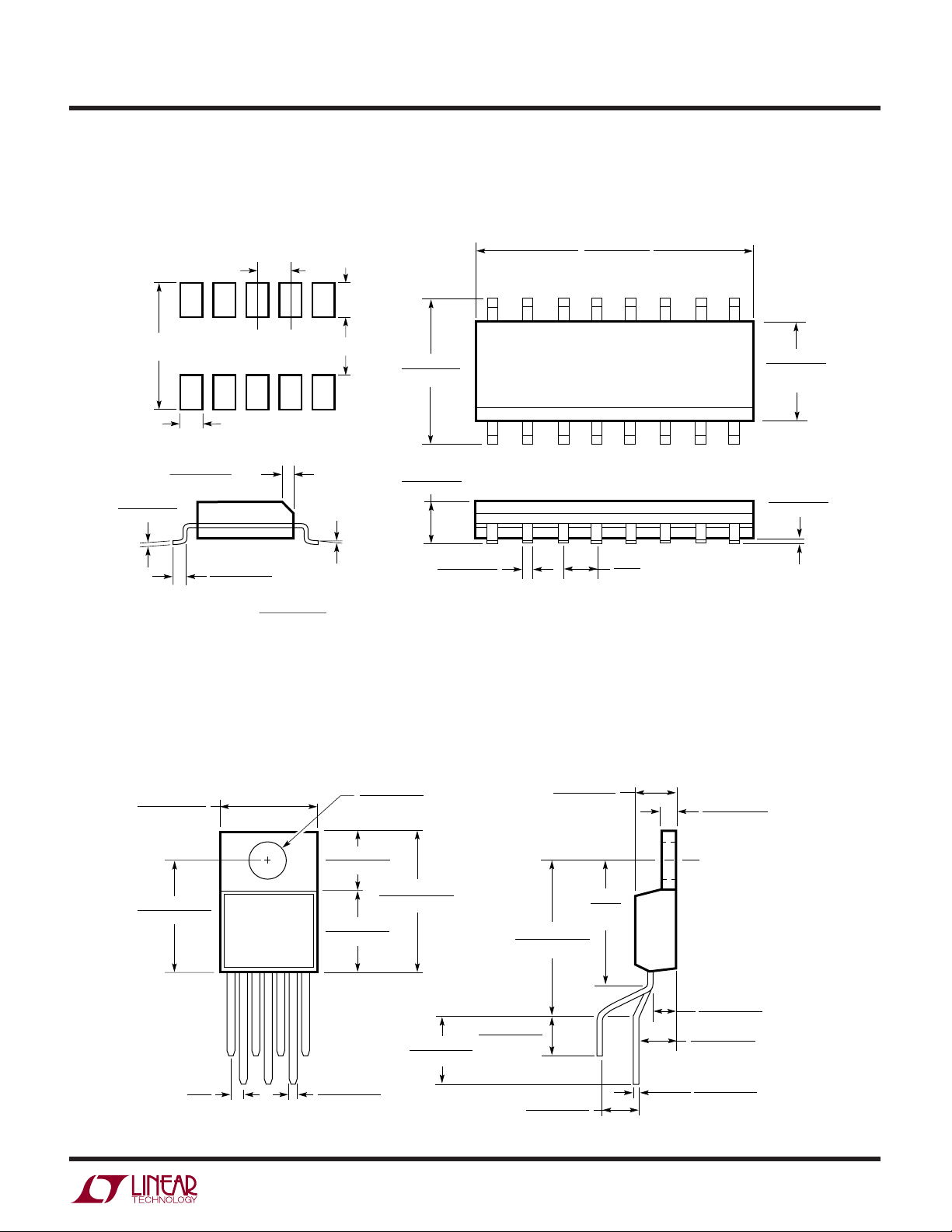
PACKAGE DESCRIPTION
16-Lead Plastic Small Outline (Narrow .150 Inch)
.050 BSC
N
.045 ±.005
U
S Package
(Reference LTC DWG # 05-08-1610)
16
LT1210
.386 – .394
(9.804 – 10.008)
NOTE 3
13
14
15
12
11
10
9
.245
MIN
.030 ±.005
TYP
(0.254 – 0.508)
.008 – .010
(0.203 – 0.254)
.160 ±.005
123 N/2
RECOMMENDED SOLDER PAD LAYOUT
.010 – .020
NOTE:
1. DIMENSIONS IN
2. DRAWING NOT TO SCALE
3. THESE DIMENSIONS DO NOT INCLUDE MOLD FLASH OR PROTRUSIONS.
MOLD FLASH OR PROTRUSIONS SHALL NOT EXCEED .006" (0.15mm)
×
°
45
.016 – .050
(0.406 – 1.270)
(MILLIMETERS)
0° – 8° TYP
INCHES
.228 – .244
(5.791 – 6.197)
.053 – .069
(1.346 – 1.752)
.014 – .019
(0.355 – 0.483)
N
1
TYP
T7 Package
7-Lead Plastic TO-220 (Standard)
(Reference LTC DWG # 05-08-1422)
.150 – .157
(3.810 – 3.988)
NOTE 3
N/2
4
5
.050
(1.270)
BSC
3
2
7
6
8
.004 – .010
(0.101 – 0.254)
S16 0502
.390 – .415
(9.906 – 10.541)
.460 – .500
(11.684 – 12.700)
.050
BSC
(1.27)
.147 – .155
(3.734 – 3.937)
DIA
.230 – .270
(5.842 – 6.858)
.570 – .620
(14.478 – 15.748)
.330 – .370
(8.382 – 9.398)
SEATING PLANE
.152 – .202
.260 – .320
(6.604 – 8.128)
.026 – .036
(0.660 – 0.914)
Information furnished by Linear Technology Corporation is believed to be accurate and reliable.
However, no responsibility is assumed for its use. Linear Technology Corporation makes no representation that the interconnection of its circuits as described herein will not infringe on existing patent rights.
(3.860 – 5.130)
.165 – .180
(4.191 – 4.572)
.700 – .728
(17.780 – 18.491)
.135 – .165
(3.429 – 4.191)
.620
(15.75)
TYP
(3.937 – 4.953)
*MEASURED AT THE SEATING PLANE
.045 – .055
(1.143 – 1.397)
.095 – .115
(2.413 – 2.921)
.155 – .195*
.013 – .023
(0.330 – 0.584)
T7 (TO-220) 0801
1210fa
15
Page 16

LT1210
TYPICAL APPLICATION
Wideband 9W Bridge Amplifier
U
15V
INPUT
5V
P-P
+
LT1210
–
–15V
SD
15V
10nF
–
LT1210
+
–15V
SD
10nF
RELATED PARTS
T1*
1
680Ω
100nF
220Ω
1
910Ω
* COILTRONICS Versa-Pac
OR EQUIVALENT
P
O
9W
1
1
1
1
TM
CTX-01-13033-X2
R
50Ω
9W
Frequency Response
L
1210 TA07
26
23
20
17
14
11
GAIN (dB)
8
5
2
–1
–4
10k 1M 10M 100M
100k
FREQUENCY (Hz)
1210 TA08
PART NUMBER DESCRIPTION COMMENTS
LT1010 Fast ±150mA Power Buffer 20MHz Bandwidth, 75V/µs Slew Rate
LT1166 Power Output Stage Automatic Bias System Sets Class AB Bias Currents for High Voltage/High Power
Output Stages
LT1206 Single 250mA, 60MHz Current Feedback Amplifier Shutdown Function, Stable with CL = 10,000pF, 900V/µs
Slew Rate
LT1207 Dual 250mA, 60MHz Current Feedback Amplifier Dual Version of LT1206
LT1227 Single 140MHz Current Feedback Amplifier Shutdown Function, 1100V/µs Slew Rate
LT1360 Single 50MHz, 800V/µs Op Amp Voltage Feedback, Stable with CL = 10,000pF
LT1363 Single 70MHz, 1000V/µs Op Amp Voltage Feedback, Stable with CL = 10,000pF
LT 0406 REV A • PRINTED IN USA
16
Linear Technology Corporation
1630 McCarthy Blvd., Milpitas, CA 95035-7417
(408) 432-1900 ● FAX: (408) 434-0507
●
www.linear.com
© LINEAR TECHNOLOGY CORPORATION 1996
1210fa
 Loading...