

Page 1
Engineer To Engineer Note EE-34
T
Notes on using Analog Devices’ DSP, audio, & video components from the Computer Products Division
Phone: (800) ANALOG-D or (781) 461-3881, FAX: (781) 461-3010, EMAIL: dsp.support@analog.com
Understanding 21xx/218x
EZ-ICE Theory of Operation To
Aid In Designing An EZ-ICE
Compatible Target
Last Modified: 4/14/98
Overview
This EE Note will give some insight into how an ADSP21xx or ADSP-218x Emulator DSP is powered up when
connected to an ADDS-21xx/ADDS-218x EZ-ICE. This
document can be used as a debugging tool and may
provide some clues into what is physically occurring in
your system if you are experiencing EZ-ICE power up
problems.
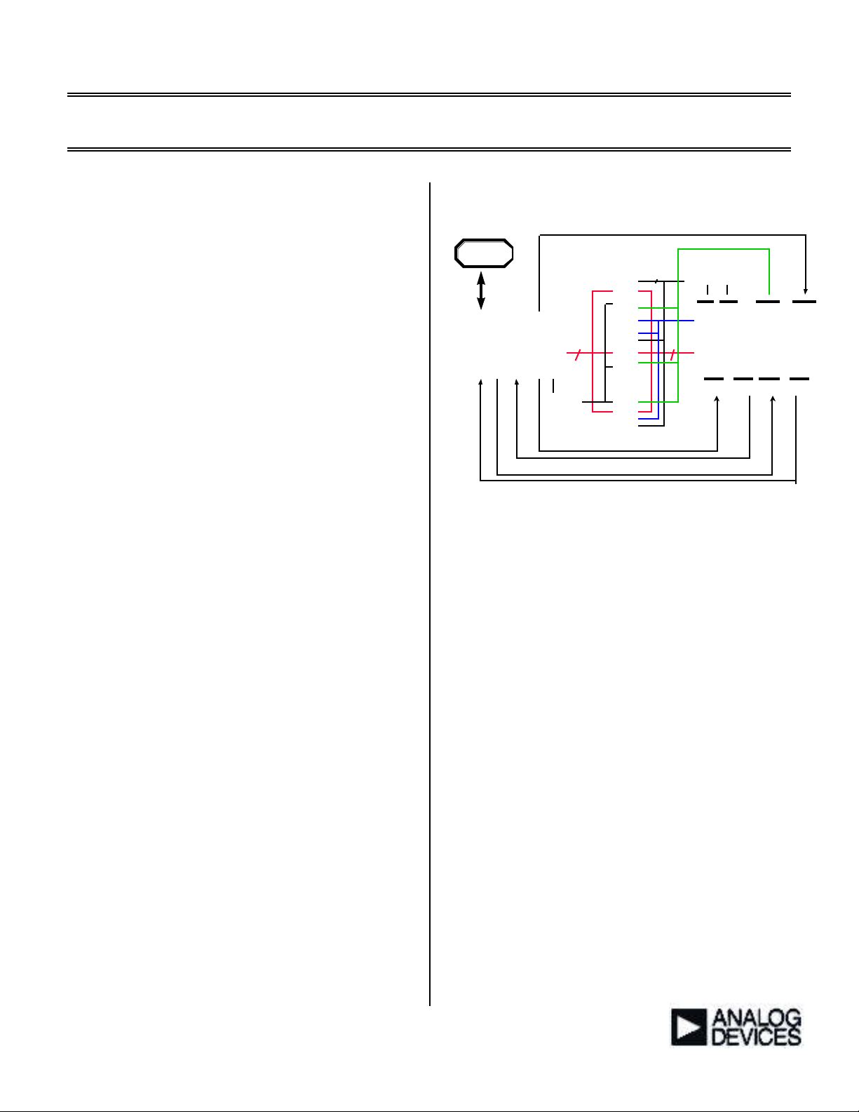
RS-232
Microcontroller
Block Diagram of a 21xx EZ-ICE
Port
Intel
80c31
3 bytewide bi-directional
trancievers 74F652s
x-
ceiver
8
Control
Logic
x-
ceiver
x-
ceiver
2
D0-D23
Read/Write
Logic
EMS
WR
A0
ADSP-21xx
Emulator DSP
EBRRDEBG BR BG
EIN
General EZ-ICE Theory of Operation
All ADSP-2100 Family emulators contains an Intel
80C31 ( or compatible 8051/8051 micro) host
microcontroller that performs the RS232 communication
to the PC as well as interpret the emulator commands
from the host computer at the other end of the RS232
line. The handshake mechanism for the 80C31 and the
ADSP-2100 Family DSP is done through the use of the
emulator interrupt (/EINT), emulator memory select
(/EMS), and the /BR and /BR pins.
The Bus Request (/BR) and Bus Grant (/BG) pins are
used to provide a handshake between the 80C31 and the
DSP. The ADSP-2100 Family instructions and data are
fed by the host PC to the 80C31. This two way
communication allows information to be passed from the
host PC to the DSP and from the DSP to PC. The /BR
and /BG handshake is used by the 80C31 allows for
effectively single stepping the ADSP-21xx through
emulator space code.
To achieve the actual data transfer, three byte-wide bidirectional latches are used as the communications port
between the 80C31 host and the ADSP-21xx Emulator
DSP. These latches are memory mapped into the data
memory space of the 8031 and the EZ-ICE memory space
of the DSP. The host can load or read each latch, one at
a time to construct or read a 24 bit instruction or 16 bit
data word. The DSP can read or write all 24 bits of the
three latches at once.
Whenever the 8031 host needs to intervene and
communicate with the DSP, it asserts the emulator
interrupt (/EINT) of the ADSP-21xx DSP. Halting on
breakpoints, single stepping, or halting the DSP from the
PC’s keyboard will result in the emulator interrupt pin for
the ADSP-21xx DSP to be asserted. When the DSP
reacts to the interrupt it will then vector to location 0 of
the emulator memory space while at the same time, the
emulator memory select line (/EMS) is asserted. The 24
bit instruction or data is then fetched from the 3 byte wide
latches. At the same time, interface logic between the
host and the PC will detect the /EMS line’s assertion and
immediately respond by asserting Bus Request. Once the
transfer has completed, the DSP returns from emulator
space. For software breakpoints, a TRAP instruction is
placed at the PM location where the breakpoint had been
set in the emulator software. The execution of a TRAP
instruction also forces an emulator interrupt.
To summarize, the Intel 80C31 microcontroller on the
EZ-ICE board provides RS232 communications between
the host PC and the DSP. When sending instructions to
the DSP, the microcontroller uses the /BR and /BG lines
in conjunction with the emulator interrupt features of the
DSP to effectively single step through code residing in the
DSP’s Program Memory.
Page 2

The Booting Sequence of the Emulator
DSP in an EZ-ICE Compatible Target
What exactly occurs when the EZ-ICE tries to establish
communications with a target system? This is important
in understanding why some emulated target systems fail
when an EZ-ICE is attached. The following steps describe
what occurs whenever the EZ-ICE is powered up or reset:
1) At EZ-ICE power-up or reset (red/black button pushed),
the Intel 80c31 microcontroller boots it’s monitor code
from its EPROM/EEPROM to on board SRAM.
2) During booting and initialization of the monitor
program, the DSP is still held in reset by the micro with
the /RESET signal held low. The DSP is held low until
the required 2000 CLKIN cycles and then released.
3) The DSP detects the EE ( Emulator Enable ) signal at a
logic high level, and comes out of reset with it’s
emulation circuitry enabled. The Emulator DSP
immediately looks at the state of the MMAP and BMODE
pins to determine how it will boot. For the ADSP-218x
variants, the DSP will look at the MODEx pins.
Memory Space can be thought of as a 3rd memory space
for the DSP, where the data is read/written to 2 memory
locations which are physically bi-directional latches. The
assertion of /EMS by the DSP indicates that the fetching
of the 1st instruction for the emulator interrupt service
routine is occuring.
7) The /EMS signal is also used to initial a bus request.
The Microcontroller recognizes /EMS line going active
and immediately asserts /EBR.
8) /EBG is given by the DSP when it recognizes /EBR.
9) The microcontroller downloads 24 bytes of test
information in the 3 bytewide bi-directional transceivers (
the 74F652s). This is actually a 24-bit instruction that is
loaded. A test NOP instruction is executed by the DSP as
it is fetched from the 3 byte wide latches.
- If the EZ-ICE initialization is successful to this point,
then this means the DSP has a clean CLKIN signal and
/RESET circuitry, the DSP is active and responding to
interrupts, and the /BR signal is functional.
4) The DSP will initiate its boot from an EPROM in
boot ( or byte ) memory space, from the IDMA port (
ADSP-218x), or from the HIP ( ADSP-2111 and ADSP-
2171). The Intel 80c31 host microcontroller during this
time holds /EINT low to assert an emulator interrupt so
that it’s next test will be performed. The microcontroller
will test the EZ-ICE handshake circuitry and verify the
DSP communications are working correctly. The
handshake process is done through the use of the emulator
interrupt( /EINT), emulator memory select (/EMS) and the
bus request (/BR) and bus grant (/BG) pins.
5) The DSP finishes booting and immediately services the
/EINT signal from the Intel Microcontroller. The /EINT
signal has the highest priority in emulation mode. The
handshake test by the microcontroller begins. The /EINT
signal is normally used for halting the DSP on
breakpoints, single stepping, or haltin on user
intervention.
6) The emulator DSP will recognize and respond to the
interrupt by vectoring to Emulator Memory Space which
causes the DSP asserts it’s /EMS signal. Emulator
10) The Emulator released /EBR.
11) The DSP Decodes and Executes the NOP instruction
and fetches the nest instruction from the interface circuitry
in Emulator Memory Space and it will halt.
12) The DSP writes a test value to the bi-directional
transceivers.
13) The Microcontroller reads the value returned back and
compares it to what it expects to see. The micro should
see the expected value, it if does then everything is
operational.
Thus, The DSP in Emulator Memory Space will:
- Fetch an instruction from latches
- Decode the instruction
- and write back to EM Space
EE-34 Page 2
Notes on using Analog Devices’ DSP, audio, & video components from the Computer Products Division
Phone: (800) ANALOG-D or (781) 461-3881, FAX: (781) 461-3010, EMAIL: dsp.support@analog.com
Page 3

An RTI instruction (return from emulator interrupt) can be
P
RS-232
Port
sent to the latch after all instructions have been loaded
which will cause the DSP to return from Emulator
Memory Space to User Space ( normal mode of
operation).
only active during data transmission. The data sent
between the DSP and Micro are sent via the ELOUT
and ELIN signals.
14) The micro plays with /EMS signal to make it
periodically blink. At this moment it is safe to assume
the EZ-ICE hardware is fully operational, and the target
system is ready for emulation from the PC.
15) The micro is ready for RS232 data from the host PC,
put into standby/ready state.
16) User invokes the EZ-ICE software from the DSP.
After the PC and host microcontroller downloads all DSP
registers and code, the /EINT signal does an RTI when the
host PC says to run, thus causing the DSP to return from
Emulator Interrupt. At the point the DSP is running as if
the EZ-ICE is not attached to the target system.
• The /BR and /BG pins are used to hand feed
instructions from the PC and host microcontroller.
Information is passed either from the DSP to the
micro, or from the micro to the DSP.
• The target /RESET signal is gated by the emulator to
prevent the assertion of /RESET during emulation
mode. The gating logic introduces a propagation
delay of approximately 12ns worst case. During full
speed operation in emulation ‘run’ mode, the target
/RESET will connect through the gating logic to the
target DSP. At all other times, the emulator locks
out the target /RESET from the DSP. The target
/RESET will product an interrupt request for the
80c31 which will be latched and serviced when
possible.
Block Diagram of a 218x EZ-ICE
3 bytewide bi-directional
trancievers 74F652s
x-
ceiver
Intel
8
80c31
Microcontroller
Control
Logic
ceiver
ceiver
x-
x-
Here are better descriptions of the pins on the ADSP-218x
DSP 14-pin emulator header:
Pin Name Description Destination
1 GND Common Ground. ALL
2 /BG Bus Grant to target Target
3 /EBG Emulator controlled Bus Grant 218x
4 /BR Bus request Emulator
5 /EBR Emulator controlled Bus Request 218x
6 /EINT Emulator Interrupt pin 218x
7 KEY Key pin None
8 ELIN Emulator data in 218x
9 ELOUT Emulator data out Emulator
10 ECLK 16.67 Mhz gated clock 218x
11 EE Emulator Enable 218x
12 /EMS Emulator Memory Select Emulator
13 /RESET DSP Reset Emulator
14 /ERESET Emulator controlled Reset 218x
Additional 218x Information
The 218x DSP puts the BG pin in a high impedance state
when the emulator is plugged in. The emulator gates the
2181's Emulator Bus Request (/EBG) and drives the /BG
signal when the emulator is running user code.
Read/Write
D0D23
Logic
A0
FPGA
WR
ECLK
ELIN
ELOUT
EMS
ADSP-21xx
Emulator DS
EBRRDEBG BR BG
2
EINT
The 218x DSP also ignores the /RESET pin when the
emulator is plugged in. The emulator gates the target's
Emulating ADSP-218x Targets:
/RESET pin and drives the Emulator Reset (/ERESET)
pin on the 218x (which actually causes the 218x to reset).
• For the ADSP-218x DSPs, the 3 bytewide
directional transceivers are interfaced to an
You should not need any jumpers to isolate signals.
FPGA which converts the parallel 24 bit
information to serial data using a Parallel
to Serial Shift Register. Data is sent to the
DSP as 40 bit information with header/packet
information. The ECLK signal is a gated clock and
EE-34 Page 3
What Can Prevent The MicroController
From Gaining Control of the DSP via the
Emulator Interrupt?
Notes on using Analog Devices’ DSP, audio, & video components from the Computer Products Division
Phone: (800) ANALOG-D or (781) 461-3881, FAX: (781) 461-3010, EMAIL: dsp.support@analog.com
Page 4

ANS: Higher Priority 218x Instruction Cycle Boundary
Cycle Steal Requests. The ADSP-218x Priority Chain
for concurrent requests occurring at instruction cycle
boundaries is as follows:
ADSP-218x PRIORITY CHAIN
1. COMPLETION OF AN EXTERNAL MEMORY ACCESS
2. IDMA INTERNAL MEMORY TRANSFERS
3. BDMA INTERNAL MEMORY TRANSFERS
4. SPORT AUTOBUFFER OPERATIONS
5. EMULATOR INTERRUPT
6. EMULATOR INSTRUCTION
7. POWERDOWN INTERRUPT
8. UNMASKED INTERRUPT
9. NORMAL INSTRUCTION EXECUTION
10. BYTE MEMORY ACCESSES
Thus, other cycle steal requests at instruction cycle
boundaries can cause the emulator software to crash when
attempting to halt the EZ-ICE ( Error 166: DSP Not
Responding To Emulator Interrupt ). This can
happen when there are multiple external wait-stated
accesses, IDMA or BDMA transfers, because in any given
cycle, these cycle steals have higher priority to be serviced
than the emulator interrupt.
Target Hardware Recommendations
There are certain hardware requirements that we suggest
you follow in order to allow minimal troubleshooting
time for a failing EZ-ICE system. The following
recommendations are followed by a description of why it
is needed. Most of these suggestions are the result of
previous user’s questions and problems, and will thus
provide the EZ-ICE user with valuable tips.
1) Bus Request (/BR) should be pulled high
with a 10 Kohm resistor.
Failure to pull /BR high may result in the inability of the
EZ-ICE to fully initialize when connected to a target. It
is critical for /BR not to be left floating, even if you are
not using it in your target, because of the Intel 80c31
using /BR to communicate with the DSP.
Remember, the EZ-ICE includes 3 byte-wide transceivers
to exchange data with the Intel 80C31 using the data bus
lines D0-D23 and /BR.
Typical symptoms of this problem would be indicated by
the host emulator software. For example, the user may
see “ Fatal Firmware Error #174” , indicating that the
Intel 80c31 was unable to successfully communicate with
the DSP, since it could not acquire the bus with the/BR
pin.
2) Pull-up all memory select signals high for
EZ-ICE emulator compatibility.
You must connect a pull-up resister ( 10 Kohm) on the
memory select signals (/RD, /WR, /PMS, /DMS, /BMS,
/CMS, and /IOMS) if they are used in your target ( for
example, using external memory or memory-mapped
peripheral devices). The pull-up resisters are needed since
there are no internal pull-ups to guarantee their state
during prolonged tri-stated conditions resulting from
typical EZ-ICE debugging sessions. The EZ-ICE uses
the DSP’s bus to communicate with PM, DM, BM and
Emulator Memory Space. The Emulator DSP used the
/WR and /RD line to send or capture data from the 3 byte
wide bi-directional transceivers. These resistors may be
removed when the EZ-ICE is not being used.
WARNING: Bus contention can result from a failure to
use both memory select signals (/PMS, DMS and /BMS)
in your design. Target memory ( or memory-mapped
peripheral devices) would contend with emulator memory,
while the EZ-ICE is attempting to execute its monitor
code. This bus contention will result in faulty operation
and may even damage your EZ-ICE, your target, or both.
A typical symptom of EZ-ICE bus contention with
devices on your target would be the failure of the green
LED on the EZ-ICE to blink while connected to the
target. One way to diagnose which pins are causing the
contention would be to disconnect the PGA to PGA
adapter on the EZ-ICE and remove the data bus pins one
by one on the connector. Keep bringing up the EZ-ICE
until you are able to see the green LED flashing. This
will help you isolate which pin or pins are suspect. We
have seen this problem occur with users who have
memory mapped peripherals or FPGAs that strobe the
/RD or /WR lines (These memory strobes are used by the
INTEL 80C31 on power-up to send and retrieve
diagnostics information executed from its monitor code).
NOTE: This isolation technique is not applicable to the
ADSP-2181 target, since it only uses the 14 pin EZ-ICE
port for DSP emulation. The same also applies to
ADSP-2171 targets since its design does not use a PGA
to PGA connector.
3) Interfacing to External Memory
Design your Program Memory ( PM), Data Memory
(DM), and Boot Memory ( BM) external interfaces to
comply with worst case device timing requirements and
EE-34 Page 4
Notes on using Analog Devices’ DSP, audio, & video components from the Computer Products Division
Phone: (800) ANALOG-D or (781) 461-3881, FAX: (781) 461-3010, EMAIL: dsp.support@analog.com
Page 5

switching characteristics as specified in the DSP’s data
sheet. The performance of the EZ-ICE may approach
published worst case specification for some memory
access timing requirements and switching characteristics.
This is due to increased loading of the DSP’s busses by
emulator circuitry. For complete information on interface
timing, see the data sheet corresponding to the DSP used
in your design.
NOTE: If your target does not meet the worst case chip
specification for memory access parameters, you may not
be able to emulate your circuitry at the desired CLKIN
frequency. Depending on the severity of the specification
violation, you may have trouble manufacturing your
system as DSP components statistically vary in switching
characteristic and timing requirements within published
limits.
6) Use a Schmitt Trigger on the Reset Line
connected between the RC circuit and /RESET
The use of an RC circuit to delay the deassertion of the
reset line at power-up is not recommended for higher speed
systems such as the ADSP-2100 family. /RESET needs
to be held low on power-up of the DSP for a minimum
2000 DSP CLKIN cycles to ensure that CLKOUT phaselocks with CLKIN. The ADSP-2100 Family DSP will
switch too fast on deassertion, and the target DSP will
lock up since the /RESET line will bounce up and down
before settling. This will cause the DSP to lock up since
/RESET will go below and cause a faulty reset that does
not meet the 2000 DSP cycle specification. A Schmitt
Trigger will minimize the ringing on the reset line and
thus guarantee proper DSP power-up and initialization.
4) Overlay Memory (Does not apply for the
2181 and 218x EZ-ICEs)
If you plan to use EZ-ICE board overlay memory you
must remove your target board’s memory and memory
mapped peripherals located on the overlay memory space (
DM or PM). Removing the target memory and memory
mapped peripherals avoids bus contention between them
and the EZ-ICE board overlay memory.
The overlay memory jumper setting (JP1) on the 2181
EZ-ICE is no longer applicable and therefore is note used.
EZ-ICE overlay memory is not the same as the ADSP2181’s Overlay Memory Space.
5) Place 0.1 uF decoupling capacitors on all
VDD pins connected to the same digital ground
as close to the DSP as possible.
Decoupling capacitors provide a localized source DC
voltage and current for optimal operation of the DSP
during clock and data transitions when all signal pins
switch simultaneously. Decoupling also ensures that
there is a low-impedance power source present in power
planes and circuit traces. High-frequencies are effectively
removed from the signal trace while lower frequencies
remain unaffected.
Also make sure that all other digital IC chips in your
system are properly decoupled to manufacturers
recommendations.
Also, a 100 uF bypass capacitor can be placed at the rails
of the power supply coming into the target board to filter
unwanted RF noise from the power supply cable.
7) Clock Source Selection
(Not applicable for the 218x EZ-ICE
Emulator)
You can configure the EZ-ICE board to use either the EZICE board’s on-board oscillator or your target’s oscillator
as the CLKIN source for the EZ-ICE board’s DSP. There
are performance tradeoffs on each case.
Selecting the EZ-ICE board’s oscillator as the CLKIN
source for the DSP generally results in more reliable
execution of the DSP. This reliability stems from the
short distance traveled by the clock signal and having both
the DSP and oscillator use the same power and ground
planes.
Selecting the target’s oscillator as the CLKIN source for
the DSP sometimes results in faulty operation of the
system. These faults stem from the much greater distance
over which the target-based oscillator must drive the clock
signal ( through several terminations). Depending on the
target system layout and oscillator driving capabilities, the
resulting clock signal may be fairly distorted by the time
it reaches the EZ-ICE board’s DSP. If your system works
with the target’s oscillator providing the EZ-ICE board
clock source, then it will almost certainly work when the
DSP replaces the EZ-ICE board. This is not nearly as
certain if using the EZ-ICE board’s oscillator as the clock
source.
Whether the clock source is on the EZ-ICE board or
target, CLKIN may never exceed the tested frequency limit
of the EZ-ICE board’s DSP device. The speed grade
branded on the top of the DSP corresponds to four-times
the maximum CLKIN frequency of the processor.
EE-34 Page 5
Notes on using Analog Devices’ DSP, audio, & video components from the Computer Products Division
Phone: (800) ANALOG-D or (781) 461-3881, FAX: (781) 461-3010, EMAIL: dsp.support@analog.com
Page 6

We also recommend using an oscillator for your target vs.
using a crystal. On oscillator will result in more reliable
operation of the DSP.
8) Board Recommendations
Whenever possible, target systems should consist of a
multilayered PCB board with a separate power and ground
plane stacked in the middle layers of the board.
Wirewrapped boards are not generally recommended as
they are more susceptible to external noise and parasitic
capacitance.
Warning: The DSP on your EZ-ICE board is sensitive
to CMOS latchup. Latchup occurs when power is applied
to an EZ-ICE board which is plugged into a target that has
already been powered. If you power your EZ-ICE board
under these conditions, it is likely that the EZ-ICE board’s
DSP will be damaged and will subsequently malfunction.
Take great care to always observe the correct power up
procedure.
Other Target Design Considerations:
- EZ-ICE emulation introduces an 8 ns propagation delay
between the target circuitry and the DSP on the /RESET
signal.
9) Use a power supply that supplies 1000 mA
current
The EZ-ICE needs approximately 800 mA from a 5 Volt
supply in order to operate correctly. If a lower current is
supplied, the EZ-ICE may fail to power up correctly.
10) Recommended EZ-ICE Power-up Procedure
( for the 2101, 2111 and 2171 EZ-ICEs)
The EZ-ICE board communicates with a host PC over an
RS232 serial cable. You must use the COM1 or COM2
serial port on your PC. Connect the EZ-ICE board to the
selected COM port using the RS232 cable shipped with
your EZ-ICE package.
Ideally you should use the same +5 Volt source for the
EZ-ICE board as you use for your target. This reduces the
steps for applying power to the emulation system and lets
you apply and remove power to both simultaneously.
However, you do use separate power supplies, the
following must be done:
1. With the power off, insert the EZ-ICE board in your
target system.
- EZ-ICE emulation introduces an 8 ns propagation delay
between your target circuitry and the DSP on the /BR
signal.
- EZ-ICE emulation ignores /RESET and /BR when
single-stepping.
- EZ-ICE emulation ignores /RESET and /BR when in
Emulator Space (DSP Halted).
- EZ-ICE emulation ignores the state of target /BR in
certain modes. As a result, the target system may only
take control of the DSP’s external memory bus only if
bus grant (/BG) is asserted by the EZ-ICE board’s DSP.
- EZ-ICE emulation introduces a 500 us latency between
transitions to User Space and some signal responses.
This occurs when you start ( or resume) running your
DSP program. The latency is the time between
resumption of code execution and the EZ-ICE board
allowing the DSP to respond to /RESET and /BR. For
more information on Emulator Space, User Space, and
other EZ-ICE mode topics, refer to the ADSP-2100
Family EZ-Tools Manual.
2. Apply power to the EZ-ICE board.
3. Apply power to the target.
4. Invoke the emulator software.
5. Reverse this process for removing power from the
system. Power down the target first, then the EZ-ICE.
** See ‘Emulating on an ADSP-2181 Target’ for proper
power-up sequence for the 2181 EZ-ICE.
EE-34 Page 6
Notes on using Analog Devices’ DSP, audio, & video components from the Computer Products Division
Phone: (800) ANALOG-D or (781) 461-3881, FAX: (781) 461-3010, EMAIL: dsp.support@analog.com
 Loading...