Page 1

Engineer-to-Engineer Note EE-244
a
Technical notes on using Analog Devices DSPs, processors and development tools
Contact our technical support at dsp.support@analog.com and at dsptools.support@analog.com
Or vi sit our o n-li ne r esou rces htt p:/ /www.analog.com/ee-notes and http://www.analog.com/processors
Interfacing Gated Clocks to ADSP-21065L SHARC® Processors
Contributed by Aseem Vasudev Prabhugaonkar and Jagadeesh Rayala Rev 1 – September 29, 2004
Introduction
The serial ports (SPORTs) on ADSP-21065L
SHARC® processors are designed for
continuous clock operation. This application note
discusses gating the SPORT clock as required in
SPI-compatible operation modes. In this EENote, SPI is considered a standard interface to
the ADSP-21065L processor's SPORT to explain
SPORT functionality when an external gated
clock is applied to the SPORT.
The SPI master interface to the ADSP-21065L
SPORT is a generic platform that benefits system
designs that interface devices such as analog-todigital converters that use a gated clock or
similar timing requirements.
audio codecs), and TDM (time division
multiplex) multi-channel mode.
The SPORTs can operate with little endian or big
endian transmission formats, and with selectable
word lengths of 3 to 32 bits. SPORT clocks and
frame syncs can be generated internally or
externally.
About ADSP-21065L Serial Ports
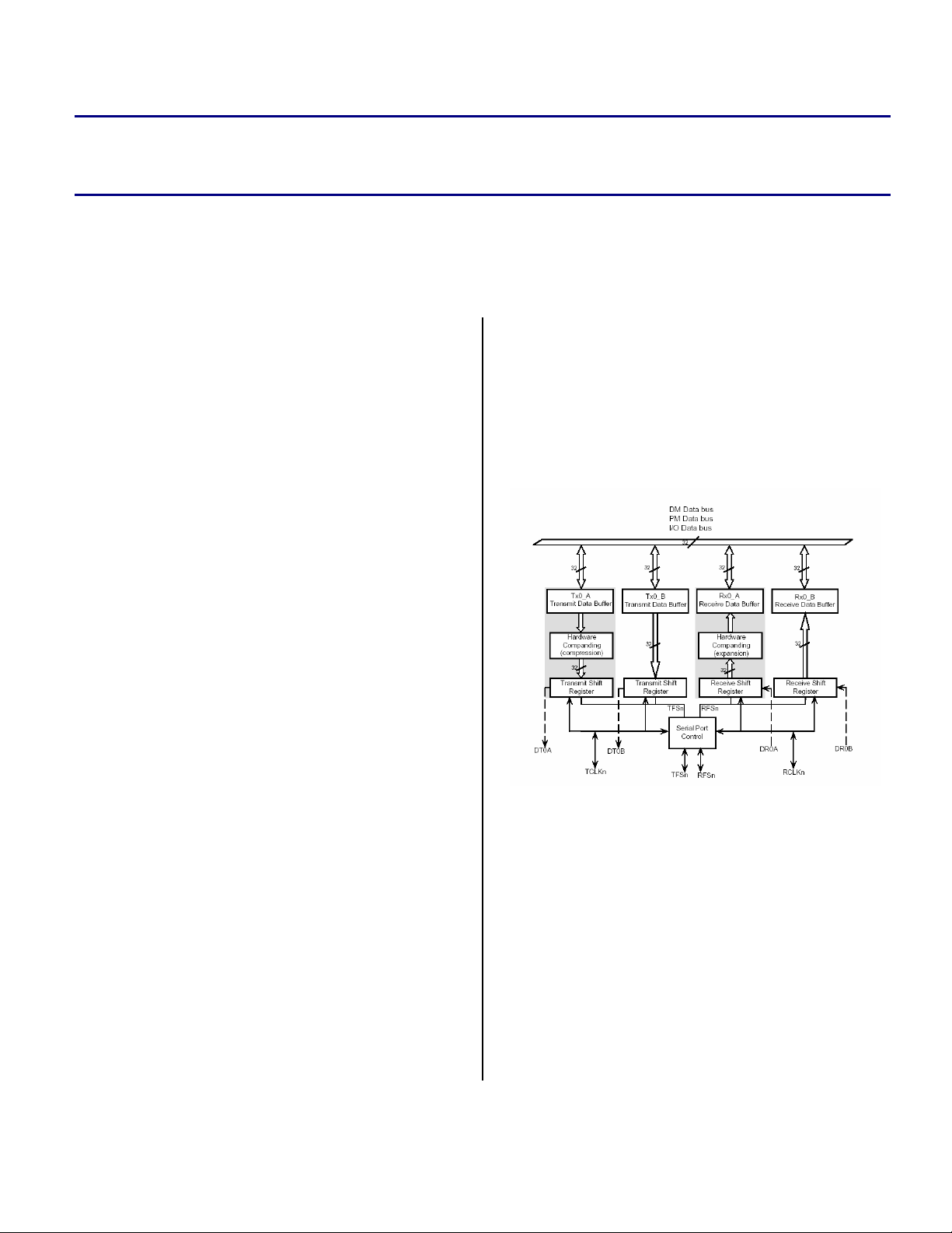
The ADSP-21065L SHARC processor includes
two synchronous SPORTs, which provide an
inexpensive interface to a wide variety of digital
and mixed-signal peripheral devices. The
SPORTs can operate at 1x CLKIN clock
frequency, providing a maximum data rate of
33 Mbit/s. Each serial port has a primary and a
secondary set of transmit and receive channels.
Independent transmit and receive functions
provide greater flexibility for serial
communications. Serial port data can be
transferred automatically to and from on-chip
memory via DMA. Each of the serial ports
supports three operation modes: DSP serial port
2
mode, I
Copyright 2004, Analog Devices, Inc. All rights reserved. Analog Devices assumes no responsibility for customer product design or the use or application of
customers’ products or for any infringements of patents or rights of others which may result from Analog Devices assistance. All trademarks and logos are property
of their respective holders. Information furnished by Analog Devices applications and development tools engineers is believed to be accurate and reliable, however
no responsibility is assumed by Analog Devices regarding technical accuracy and topicality of the content provided in Analog Devices’ Engineer-to-Engineer Notes.
S mode (an interface commonly used by
Figure 1. Serial Port Block Diagram
What is a Gated Clock
A gated clock is a discontinuous clock supplied
by external devices such as analog-to-digital
converters and SPI (Serial Peripheral Interface)
devices. When configured in master mode, these
devices generate a bit clock required for
transferring data. The clock is generated only
while the data is being transmitted out, hence the
term gated clock. Most analog-to-digital
converters gate the serial clock during signal
Page 2

a
conversion to achieve higher noise immunity.
Certain issues apply to the ADSP-21065L
processor's SPORTs when clocked externally.
Understanding these issues will help you design
interfaces to ADSP-21065L processor SPORTs.
Interfacing an ADSP-21065L
SPORT to an ADSP-21161N SPI
Master Device
In addition to four SPORT modules, the ADSP21161N SHARC processor features a second
SPORT designed for SPI operation. The
following setup uses the ADSP-21161N
processor as an example of other SPI master
devices such as analog-to-digital converters.
The analysis will help system designers
understand how SPORTs behave when clocked
externally.
ADSP-21065L
SPORT
RXD
RFS
MOSI
SPICLK SCLK
FLAGx
ADSP-21161
SPI MASTER
Modifying the SPORT word length inside the
first SPORT receive interrupt service routine
(ISR)
Modifying the SPORT word length inside the
external interrupt “IRQx” ISR.
Modifying the SPORT Word Length Inside the
First SPORT Receive ISR
This scenario (Figure 3) requires that:
The SPI drives data on the falling clock edge,
and the SPORT receives the data on the
rising clock edge. The 16-bit transmitted data
is 0xFF00.
The SPORT is initially configured for a 15-
bit word length and is then configured onthe-fly to a 16-bit word length inside the first
SPORT receive ISR.
Figure 2. Gated Clock Setup of the SPORT
As shown in
IRQx
Figure 2, the ADSP-21161 processor's SPI port
provides a serial clock and a data and frame sync
to the ADSP-21065L processor's SPORT. For
easy analysis, the master SPI sends a 16-bit data
word (
0xFF00) to the ADSP-21065L processor.
When configured for external clock
L
generation, the ADSP-21065L
processor's SPORTs require two serial
clock edges for synchronization.
This requirement demands special software
handling. While the master continues to transmit
16-bit words, the slave must alter the word
length at runtime to overcome this issue. There
are two approaches:
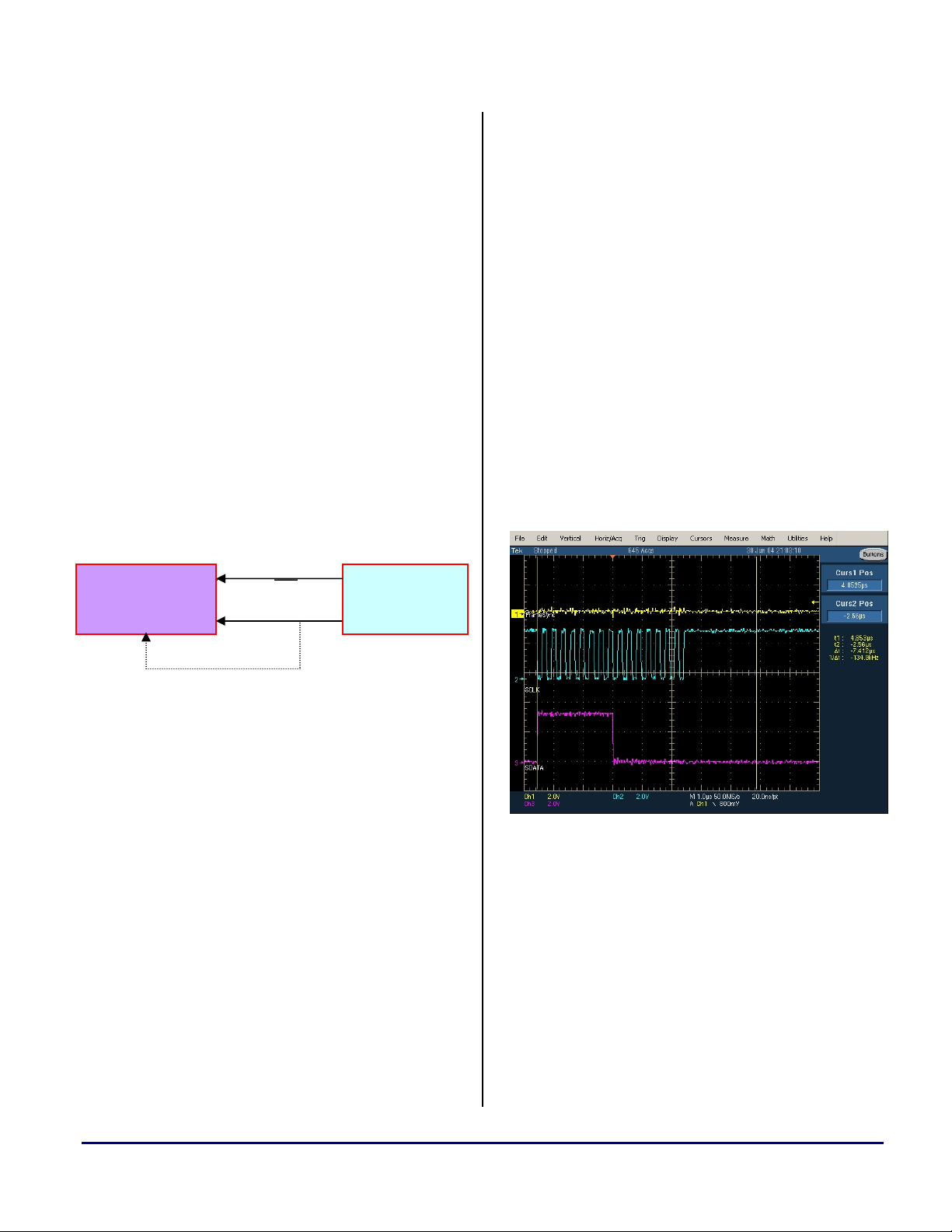
Figure 3. Modifying SPORT Word Length Within the
First SPORT Receive ISR
The data is driven on the falling serial clock
edges. The first two rising clock edges are
required for ADSP-21065L SPORT
synchronization. In this case, the SPORT is
programmed to latch data on the rising clock
edge. This means that the first two rising edges
are lost and no data is latched; hence, a complete
15-bit word is received at the end of the first
serial clock rising edge of the second transmitted
word. Thus, the MSB of second transmitted word
becomes the LSB of the first received word.
Interfacing Gated Clocks to ADSP-21065L SHARC® Processors (EE-244) Page 2 of 4
Page 3

a
Hence, the data received the first time the data
word length is 15 bits would be 0x7E01.
The word length changed inside the first serial
port ISR does not take effect for the second
word; hence, the second word length remains
configured as 15 bits. This means that the second
(15-bit) word reception ends at the end of second
(16-bit TX) transmitted word. The word length
change takes effect from the third word on,
implying that the reception of words three and
higher will be correct (0xFF00).
Modifying the SPORT Word Length Inside the
External Interrupt "IRQx" ISR
This scenario (Figure 4) requires that:
The SPI drives data on the falling clock edge,
and the SPORT receives data on the rising
clock edge. The transmitted 16-bit data is
0xFF00.
reception of first word is completed at the end of
first transmitted word. The SPORT starts to
receive 16-bit words correctly after the second
word.
Figure 4. Modifying SPORT Word Length Within the
External Interrupt "IRQx" ISR
The SPORT is initially configured for a 14-
bit word length and is then configured onthe-fly to a 16-bit word length inside the
external interrupt ISR.
The very first frame sync is used to generate
the external interrupt (IRQx) to the ADSP21065L processor. The word length is
modified on-the-fly to 16 bits inside the
IRQx ISR, not inside the serial port receive
ISR.
The first two rising edges of the SPORT clock
are required for SPORT synchronization. The
first frame sync generates an external interrupt to
the processor. Inside the external interrupt ISR,
the SPORT word length is modified from the
initial 14 bits to 16 bits. Note that this word
length change must occur after the two rising
edges.
The change in word length goes into effect after
the second word has been received. Since the
SPORT is initially configured for 14 bits, the
Conclusion
Based on these scenarios, you must consider two
options while designing an ADSP-21065L
system with a gated external serial clock:
In the first scenario, two initial dummy reads
are necessary. The SPORT would read the
16-bit data correctly from the third word on.
In the second scenario, the single initial
dummy read is necessary. However, the
processor must use one of its external
interrupts.
This approach is not limited to the ADSP21065L processor's SPORT interface with SPI.
It can be used to interface a range of external
devices such as analog-to-digital converters that
supply a gated serial bit clock for noise
immunity.
Interfacing Gated Clocks to ADSP-21065L SHARC® Processors (EE-244) Page 3 of 4
Page 4

a
Appendix
Refer to the receive code for the ADSP-21065L SPORT and the transmit code for the ADSP-21161N SPI
(master mode) in the attached ZIP file.
References
[1] ADSP-21065L EZ-KIT Lite Evaluation System Manual. Rev 2.0, January 2003. Analog Devices, Inc.
[2] ADSP-21161N EZ-KIT Lite Evaluation System Manual. Release 2.0, January 2003. Analog Devices, Inc.
Document History
Revision Description
Rev 1 – September 29, 2004
by Aseem Vasudev Prabhugaonkar
Initial Release
Interfacing Gated Clocks to ADSP-21065L SHARC® Processors (EE-244) Page 4 of 4
 Loading...