

Page 1

Engineer-to-Engineer Note EE-234
a
Technical notes on using Analog Devices DSPs, processors and development tools
Contact our technical support at dsp.support@analog.com and at dsptools.support@analog.com
Or vi sit our o n-li ne r esou rces htt p:/ /www.analog.com/ee-notes and http://www.analog.com/processors
Interfacing T1/E1 Transceivers/Framers to Blackfin® Processors via the
Serial Port
Contributed by K. Unterkofler and T. Lukasiak Rev 1 – May 11, 2004
Introduction
This EE-Note describes how to interface
Blackfin® processors to standard T1 or E1
encoded signals. The proposed template assumes
that a Blackfin processor is functionally located
between two T1/E1 streams to perform the
required processing, such as line echo canceling.
However, the Blackfin processor can be adapted
easily to other functional architectures. As shown
in this EE-Note, most standard backplane PCM
data streams interface directly to the processor’s
serial port(s), without any external hardware.
This document provides schematics, layout
suggestions, and a software framework for
receiving, processing, and transmitting PCM
streams between two T1/E1 transceivers/
framers.
The chosen framing device is the PMC-Sierra
PM4351 COMET. The PCM streams are
connected to one of the processor’s synchronous
serial ports (SPORTs), which can handle two
input streams and two output streams. The
COMET is configured via the processor’s
asynchronous memory interface in the external
bus interface unit (EBIU).
The schematics are intended to be for a daughterboard that plugs into an EZ-KIT Lite™
evaluation system available from Analog
Devices, Inc.
The application was implemented on and is
described herein for the ADSP-BF533 processor
Copyright 2004, Analog Devices, Inc. All rights reserved. Analog Devices assumes no responsibility for customer product design or the use or application of
customers’ products or for any infringements of patents or rights of others which may result from Analog Devices assistance. All trademarks and logos are property
of their respective holders. Information furnished by Analog Devices applications and development tools engineers is believed to be accurate and reliable, however
no responsibility is assumed by Analog Devices regarding technical accuracy and topicality of the content provided in Analog Devices’ Engineer-to-Engineer Notes.
[1], [2]. Though it is possible to apply this same
board to the ADSP-BF561 EZ-KIT Lite
evaluation system with only minor changes,
considering that this device incorporates two
cores and two SPORTs, it makes more sense to
extend the board to four COMET devices and to
allow it to handle twice the number of processed
channels [3].
The board was also designed to interface
!
also to a ADSP-BF535 processor,
although it requires more substantial
hardware changes, such as using two
SPORTs instead of the one needed for the
ADSP-BF533. The schematics refer to the
the required changes. This entails
significant software which are beyond the
scope of this EE-Note.
The software framework is written in C entirely.
All references to execution times are taken from
this code example.
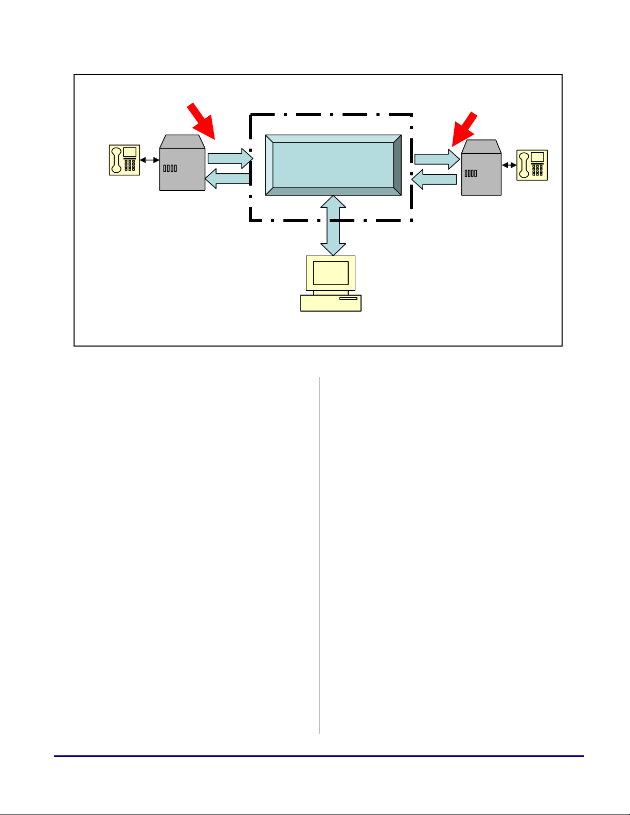
System Architecture
Figure 1 shows a block diagram of a typical
application. The board is designed to plug into an
existing T1/E1 connection via two RJ48C
connectors. This leads to two streams (stream 1
and stream 2), both carrying incoming and
outgoing data (R
most basic mode of operation (pass-through),
R
and SIN are copied unaltered to R
IN
S
respectively, such that the whole resembles
OUT,
the original single T1/E1 connection.
IN
, R
OUT
, S
and S
IN,
). In the
OUT
OUT
and
Page 2
a
T1/E1 Stream 1
T1/E1 Interface Board
Rin
Framing and
processing
Sout
Figure 1. System overview
The software also provides a parser-based UART
interface to a generic host processor for setting
operating modes and parameters and controlling
the Blackfin processor and the COMET framing
device.
Figure 2 provides a detailed view of the interface.
The signals from the two RJ48C connectors are
conditioned and isolated from the digital domain
by transformers. Also provided are over-voltage
protection diodes. The COMET framers
(PM4351) are configured to generate serial inputs
in a format compliant with the SPORT’s multichannel mode from the R
to generate the R
SPORT’s serial output data. The two COMET
framer chips are connected to the Blackfin
processor via the External Bus Interface Unit
(EBIU) and are configured via this interface.
OUT
and S
T1/E1 Data Formats
T1/E1 connections are a well-known and widely
adopted standard. For the purpose of this EENote, it is sufficient to say that T1 lines encode 24
and SIN streams, and
IN
streams from the
OUT
T1/E1 Stream 2
Rout
Sin
RS232 to Host
channels of 8-bit data plus one framing bit
(totaling 193 bits) into a 1.544 MHz carrier wave.
Similarly, E1 lines encode 32 channels of 8-bit
data (totaling 256 bits) into a 2.048 MHz carrier.
In both cases, this corresponds to a new sample of
each channel every 125 µs. The 8-bit data is
obtained from linear, 14- or 13-bit data samples
by compression according to a-law or µ-law,
respectively.
In addition to the data (sometimes referred to as
the payload), T1/E1 streams contain signaling bits
according to a variety of communication
standards. This EE-Note does not go into the
details of these standards, since the COMET
devices’ functionality is to extract the payload
from the incoming T1/E1 streams and to encode a
valid T1/E1 outgoing stream from the payload
from the DSP, according to the selected standard.
Thus, if the COMET devices are set up correctly,
the processor will “see” the payload only and
never have to handle the signaling bits. If errors
occur, the COMET can be set up to generate an
interrupt for the DSP as well. For more details,
refer to [4], [5] and [7].
Interfacing T1/E1 Transceivers/Framers to Blackfin® Processors via the Serial Port (EE-234) Page 2 of 13
Page 3
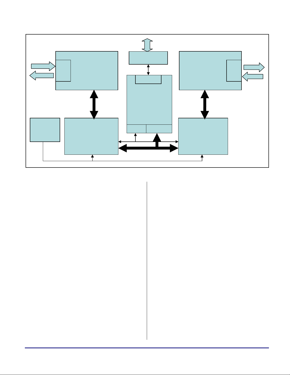
a
Rin
Line Interface
Protection
RJ48C
&
Isolation
RS232
Sout
EZ-KIT Lite
Expansion
Connectors
CLK
2.048MHz
COMET1
PM4351
Figure 2. T1/E1 Interface Card Block Diagram
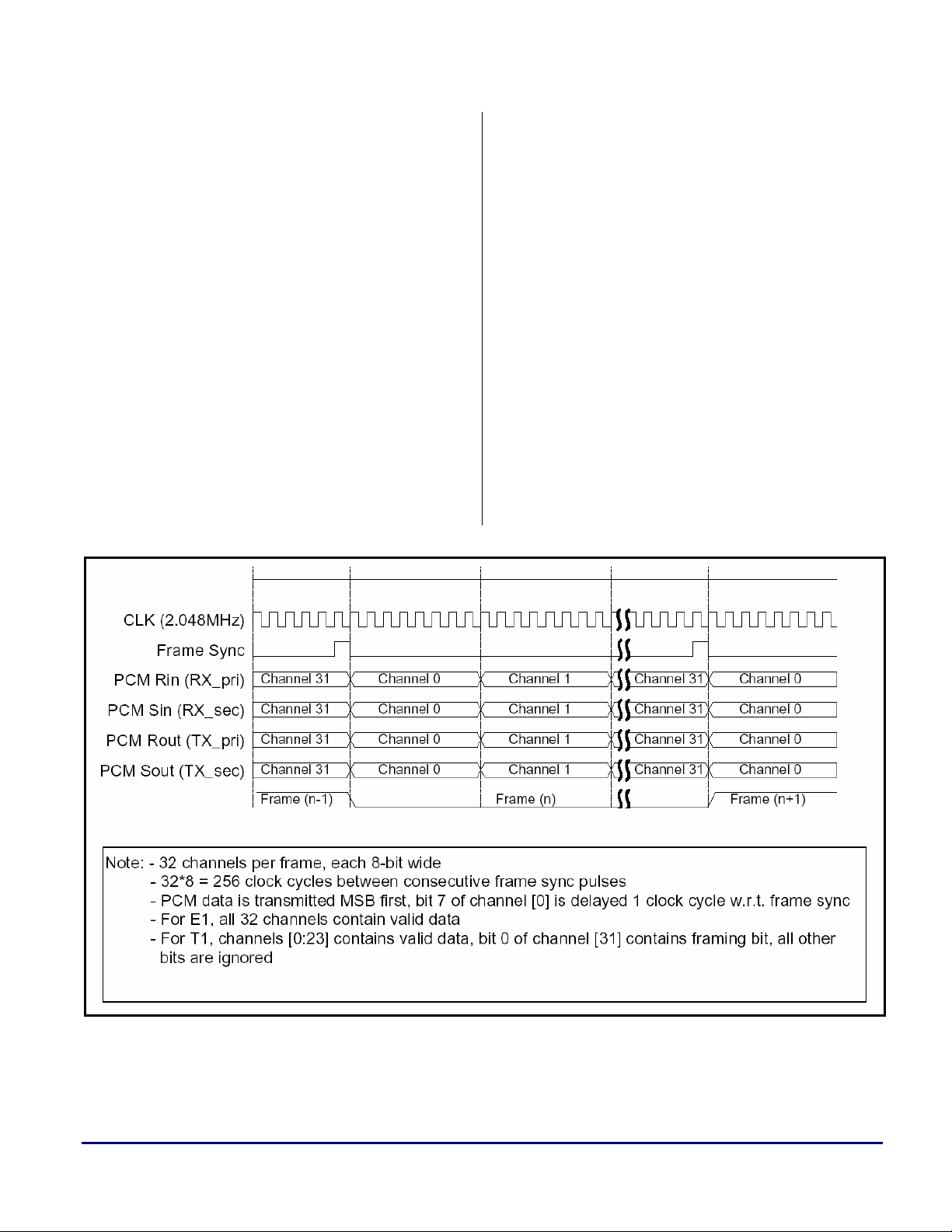
The incoming streams (RIN and SIN) are thus
converted (mapped) into a PCM data stream,
sometimes referred to as “backplane”. Again,
there are a variety of standards, but they consist of
a signal containing the data bits for each channel
and, for T1 lines, the framing bit, synchronous to a
1.544 (T1) or 2.048 MHz (E1) clock. This block
of data is called a frame. The beginning of a frame
is signaled by a separate signal called a “frame
sync”. For T1, the COMET also provides the
option of mapping the 24 channels into a
2.048 MHz backplane, such that channels 24-31
contain dummy data, which the processor can then
ignore. This offers the advantage that both T1 and
E1 settings use the same clock, thus switching
between the two formats requires only a simple
software change, rather than switching between
two clock sources.
For the outgoing streams (R
OUT
and S
OUT
considerations apply. The backplane signals
consist of 32 channels of 8-bit data for an E1 line.
Similarly, for a T1 line, the COMET simply
ignores channels 24-31.
EBIU SPORT
PCM data streams
), similar
UART
DSP
Line Interface
Protection
&
Isolation
Rout
RJ48C
Sin
via
COMET2
PM4351
Figure 3 graphically shows the backplane formats.
Since each SPORT has two transmit lines and two
receive lines, the ADSP-BF561 can be used to
handle all four PCM streams. The clock and frame
sync are shared so that the data flows are
synchronized at all times. With its ability to
independently select driving and sampling edges
for the receiver and the transmitter, clock and
frame sync, and delay between frame sync and
first bit of the data streams, the ADSP-BF561 can
be adapted to virtually all common backplane
formats. Figure 3 shows the format used in this
application.
For the PCM data to be available for processing, it
must be transferred into the processor’s memory.
Similarly, outgoing data has to be transferred from
memory to the SPORT. This is done via direct
memory access (DMA) channels. The so called
2D-DMA capabilities allow for rearranging
samples in flexible ways, as is shown in
Figure 4. Incoming samples are stored in the
manner depicted in the figure as they arrive, that is
R
[0], SIN[0], RIN[1], SIN[1], …
IN
Interfacing T1/E1 Transceivers/Framers to Blackfin® Processors via the Serial Port (EE-234) Page 3 of 13
Page 4
a
RIN[Number_of_channels-1], SIN[Number_of_channels-1]
for frame 0, and similarly for the other frames.
Note that the two receive lines (R
re-organized as they come in to the SPORT
without any intervention of the core. The attached
code example acquires a block of
Number_of_Samples frames, set by default to 40,
such that an interrupt occurs every
(
Number_of_Samples * 125) µs (5 ms for the
provided example). The interrupt signals that the
acquired frames are available for processing, but
the DMA continues to acquire new frames in a
different memory area. When this second block is
acquired, another interrupt is generated and the
DMA places new frames into the first memory
area, overwriting the ones already there. This
mechanism is sometimes referred to as double
buffering and allows the Blackfin processor to
process half the incoming data (the first
and SIN) are
IN
Number_of_Samples frames) while the other half is
acquired. This is done in hardware, without any
code intervention, by using the descriptor chain
mechanism provided by the DMA engines.
Similar considerations apply for the transmitted
streams, R
functionality, refer to [2].
The last step before processing the incoming data
is to convert the PCM data into linear values. As
previously mentioned, the incoming data is
compressed and has to be expanded using a-law or
µ-law. Once processed, the resulting output data
must be compressed to fit into the outgoing PCM
data streams.
The SPORT does the expanding and compressing
(companding) in hardware, which eliminates
processing time needed by the processor.
OUT
and S
. For details on DMA
OUT
Figure 3. Backplane signal formats
Interfacing T1/E1 Transceivers/Framers to Blackfin® Processors via the Serial Port (EE-234) Page 4 of 13
Page 5

Ordering represents
increasing 16-bit
word addresses
a
Frame
[0]
Frame
[1]
Frame
[
Number_of_Samples-1
Rin[0]
Rin[1]
...
Rin[Number_of_channels-1]
Rin[0]
Rin[1]
...
Rin[Number_of_channels-1]
...
...
...
Rin[0]
Rin[1]
]
...
Rin[Number_of_channels-1]
Sin[0]
Sin[1]
...
Sin[Number_of_channels-1]
Sin[0]
Sin[1]
...
Sin[Number_of_channels-1]
...
...
...
Sin[0]
Sin[1]
...
Sin[Number_of_channels-1]
Rin[0]
Rin[1]
...
Rin[Number_of_channels-1]
Rin[0]
Rin[1]
...
Rin[Number_of_channels-1]
...
...
...
Rin[0]
Rin[1]
...
Rin[Number_of_channels-1]
Sin[0]
Sin[1]
...
Sin[Number_of_channels-1]
Sin[0]
Sin[1]
...
Sin[Number_of_channels-1]
...
...
...
Sin[0]
Sin[1]
...
Sin[Number_of_channels-1]
1st Half 2nd Half
Figure 4. PCM samples allocation in L1 Data Memory – see text on how 2D-DMA fills the buffers
Repeat from
beginning
Note that the hardware companding does not
guarantee bit accuracy; thus, if an incoming
sample is expanded and then compressed again,
the result may differ from the original by one bit.
This may not be acceptable, depending on the
application. By default, the provided examples use
software companding, which provides bit
accuracy, but requires about 75 µs or 65 µs of
processing time, each way, for a-law or µ-law,
respectively, measured for 40 frames at a core
clock speed of 600 MHz. To put this in
perspective, this is about 3.0% (or 2.6%) of the
overall available computation time of 5 ms.
The described double-buffer mechanism
introduces an intrinsic delay. For instance,
considering a single data word that enters R
will be copied to R
in the next block of
OUT
IN
, it
frames, and then transmitted with the block after
that. Thus, the delay from R
Number_of_Samples * 125) µs (10 ms for the
to R
IN
is (2 *
OUT
provided example, but 250 µs in the best case).
Similarly, samples going into S
(unaltered or in processed form) on S
will reappear
IN
with the
OUT
same delay. The minimum amount of delay is
clearly dependent on how many frames the
adopted processing algorithm requires at each
iteration to produce the desired results.
Reference Board Design
The design closely follows the reference design
described in great detail in [6]. In particular, the
line interface with its signal conditioning, overvoltage protection, and isolation has not been
modified. The analog side of the COMET devices
is connected to the line interface in accordance
with the reference design as well. The 2.048 MHz
clock is derived from an external oscillator device,
which also feeds the processor’s SPORT clock.
The frame sync is generated from the Blackfin
processor. Since both COMET devices have the
same external clocks and frame syncs, they are
Interfacing T1/E1 Transceivers/Framers to Blackfin® Processors via the Serial Port (EE-234) Page 5 of 13
Page 6

a
forced to synchronize all four PCM streams. They
come from, and go to, the SPORT’s primary and
secondary transmitter, and primary and secondary
receiver, respectively.
The COMET devices are configured via a 9-bit
address bus and an 8-bit data bus. These buses are
mapped onto the EBIU’s external buses. The
devices are selected by the
memory bank select signals.
The address decoding scheme adopted in
!
!
The reference design, which is configured as a
daughter-board to the EZ-KIT Lite board, buffers
the EBIU buses and uses a flag pin (
optionally disable the buffers’ outputs when
access to the COMET devices is not needed.
this design is very simple. It can be
improved by using one memory bank
select signal only, and decoding more
address lines. This requires one or two
logic gates.
Be careful when laying out the EBIU
connection to the COMET devices.
Although the interface is that of a slow
asynchronous memory device, the
EBIU’s buses are shared with SDRAM
devices, which can operate at up to
133 MHz. If SDRAM accesses are
required (for example, when complex
algorithms must be executed), layout of
these buses becomes critical.
/AMS3 and /AMS1
PF4) to
Software Framework
Figure 5 shows a high-level flowchart of the
provided framework. Because the code is modular
and well commented, this EE-Note provides only
a brief outline. More importantly, this section
gives an overview on the possible operating
modes and options that are implemented.
After the initialization of the hardware (Blackfin
processor’s PLL, SDRAM, asynchronous memory
controllers, SPORT, DMA and exception handler;
COMET devices; and the UART interface), the
main loop performs three basic tasks:
1. Check whether a message has been received
from the UART host, and take the appropriate
action.
2. Check whether a new block of received data is
ready for processing and a new block of
outgoing data is “empty” to hold new results
(via two semaphores set by the DMA interrupt
service routines). If it is not, repeat the cycle
above, otherwise go to step 3.
3. Process the data according to the content of
global and per-channel configuration
variables. Three modes are available:
a. Global pass-through: for initial debugging,
all data is passed through unaltered, and, in
case of software companding, not even
expanded and re-compressed.
b. Global Enable, Per-channel Enable for
current channel is OFF: data for that
particular channel is passed through
unaltered; however, unlike the previous
case, the incoming data is expanded,
copied to the output buffer, and then recompressed. Since it works on a perchannel basis, this mode is intended to be
used for individual pure-data channels, as
opposed to voice channels.
c. Global Enable, Per-channel Enable for
current channel is ON: data for that
particular channel (R
input to the desired algorithm (such as a
line echo canceller) and the algorithm
places its results into S
each channel can also be scaled
individually before entering the algorithm
(separate scaling factors for R
In all cases, R
switch between these three modes at run-time
by setting the corresponding variables from
the UART host. The scaling factors and the
companding law can be changed at runtime
via this interface as well.
Although the above modes and settings are
dynamic, many settings must be determined at
is a copy of RIN. You can
OUT
and SIN) is fed as
IN
. In addition,
OUT
and SIN)
IN
Interfacing T1/E1 Transceivers/Framers to Blackfin® Processors via the Serial Port (EE-234) Page 6 of 13
Page 7

a
compile time. All of them are controlled by
(un)commenting or assigning values to
clauses in one file
ones are:
!
CLKIN, CORECLK, SYSCLK, and SPORT0CLK:
set system frequencies (in Hz)
!
Number_of_Samples: number of frames acquired
for each block
!
Number_of_Channels: Set to 32 for a 2.048 MHz
backplane; set to 24 for a true T1 (1.544 MHz)
backplane
!
SOFTWARE_COMPANDING: if defined, enabled
companding in software, otherwise the
SPORT’s hardware companding feature is
enabled
!
COMPANDING_LAW (available only if
hardware companding is selected): sets the
SPORT’s companding law
!
T1_map: defines settings for T1 (mapping 24
T1 channels onto a 2.048 MHz backplane)
! E1, T1: define settings for an E1 backplane @
2.048 MHz or a T1 line @ 1.544 MHz,
respectively
E1 and T1 COMET configuration
!
settings are not implemented at this
time. If these configurations are
required, modify the
initializeCOMET_T1_Short_Haul()
system.h. The most important
#define
! Settings for backplane clock source, frame
sync source, and driving and sampling edge
relationships for COMET and SPORT. Only
needed if adapting to a different backplane
timing standard than what is shown in Figure
3.
! Assignments of General-Purpose Flags for
various functions. Flag 0 and Flag 2 are used
to reset the COMET devices and generate
interrupt requests, respectively.
!
DEVICE1, DEVICE2: Base addresses in external
asynchronous memory of the two COMET
devices. By default, they are located at the
start of bank 3 and bank 1, respectively
!
STANDALONE: if this label is commented, the
application writes diagnostic and status
information to the VisualDSP++® Output
window.
!
DUMP_VARIABLES: sends a message with
addresses of important mode variables over
the UART terminal, used to control operating
modes at runtime.
!
DEBUG_COMET: verifies every write to the
COMET registers and displays a warning if
the read value does not match the originally
intended value. Used for debugging.
!
DEBUG_ALGORITHM: uses flag pins to show
execution time of the algorithm, etc. Used for
debugging, see “Flag Settings” in
system.h
or
initializeCOMET_E1_75()
functions in COMET_init.c according to
the procedures in [4] and [7].
Interfacing T1/E1 Transceivers/Framers to Blackfin® Processors via the Serial Port (EE-234) Page 7 of 13
Page 8

a
Main()
Set Exception Handler
Set System Frequencies
SDRAM controller
ASYNC memory controller
Flag IO
Reset COMET devices
Initialize variables
Detect UART termi nal
and set up connection
Initialize COMET devices
Initialize SPORT and DMA
Initialize Interrupts
Start Transfers
Process Loop
(Infinite)
Message from
Host?
Press (or send)
@ on Termina l
for AutoBaud
detection
ProcessData()
Calculate which ha lf of
databuffers can be
processed
Copy Rin to Rout
(Number_of_Samples *
Number_of_channels)
words
PASS
through?
No
Expand Rin and Sin
with a-law or u-law
Loop: For EACH channel
(Number_of_Channel times) :
Voice
Channel?
Copy SIN to SOUT
(Number_of_Samples *
Number_of_channels)
words
Yes
Process the
message
Yes
Input Scaling Rin and Sin
Sout() =
Algorithm(Rin,
Sin)
Output Scaling Sout
Compress Sout
with a-law or u-law
End Channel Loop
return
Semaphore:
new Block of
Samples?
Yes
Clear Semaphore
ProcessData()
End Process Loop
Semaphore is set by
DMA interrupt every
Number_of_samples * 125usec
Figure 5. Flow Diagram of Main() routine and Processing of PCM samples
Copy expanded
Sin to Sout
(Number_of_Samples *
Number_of_channels)
words
Interfacing T1/E1 Transceivers/Framers to Blackfin® Processors via the Serial Port (EE-234) Page 8 of 13
Page 9

a
Memory Allocation – Data Cache
The software framework has been structured
knowing that most algorithms will work with
relatively small amounts of code but operate on
large amounts of data. Therefore, the code is
assumed to be small enough to fit into L1
instruction memory – thus, executing at the
processor’s core clock frequency. The software
framework enables data caching for eventual large
data buffers in external SDRAM. This is simply
done by the initial definition of the
control variable in main.c. The data cache
organization is done in the cplbtab533.s file and
excludes external asynchronous memory from
being cached (such that there are no caching
effects on the COMETs’ configuration and status
registers).
The data buffers for the incoming and outgoing
PCM data streams are placed into (non-cached)
L1 memory since they are modified by DMA
transfers, which are independent of the cache
system.
In conclusion, the framework places instructions
and all necessary data into non-cacheable L1
memory and sets up the upper half of L1 Data
Bank A as cache buffer for data placed in
SDRAM. This approach has been tested on a line
int __cplb_ctrl
echo canceller algorithm, where caching reduced
the execution time for each channel from roughly
1 ms to 100 µsec.
Using the UART Host Port
The UART port is used to interface with a host
processor using easy-to-read string commands.
This allows the host to be an embedded
microcontroller or a PC with a human operator.
An interrupt-driven system is used to receive data
from the UART. Each received character is stored
in a temporary array and echoed back to the
UART as an acknowledge signal. The host must
prevent buffer overruns based on this
acknowledgment. As soon as the CR character
(carriage return) is received, the temporary char
array is placed on a queue of strings to be parsed.
Table 1 lists a few of the general commands
implemented in the prototype system. The
READ_MEM and WRITE_MEM commands modify
the processor’s memory in general, and the control
and status variables in particular.
To create a system where new commands can
easily be added, two tools (
used to make sense of the incoming string queue.
Lex and Yacc) were
Command Syntax Purpose
COMET_READ_REG <base addr> <reg addr> Read a register from the COMET framer
COMET_READ_REG <base addr> ALL Read all registers from the COMET framer
COMET_WRITE_REG <base addr> <reg addr> <val> Write a register to the COMET framer
READ_MEM_8 <addr> Read an 8-bit value from a location in Blackfin memory
READ_MEM_16 <addr> Read a 16-bit value from a location in Blackfin memory
READ_MEM_32 <addr> Read a 32-bit value from a location in Blackfin memory
WRITE_MEM_8 <addr> <val> Write an 8-bit value to a location in Blackfin memory
WRITE_MEM_16 <addr> <val> Write a 16-bit value to a location in Blackfin memory
WRITE_MEM_32 <addr> <val> Write a 32-bit value to a location in Blackfin memory
Table 1. COMET and DSP memory commands
Interfacing T1/E1 Transceivers/Framers to Blackfin® Processors via the Serial Port (EE-234) Page 9 of 13
Page 10

a
Both tools take a configuration file as input and
produce C code. Lex produces a scanner that
tokenizes incoming strings, and
Yacc produces a
program that parses lists of tokens to identify
meaningful patterns (i.e., valid commands). The
Lex/Yacc suite allows for automatic filtering of
incoming strings that do not have commands
associated with them. For general information on
Lex and Yacc, refer to [8].
Lex and Yacc each have a distinct configuration
file. Below are excerpts of each file that show how
to configure the command to read a memorymapped register in one of the COMET framer
chips. The syntax of this command is:
COMET_READ_REG <base addr> <reg addr>
where
<base addr> is the base address of the COMET
chip in the Blackfin
and
<reg addr> is the address of the MMR in the
COMET memory space
Lex Configuration File
[lex_spec.txt]
...
COMET_READ_REG {
return COMET_READ_REG;
// string COMET_READ_REG
returns a distinct token
}
{integer} {
yylval = atoi(yytext);
// yylval is passed to Yacc
return INTEGER;
// any integer returns with this token
}
...
Yacc Configuration File
[yacc_gmr.txt]
...
%token INTEGER
%token COMET_READ_REG
...
COMET_READ_REG INTEGER INTEGER
{
unsigned char temp;
size = sprintf(str,
"COMET_READ_REG 0x%x 0x%x;\n\r", $2, $3);
YY_OUTPUT(str, size);
// echo the command to acknowledge
temp = COMET_readReg($2, $3);
// pass the parameters to a function that
// actually does the COMET access
size = sprintf(str,
"COMET_READ_REG (0x%x, 0x%x) -> 0x%x;\n\r",
$2, $3, temp);
YY_OUTPUT(str, size);
// echo the output
}
The GNU version of Lex and Yacc were used in
this system. Both
Bison, the Yacc alternative, are part of the Cygwin
Flex, the Lex alternative, and
distribution (www.cygwin.com).
The following command line creates the
scanner and
flex lex_spec.txt [creates lex.yy.c]
bison –y –d yacc_gmr.txt [creates y.tab.c and y.tab.h]
Yacc parser.
Lex
The resulting C source and header files are
incorporated into the Blackfin VisualDSP++
project.
Interfacing T1/E1 Transceivers/Framers to Blackfin® Processors via the Serial Port (EE-234) Page 10 of 13
Page 11

a
Figure 6. Hyperterminal session
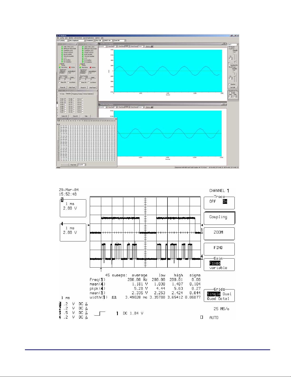
Results
Figure 6 shows a screenshot of the implemented
UART interface protocol. Shown are the initial
status message with the addresses of control
variables and two
Figure 7 shows a graphical visualization of the
output data in “pass-through” mode. Inputs are
generated externally (1 kHz sine waves) on a
subset of the 24 T1 channels. R
externally to S
the same data, only delayed in time.
Figure 8 shows an example of how the debugging
flag pins (PF1 and PF3) can be used to show, for
instance, the execution time for the processing of
all channels, or any other useful time in a
relatively straightforward way. The example was
taken from an application where the algorithm
was a line echo canceller (128 ms tail length).
Each of the 32 channels is processed, although
channels 24-31 are not used by a T1 connection.
write_mem commands.
is looped back
OUT
, such that all four streams contain
IN
This was solely intended to demonstrate that the
processing power of the Blackfin processor is
sufficient to do significant amounts of calculations
on all 32 channels, and leaving about 27% of the
total time for other tasks, such as the UART
interface.
Conclusions
This EE-Note, along with schematic drawings and
software framework provides design ideas for a
variety of T1/E1 communication lines.
The main focus is to interface the Blackfin
processors’ serial ports to standard backplane
formats and to show how to process the PCM
data. This is demonstrated on PCM streams from a
framer device such as the PM4351.
Interfacing T1/E1 Transceivers/Framers to Blackfin® Processors via the Serial Port (EE-234) Page 11 of 13
Page 12
a
Figure 7. R
and S
OUT
S
is looped back externally from R
IN
(channel 0) in “pass-through” mode (RIN is a 1kHz sine-wave for channels 0,1 and 2),
OUT
OUT
.
Figure 8. Execution time (signal PF1, trace 1) and individual channel convergence indicator (signal PF3, trace 4)
in the case of a line echo canceller algorithm. See RESULTS section for more details
Interfacing T1/E1 Transceivers/Framers to Blackfin® Processors via the Serial Port (EE-234) Page 12 of 13
Page 13

a
References
[1] ADSP-BF531/ADSP-BF532/ADSP-BF533 Blackfin Embedded Processor Data Sheet. Rev 0, March 2004.
Analog Devices, Inc.
[2] ADSP-BF533 Blackfin Processor Hardware Reference Manual. Revision 1.0, December 2003.
Analog Devices, Inc.
[3] ADSP-BF561 Blackfin Processor Hardware Reference Manual. Preliminary Revision 0.2, November 2003.
Analog Devices, Inc.
[4] PM4351 COMET Combined E1/T1 Transceiver Datasheet. Issue10, November 2000. PMC-Sierra, Inc.
[5] PM4351 COMET Combined E1/T1/J1 Transceiver/Framer Device Errata. Issue6, April 2002.
PMC-Sierra, Inc.
[6] PM4351 COMET Reference Design. Rev. 2.0, Issue1, November 1998. PMC-Sierra, Inc.
[7] PM4351 COMET Programmer’s Guide. Issue2, September 2000. PMC-Sierra, Inc.
[8] Lex and Yacc for Embedded Programmers. Embedded Systems Programming.
http://www.embedded.com/story/OEG20030220S0036
Document History
Revision Description
Rev 1 – May 11, 2004
by K. Unterkofler
Initial Release
Interfacing T1/E1 Transceivers/Framers to Blackfin® Processors via the Serial Port (EE-234) Page 13 of 13
 Loading...