

Page 1

Engineer-to-Engineer Note EE-200
a
Technical notes on using Analog Devices DSPs, processors and development tools
Contact our technical support at dsp.support@analog.com and at dsptools.support@analog.com
Or vi sit our o n-li ne r esou rces htt p:/ /www.analog.com/ee-notes and http://www.analog.com/processors
ADSP-TS20x TigerSHARC® Processor Boot Loader Kernels Operation
Contributed by B. Lerner Rev 1 – March 4, 2004
Introduction
This EE-Note explains the functional operation
of the power-on booting procedure and the boot
loader kernels for the ADSP-TS20x
TigerSHARC® family of processors.
This EE-Note focuses on kernels for ADSPTS201S and ADSP-TS202S processors. Kernels
for ADSP-TS203S processors form a subset of
the discussed functionality because this
processor has only two link ports and a 32-bit
external bus. Except for these restrictions, the
following information applies to all ADSPTS20x processors.
Loader Kernels and Boot Modes
A loader kernel is a program executed by the
processor that is appended to user application
code by the elfloader utility (
VisualDSP++® development tools. The
processor executes the loader kernel processor at
boot time, allowing the processor to initialize its
internal and external memory sections defined in
the application code.
The loader kernel is a self-modifying program
that is transferred into the processor’s internal
memory. The ADSP-TS20x family of processors
supports three booting methods: EPROM booting
(via the external port), host booting (via an
external host processor or another ADSP-TS20x
processor), and link booting (via the processor’s
link ports). VisualDSP++ includes three distinct
loader kernels that support each of the
elfloader.exe) of the
processor’s booting modes. Additionally, there
are several no-boot modes, which do not require
kernels.
Booting Procedure
The booting mode is selected by the processor's
/BMS pin. While the processor is held in reset, the
/BMS pin is an active input. If /BMS is sampled
low a certain number of SCLK cycles after reset,
EPROM boot mode is selected; a number of
SCLK cycles after this, the
output and serves as the EPROM chip select. If
/BMS is sampled high instead, the ADSP-TS20x
processor will be in an idle state, waiting for a
host boot or a link port boot to occur. The exact
timing for sampling
following driving of
processor's data sheet [3].
Additionally, a weak internal pull-down resistor
is on the
/BMS pin. Depending upon the external
line loading on this pin, this pull-down resistor
may not be sufficient,. Thus, you may need to
add an external pull-down resistor to select
EPROM booting mode. If host or link boot is
desired,
/BMS must be held high during and after
reset and may be tied directly to
provided it is never used as a chip select.
Each booting method is described in detail in the
following sections.
/BMS pin becomes an
/BMS boot strap and
/BMS is provided in the
VDD_IO,
Copyright 2004, Analog Devices, Inc. All rights reserved. Analog Devices assumes no responsibility for customer product design or the use or application of
customers’ products or for any infringements of patents or rights of others which may result from Analog Devices assistance. All trademarks and logos are property
of their respective holders. Information furnished by Analog Devices applications and development tools engineers is believed to be accurate and reliable, however
no responsibility is assumed by Analog Devices regarding technical accuracy and topicality of the content provided in Analog Devices’ Engineer-to-Engineer Notes.
Page 2
a
EPROM Boot
When EPROM boot mode is selected, the ADSPTS20x processor initializes its external port
DMA channel 0 to transfer 256 32-bit words of
code from the boot EPROM into memory block 0
locations 0x00-0xFF of the ADSP-TS20x
processor. The corresponding interrupt vector
(for DMA channel 0) is initialized to 0. Upon
completion of the DMA, the ADSP-TS20x
processor continues program execution from
location 0x00. These 256 words of code act as a
boot loader to initialize the rest of the ADSPTS20x processor’s memory. The VisualDSP++
development tools provide a default boot loader
kernel source file (
as a reference.
TS201_prom.asm), which serves
utility takes your project's executable file (
*.dxe)
and the boot loader executable file (default:
TS201_prom.dxe) and produces an EPROM loader
output file (
*.ldr). The loader output file specifies
how various blocks of ADSP-TS20x processor’s
internal and external memory are to be initialized
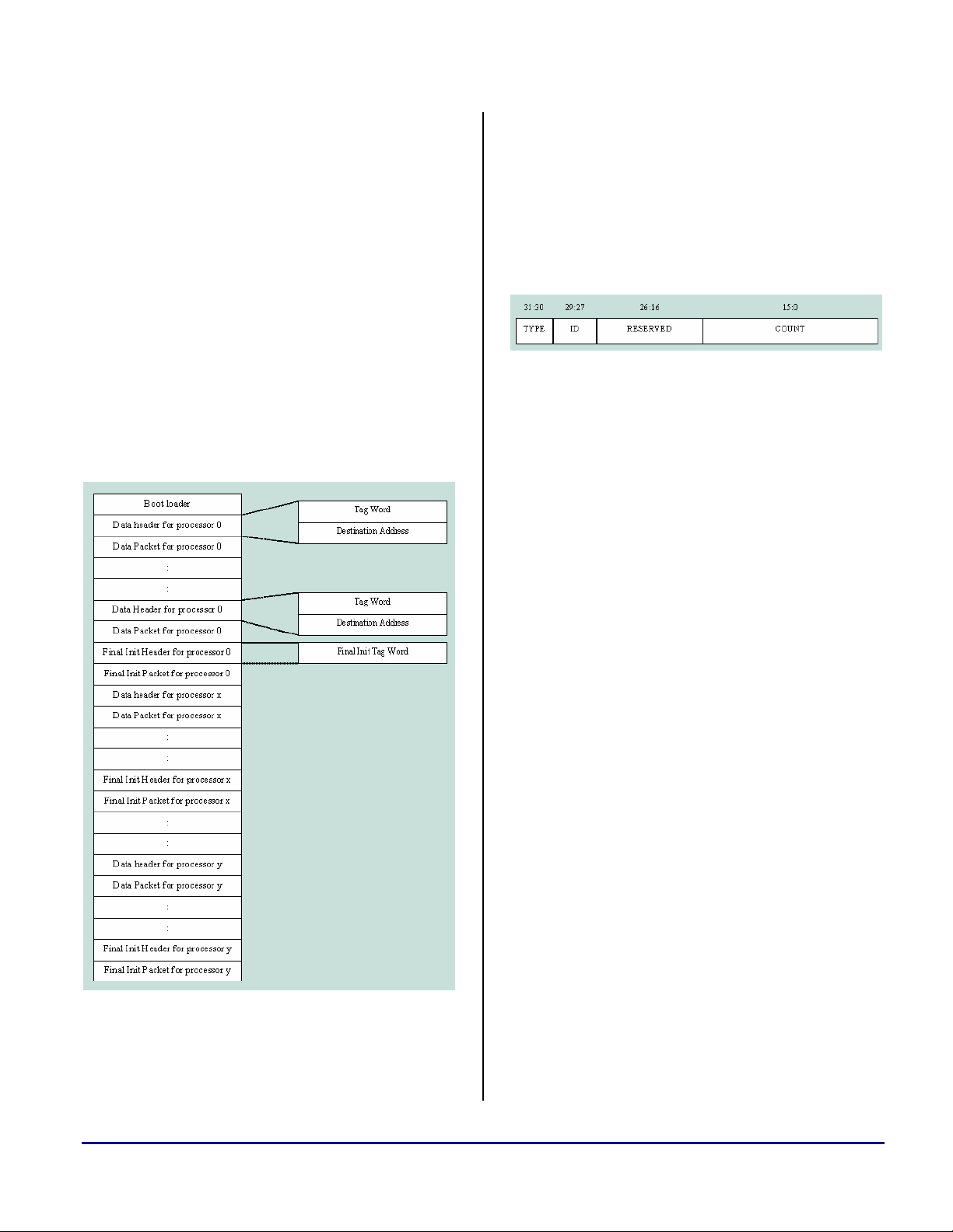
during the booting process. Figure 1 describes its
format. Figure 2 describes the block tag word.
Type: 0=Final init, 1=Non-zero init, 2=Zero init
ID: ID of the processor to which the block belongs
COUNT: Number of 32-bit words in the block
Figure 2: Block Tag Word Format
The supplied boot loader (TS201_prom.dxe)
operates as follows:
1. After the boot loader is loaded, the
DMA0
interrupt wakes up the ADSP-TS20x
processor and starts execution of the loader at
location 0x00000000. At this stage, the
ADSP-TS20x processor is at interrupt level
of
DMA0; further DMA0 and global
(
SQSTAT[20]) interrupts are disabled.
2. Note the code delimited by the labels
__init_debug_start and __init_debug_end. This
code describes the final state of some of the
processor's system registers after the loader
has finished booting all of the user code. The
simulator and the emulator use this code to
set these registers to the same state when a
.
DXE file is loaded (without having to run the
loader). The RDS function is important to the
loader's operation , because it reduces the
interrupt level of
DMA0 interrupts. Before RDS;; set the NMOD
bit in the
SQCTL register to ensure that the
DMA0 and allows further
processor remains in supervisor mode. Also,
Figure 1. EPROM Loader File Format
The default EPROM boot loader works in
conjunction with the loader utility (
elfloader.exe)
all link port DMAs are disabled. The real
loader code starts at label
__init_debug_end.
3. All cache is disabled. This is not necessary
for correct loader operation but it places the
supplied with the VisualDSP++ tools. The loader
ADSP-TS20x TigerSHARC® Processor Boot Loader Kernels Operation (EE-200) Page 2 of 10
Page 3

a
cache in a known clean state when the user
code takes over.
4. The loader sets the
bits in the
NMOD, TRCBEN, and GIE
SQCTL register, ensuring
supervisor mode and enabling trace buffer
and global interrupts.
5. The
DMA0 interrupt vector is set to dma_int.
DMA0 is set up to move data from boot
PROM starting at 0x0400 (0x0000-0x03ff
was the boot loader) to internal memory
starting at 0x00000000. The DMA routine
starts the DMA by programming the TCBs,
advancing the PROM pointer, and sitting in
idle until the DMA interrupt wakes it up and
sends it to dma_int. There,
RTI returns to the
DMA routine, which, in turn, returns to
loader execution.
6. Registers
xR1 contains the source count, and xR5
xR7:0 will be used to start DMA0.
contains the destination count, which will
vary (and modifies which are always one and
four); thus,
individually before starting
to the value of the source
EPROM/Priority=Norm/Normal Word/Interrupt=On.
xR7 is set to value of destination DP, which is
EPROM/Priority=Norm/Normal Word/Interrupt=On.
xR0 (i.e., source address) starts at
0x00000400 (incrementing as necessary).
xR1 and xR5 will be set
DMA0. xR3 is set
DP, which is
xR4
(i.e., destination address) is set to
0x00000000.
7. The processor ID is computed and stored in
xR10.
8. The loader parses the blocks of data from the
PROM. Two words (the tag words of the
block to follow) are moved to locations
0x00000000 and 0x00000001. . In the first
word, bits 31:30 are block
TYPE (0=final init,
1=non-zero init, 2=zero init), bits 29:27 are
the processor ID, bits 26:16 are reserved and
bits 15:0 are the block
tag word is pointer to
COUNT. The second
DESTINATION.
9. The ID of the block is compared to the ID
stored in
xR10. If the IDs are not the same,
the PROM block is skipped.
10. If the IDs are the same, the type is examined.
11. If type is 1, the
COUNT number of words is
moved one word at a time via location
0x00000000 to the
DESTINATION. Once
finished, the steps starting with 8 are
repeated.
12. If type is 2, the
moved to the
COUNT number of zeros is
DESTINATION. Once finished,
the steps starting with 8 are repeated.
13. If type is 0, the loader performs the final init
(i.e., it overwrites itself with the user code).
A DMA of 256 words into 0x000000000x000000ff with wake up from idle would do
this, but would start user code execution at
interrupt level of DMA0. To avoid this, the
following algorithm is used:
a. First four instructions of user code
(destined to locations 0x000000000x00000003) are DMAed from the
PROM and stored in registers
xR11:8.
b. The following code is written into
locations 0x00000000-0x00000003:
RETI = 0;;
SQCTL = yr0;;
RTI (ABS)(NP); Q[j31+=0] = xR11:8;;
c. The DMA0 interrupt vector is set to
0x00000000.
d.
yR0 is preset to SQCTL_NMOD |
SQCTL_TRCBEN
(this disables global
interrupts when the user code starts, but
ensures that the
mode) and
TRCBEN bit (trace buffer) are
NMOD bit (supervisor
enabled. This value will be written into
the
SQCTL register in the _last_patch_code
that was relocated to 0x000000000x00000003.
ADSP-TS20x TigerSHARC® Processor Boot Loader Kernels Operation (EE-200) Page 3 of 10
Page 4

a
e. The Branch Target Buffer is invalidated
(
BTBINV) to clear any possibly cached
branches.
f. Cache is re-enabled.
g. The DMA is set up to transfer 252 words
of user code destined to 0x00000004-
0x000000ff.
h. DMA is started by writing to the TCBs,
and then the processor goes idle.
i. When the DMA is finished, an interrupt
wakes up the ADSP-TS20x processor and
jumps execution to code inserted at
0x00000000 (See Step b).
j. This code executes
disables all global interrupts, then
(ABS) (NP); Q[j31+=0]=xR11:8;;, which
SQCTL = yR0;; which
RTI
reduces the interrupt level to none,
placing user code into locations
0x00000000-0x00000003 and jumping
execution to 0x00000000 (since
RETI is
set to 0x00000000). The user code starts
cleanly at 0x00000000, with no interrupt
level. Note that the
to prevent
RTI from caching into BTB.
NP option is necessary
If external memory (such as SDRAM) requires
special initialization, the boot loader kernel must
configure it. This memory configuration must
precede its initialization in the boot loader
kernel. Thus, you must modify and rebuild the
boot loader to the requirements of the application
and system.
Host Boot
When a host or link boot is selected, the ADSPTS20x processor enters an idle state after reset,
waiting for the external host processor or link
port to boot it. Host booting uses the ADSPTS20x processor’s AUTODMA registers (either
channel), both of which are initialized to transfer
256 words of code to block 0, locations 0x000xFF of the ADSP-TS20x processor’s internal
memory. The corresponding interrupt vector is
initialized to point to address 0x00. Thus, upon
completion of the DMA, the ADSP-TS20x
processor continues execution at memory
location 0x00. These 256 words of code act as a
boot loader to initialize the rest of the ADSPTS20x processor’s memory. The VisualDSP++
development tools supplies a default boot loader,
named
TS201_host.asm.
The default host boot loader works in
conjunction with the loader utility included with
the VisualDSP++ development tools. The loader
utility takes your project's executable file and the
boot loader executable (
produces the host loader file with an
TS201_host.dxe) and
.LDR
extension . The host loader file specifies how
various blocks of the ADSP-TS20x processor’s
internal and external memory segments are to be
initialized. Its format is described in Figure 1.
Format of the block tag word is described in
Figure 2.
In the following procedure, the
register can be replaced with the
AUTODMA0
AUTODMA1
register, making the appropriate changes to the
boot loader code to reflect this change in register
usage.
The supplied boot loader uses the
AUTODMA0
register and works as follows:
1. After the boot loader is loaded, the
AUTODMA0 interrupt wakes up the ADSP-
TS20x processor and starts the execution of
the host boot loader kernel at location
0x00000000. At this stage, the TigerSHARC
processor is at interrupt level of
and thus, further
interrupts (
SQSTAT[20]) are disabled. The
AUTODMA0 and global
AUTODMA0,
loader, as described below, parses subsequent
words sent by the host.
2. It is important for the loader to control when
the host can send new data to
AUTODMA0.
Although the processor will NACK all host
writes to
AUTODMA0 when the AUTODMA0
buffer is full, it ignores writes to AUTODMA0
when AUTODMA0 is disabled, so any data
written when
AUTODMA0 is disabled simply
ADSP-TS20x TigerSHARC® Processor Boot Loader Kernels Operation (EE-200) Page 4 of 10
Page 5

a
falls through. For this reason, the loader uses
BUSLK to lock the bus while processing new
data and until the data is processed and the
AUTODMA0 is re-enabled. Important
guidelines that the host must follow to ensure
proper boot follow this description of the
loader algorithm.
3. Note the code delimited by the labels
__init_debug_start and __init_debug_end. This
code specifies the final state of some of the
processor's system registers after the loader
has finished booting all of the user code. The
simulator and the emulator use this code to
set the registers to the same state when a
DXE
file is loaded (this bypasses having to run the
loader). The
RDS function is important to the
loader operation of the loader as it reduces
the interrupt level of
DMA0 interrupts. Before RDS;; it is very
important to set the
DMA0, allowing further
NMOD bit in the SQCTL
register to ensure that the processor remains
in supervisor mode. Also, all link port DMAs
are disabled. The real loader code starts at
label
__init_debug_end.
4. All cache is disabled. This is not necessary
for the correct loader operation but is
performed to place cache in a known clean
state when the user code takes over.
5. The loader sets the
bits in the
NMOD, TRCBEN, and GIE
SQCTL register, ensuring
supervisor mode and enabling trace buffer
and global interrupts.
6. The
AUTODMA0 interrupt vector is set to
_dma_int.
7. The processor ID is computed and stored in
xR10.
8. Registers
AUTODMA0. xR1 contains the count, which
xR3:0 will be used to start
will vary (and modify which is always one);
thus,
starting
DP, which is Internal Memory/Priority=
xR1 will be set individually before
AUTODMA0. xR3 is set to the value of
High/Normal Word/Interrupt=On.
xR0 (i.e.,
destination) is set to 0x00000000.
9. The loader parses the blocks of data from the
host. It sets up to transfer two words (the tag
words of the block to follow). In the first
word, bits 31:30 are block
TYPE (0=final init,
1=non-zero init, 2=zero init), bits 29:27 are
the processor ID, bits 26:16 are reserved, and
bits 15:0 are the block
tag word is a pointer to
COUNT. The second
DESTINATION.
10. The ID of the block is compared to the ID
stored in
the block is skipped (if
getting 255 or
xR10. If the IDs are not the same,
TYPE=0 or 1, by
COUNT number of words from
the host without any store) and steps starting
with 9 are repeated.
11. If the IDs are the same, the type is examined.
12. If type is 1, the
COUNT number of words is
moved one word at a time via AUTODMA0
to the
DESTINATION. Once finished, the steps
starting with 9 are repeated.
13. If type is 2, the
moved to the
COUNT number of zeros is
DESTINATION. Once finished,
the steps starting with 9 are repeated.
14. If type is 0, the loader performs the final init
(i.e., it overwrites itself with the user code).
An
AUTODMA0 of 256 words into
0x00000000-0x000000ff with wake up from
IDLE would do this, but would start user code
execution at the interrupt level of
AUTODMA0. To avoid this, the following
algorithm is used:
a. The first four instructions of user code
(for locations 0x00000000-0x00000003)
are AUTODMAed from the host and
stored in registers
xR11:8.
b. The following code is written into
locations 0x00000000-0x00000003:
RETI = 0;;
SQCTL = yR0;;
RTI (ABS) (NP); Q[j31+=0] = xR11:8;;
ADSP-TS20x TigerSHARC® Processor Boot Loader Kernels Operation (EE-200) Page 5 of 10
Page 6

a
c. The AUTODMA0 interrupt vector is set to
0x00000000.
d.
yR0 is preset to SQCTL_NMOD |
SQCTL_TRCBEN
(to leave global
interrupts disabled when the user code
starts, but to ensure that the
(supervisor mode) and the
NMOD bit
TRCBEN bit
(trace buffer) are enabled. This value will
be written into the
SQCTL register in the
_last_patch_code that was relocated to
0x00000000-0x00000003.
e. The Branch Target Buffer is invalidated
(
BTBINV) to clear any possibly cached
branches.
f. Cache is re-enabled.
g.
AUTODMA0 is set up to transfer 252
words of user code destined to
0x00000004-0x000000ff.
h.
AUTODMA0 is started by writing to the
TCBs. Bus lock is released and then the
processor goes idle.
i. When
AUTODMA0 is finished, an interrupt
wakes up the TigerSHARC processor and
jumps execution to code inserted at
0x00000000 (See Step b).
j. The code executes
disables all global interrupts, then
(ABS) (NP); Q[j31+=0]=xR11:8;;,
SQCTL = yR0;; which
RTI
which
reduces the interrupt level to none,
placing user code into locations
0x00000000-0x00000003 and jumping
execution to 0x00000000 (since
RETI is
set to 0x00000000). The user code starts
cleanly at 0x00000000 with no interrupt
level. Note that the
to prevent
RTI from caching into BTB.
NP option is necessary
If external memory (such as SDRAM) requires
special initialization, the boot loader kernel must
configure it. This memory configuration must
precede its initialization in the boot loader
kernel. Thus, the boot loader must be modified
and rebuilt to the requirements of your specific
application and system.
Important Host Guidelines
Observe the following guidelines.
1. After the processor's
receives the data, a delay of up to 12
cycles occurs before the
AUTODMA0 register
CCLK
AUTODMA0
register's ISR is serviced and bus lock is
enabled. Data sent to
AUTODMA0 during this
time will be lost. Thus, the host must insert
waits of at least 12*
between each write to the
SCLKRAT external cycles
AUTODMA0
register of the slave DSP to ensure proper
boot.
2. If the host has an external port output FIFO
(for example, when the host is another
ADSP-TS20x processor), delayed writes to
the external port may not guarantee the same
delay between the times when these
transactions take place on the external port. If
this output FIFO has several transactions
queued into it, when the slave DSP releases
bus lock, all of the queued transactions will
come out back-to-back, thus violating the
guideline above. Special care may be needed
to handle this issue. If, for example, the host
is another ADSP-TS20x processor, inserting
reads of any dummy address on the external
bus between all writes to
AUTODMA0 with a
dependency on the read value will
automatically stall until the read is finished,
thus the write that follows after the dummy
read will not be queued into the FIFO until
the first write and read are finished.
Following is an example ADSP-TS20x processor
host code:
// Write to AUTODMA0 of processor ID=2
[j31+(P2_OFFSET_LOC+AUTODMA0_LOC)]=xr0;;
// delay the required number of cycles
call delay_12_times_sclkrat_cycles;;
// read external dummy memory location
ADSP-TS20x TigerSHARC® Processor Boot Loader Kernels Operation (EE-200) Page 6 of 10
Page 7

xr1=[j31+dummy_external_memory];;
// insert dependency before next write
xr1=xr1;;
.....
// Write to AUTODMA0 of processor ID=2
[j31+(P2_OFFSET_LOC+AUTODMA0_LOC)]=xr0;;
An example code of a ADSP-TS20x processor
acting as a master, host booting another ADSPTS20x processor is provided with the examples
for the ADSP-TS201S EZ-KIT Lite™
development system.
Link Boot
When a host or link boot is selected, the ADSPTS20x processor enters an idle state after reset,
waiting for the host or link port to boot it. A link
boot can use any of the ADSP-TS20x processor’s
link ports, all of whose DMAs are initialized to
transfer 256 words of code to ADSP-TS20x
processor’s memory block 0, locations 0x000xFF. The corresponding DMA interrupt vectors
are initialized to 0. Thus, upon completion of the
link DMA, the ADSP-TS20x processor continues
execution at location 0x00. These 256 words of
code act as a boot loader to initialize the rest of
ADSP-TS20x processor’s memory. Analog
Devices supplies a default boot loader,
TS201_link.asm, with the VisualDSP++ tools set.
The default link boot loader works in
conjunction with the loader utility supplied with
VisualDSP++. The loader utility takes your
project's executable file (
loader executable file, (default:
and produces the loader output file (
.
LDR file specifies how various blocks of ADSP-
TS20x processor’s internal and external memory
are to be initialized. Its format is described in
Figure 1. Format of the block tag word is
described in Figure 2.
The supplied boot loader works as follows:
1. After the boot loader is loaded, the link port
DMA interrupt wakes up the TigerSHARC
*.DXE) and the boot
TS201_link.dxe)
*.LDR). The
a
processor and starts the execution of the
loader at location 0x00000000. At this stage,
the TigerSHARC processor is at the interrupt
level of the link DMA, and further link port
DMAs and global (
SQSTAT[20]) interrupts are
disabled.
2. The LINK constant specifies the link port to
be used for booting. It is set to 3 (i.e., link
port 3) in this code. If a different link port is
used, modify the value and rebuild the code .
3. Note the code delimited by the labels
__init_debug_start and __init_debug_end. This
code specifies the final state of some of the
processor's system registers after the loader
has finished booting all of the user code. The
simulator and the emulator use this code to
set these registers to the same state when a
.
DXE file is loaded (this bypasses having to
run the loader). The
RDS function is
important to the operation of the loader as it
reduces the interrupt level of
allowing further
Before
NMOD bit in the SQCTL register to ensure that
RDS;; it is very important to set the
AUTODMA0 interrupts.
AUTODMA0,
the processor remains in supervisor mode.
Also, all link port DMAs are disabled. The
real loader code starts at label
__init_debug_end.
4. All cache is disabled. This is not necessary
for the correct loader operation but is
performed to place cache in a known clean
state when the user code takes over.
5. The loader sets the
bits in the
NMOD, TRCBEN, and GIE
SQCTL register, ensuring
supervisor mode and enabling trace buffer
and global interrupts.
6. The link port receive DMA interrupt vector is
set to
_dma_int. Unused link ports are cleared
and disabled. Link port DMAs are disabled.
7. The link port control registers are initialized.
8. The DMA to bring in data from the link port
will do this one quad word at a time.
XR3:0
ADSP-TS20x TigerSHARC® Processor Boot Loader Kernels Operation (EE-200) Page 7 of 10
Page 8

a
are preset with the required values for the
TCB.
9. Data from the link is read by the
_read_word
routine. Since data from link is in quad
format and the processor parses it in single
32-bit words, an internal FIFO buffer is
maintained. This is implemented as a circular
buffer in memory locations 0x00-0x03.
J2 is
dedicated as the read pointer to the buffer,
and
accordingly. The execution flow of
J2, JB2, and JL2 are initialized
_read_word
is:
a.
J2 is checked to determine whether it has
wrapped back to 0 (i.e., all the data in the
buffer has been read). If it has not, go to
"step d" to read the next piece of data
from the buffer.
b. Another quad word is brought into the
buffer from the link port via link DMA.
Link port DMA is started by writing
XR3:0 to the TCB, and the routine waits
for the DMA interrupt in
IDLE.
c. When the new quad word arrives from
the link port, DMA interrupt wakes up
the processor from
branched to
NOPs followed by RTI;; returns it back to
one instruction past the
the line of
NOPs is necessary here, RTI;; is
IDLE and execution is
_dma_int, where a line of
IDLE. Note that
not allowed to be in the first quad of an
ISR.
d. Data from the buffer pointed to by
read into
xR4, and J2 is incremented
J2 is
circularly.
10. Unlike other boot modes, the processor ID is
not used. The loader does not support the MP
boot.
11. The loader parses the blocks of data from the
link port. Two words (the tag words of the
block to follow) are moved to
the first word, bits 31:30 are block
yR8 and J0. . In
TYPE
(0=final init, 1=non-zero init, 2=zero init),
bits 29:16 are reserved, and bits 15:0 are the
block
pointer to
12. If type is 1,
moved one word at a time via
the
COUNT. The second tag word is the
DESTINATION.
COUNT number of words is
_read_word to
DESTINATION. Once finished, the
algorithm goes to Step 11.
13. If type is 2, the
moved to the
COUNT number of zeros is
DESTINATION. Once finished,
the algorithm goes to Step 11.
14. If type is 0, the loader performs the final init
(i.e., it overwrites itself with the user code).
The following algorithm is used:
a. The first 28 instructions of user code
(destined to locations 0x000000000x0000001B) are moved from the link
port via
xR31:8 and yR31:28 registers.
_read_word and stored in the
b. The interrupt service routine at _dma_int
is relocated to 0x04-0x08.
c. 19 instructions of
_last_patch_code are
relocated to locations 0x09-0x1B.
d. The Branch Target Buffer is invalidated
(
BTBINV) to clear cached branches.
e. Cache is re-enabled.
f. The link port DMA interrupt vector is set
to 0x04 (the location that now contains
the interrupt service routine as a result of
Step b).
g. yR0 is preset to
SQCTL_TRCBEN
SQCTL_NMOD |
(this leaves global
interrupts disabled when the user code
starts), ensuring that the
(supervisor mode) and the
NMOD bit
TRCBEN bit
(trace buffer) are enabled. This value will
be written into the
_last_patch_code that was relocated to
SQCTL register in the
0x00000000-0x0000001B.
h.
J0 is initialized to 0x1C (first location
past relocated
_last_patch_code), and LC0 is
initialized to 0xE4 (number of words left
in the final init to be read).
ADSP-TS20x TigerSHARC® Processor Boot Loader Kernels Operation (EE-200) Page 8 of 10
Page 9

i. At this stage, locations 0x04-0x1B are
initialized as follows:
0x04: _relocated_dma_int:
nop; nop; nop; nop;;
rti(NP);;
0x09: _relocated_read_word:
// if J2 -> start of the buffer...
comp(j2,0);;
// ...bring in more data
if njeq, jump _relocated_read_buffer
(NP);;
// start the DMA
DCx = xr3:0;;
// wait till DMA interrupts
idle;;
_relocated_read_buffer:
// read the word from the buffer
xr4 = cb[j2+=1];;
// and return
cjmp (ABS) (NP);;
0x0F: _relocated_final_init1:
// read word
call _read_word (NP);;
// write it
[j0 += 1] = xr4;;
if NLC0E, jump _relocated_final_init1
(NP);;
// disable interrupts
SQCTL = yr0;;
nop;;
// overwrite 0x00-0x03
Q[j31 + 0] = xr11:8;;
// overwrite 0x04-0x07
Q[j31 + 4] = xr15:12;;
// overwrite 0x08-0x0b
Q[j31 + 8] = xr19:16;;
// overwrite 0x0c-0x0f
Q[j31 + 0xc] = xr23:20;;
// overwrite 0x10-0x13
Q[j31 + 0x10] = xr27:24;;
// overwrite 0x14-0x17
Q[j31 + 0x14] = xr31:28;;
// overwrite 0x18-0x1b, start at 0
jump 0(ABS)(NP);Q[j31+0x18]=yr31:28;;
a
j. The code execution jumps to 0x0F (i.e.,
_relocated_final_init1 shown above).
k. Locations 0x1C-0xFF are filled with
data from the link port. Note that call
_read_word (NP);; at _relocated_final_init1
is a relative call. Thus, it actually
calls
overwriting old
_relocated_read_word, and
_read_word does not
cause any problems.
l. Now link receiving is finished. The
correct data is in 0x1C-0xFF, and the data
that should be in 0x00-0x1B is in
registers
xR31:8 and yR31:28. The
remaining code overwrites memory
location 0x00-0x17 with the data in
xR31:8, and finally, the last line of code
overwrites locations 0x18-0x1B
(including itself) with data from
while executing an absolute jump to
0x00.
m. The user code starts at 0x00 cleanly.
If external memory (such as SDRAM) that
requires special setup needs to be initialized by
the loader, that memory’s setup has to precede its
initialization in the boot loader. Thus, the boot
loader has to be modified by the user and rebuilt.
No Boot
When a host or link boot is selected, the ADSPTS20x processor enters an idle state after reset,
waiting for the host or link port to boot it. It does
not have to be booted by the host or a link port.
If external interrupts
at reset by the IRQEN strap pin), they can be
IRQ3:0 are enabled (selected
yR31:28
ADSP-TS20x TigerSHARC® Processor Boot Loader Kernels Operation (EE-200) Page 9 of 10
Page 10

a
used to force code execution according to the
default interrupt vectors, as shown in Table 1.
In this scenario, another device, such as a host
processor, initializes the appropriate memory
with the appropriate code and then forces the
corresponding IRQx.
Interrupt Address
IRQ0 0x30000000 (MS0)
IRQ1 0x38000000 (MS1)
IRQ2 0x80000000 (MSH)
IRQ3 0x00000000 (Internal Memory)
Table 1. IRQ3:0 Default Interrupt Vectors
Another no-boot method of starting up the
ADSP-TS20x processor is for a host to initialize
a memory buffer with code and then force that
code execution via a vector interrupt.
No-boot methods are useful for system debug,
but are not recommended for production. Many
intricate details must be addressed when the chip
is started up. The standard supplied loaders take
care of those details, so system start up based on
those loaders is highly recommended.
References
[1] ADSP-TS201 TigerSHARC Processor Hardware Reference. Revision 1.0, May 2003. Analog Devices, Inc.
[2] ADSP-TS201 TigerSHARC Processor Programming Reference. Revision 0.1, June 2003. Analog Devices, Inc.
ADSP-TS201S TigerSHARC Embedded Processor Preliminary Data Sheet. Rev PrH, January 2004.
[3]
Analog Devices, Inc.
Document History
Revision Description
Rev 1 – March 04, 2004
by B. Lerner
Initial Release
ADSP-TS20x TigerSHARC® Processor Boot Loader Kernels Operation (EE-200) Page 10 of 10
 Loading...