

Page 1
Engineer To Engineer Note EE-196
a
Technical Notes on using Analog Devices' DSP components and development tools
Contact our technical support by phone: (800) ANALOG-D or e-mail: dsp.support@analog.com
Or vi sit ou r on-l ine re sourc es ht tp:// www.analog.com/dsp and http://www.analog.com/dsp/EZAnswer
ADSP-BF535 Blackfin® EZ-KIT Lite™ CompactFlash® Interface
Contributed by Hiren Desai June 4, 2003
Introduction
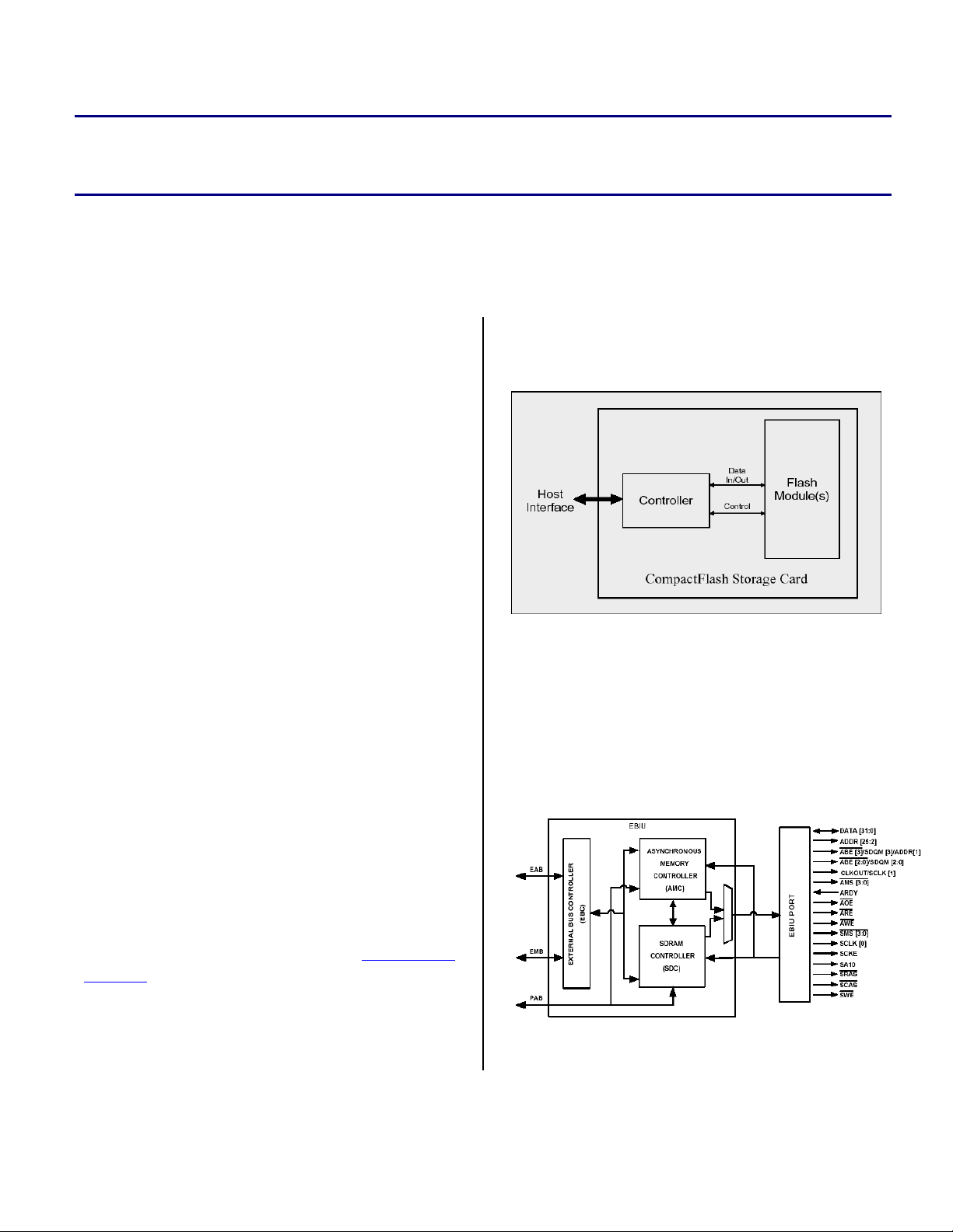
CompactFlash® storage cards provide the
capability to easily transfer/store all types of
digital information, such as data, audio, and
images, between large varieties of digital
systems. CompactFlash cards are high density
(up to 1Gbytes of nonvolatile storage memory!),
removable (i.e. hot-swappable), and very
compact in size. CF™ cards can be used as
memory storage devices for digital imaging,
video, audio, PDAs, etc. but they can also be
extended for I/O communications applications
such as modems, Ethernet controllers, laser
scanners, BlueTooth Wireless, 802.11 WiFi
LAN, wireless digital cell phone cards, and GPS
nodes.
This note describes one way to interface a
CompactFlash Storage Card to the ADSP-BF535
EZ-KIT Lite™ Evaluation Board. The interface
consists of a hardware and software
implementation, both of which will be discussed
in this application note. In this example, the
interface will demonstrate the playing of MP3
tracks (stored on the CompactFlash card) by the
ADSP-BF535 Blackfin® processor.
configured/formatted by a Windows host PC, it
appears to the host as a standard ATA (IDE) disk
drive.
Figure 1. CompactFlash Storage Card Block
Diagram
Because of this, CompactFlash cards can be
easily interfaced to the ADSP-BF535 Blackfiin
processor’s Asynchronous Memory through the
External Bus Interface Unit (EBIU). The EBIU
provides glueless interfaces to external
memories.
s
Overview
CompactFlash Cards conform to the CF and CF+
standard published by the CompactFlash
Association (CFA). There is an on-card
intelligent controller that manages interface
protocols, data storage and retrieval (see Figure
Figure 2. External Bus Interface Unit (EBIU)
1). Once the CompactFlash card has been
Copyright 2003, Analog Devices, Inc. All rights reserved. Analog Devices assumes no responsibility for customer product design or the use or application of
customers’ products or for any infringements of patents or rights of others which may result from Analog Devices assistance. All trademarks and logos are property
of their respective holders. Information furnished by Analog Devices Applications and Development Tools Engineers is believed to be accurate and reliable, however
no responsibility is assumed by Analog Devices regarding technical accuracy and topicality of the content provided in Analog Devices’ Engineer-to-Engineer Notes.
Page 2
a
]
]
]
[1]
]
[0]
[
]
The EBIU is clocked by the system clock
(SCLK) of the ADSP-BF535 Blackfin processor.
On the ADSP-BF535 Blackfin EZ-KIT Lite,
SCLK is set to 120MHz, which will be more
than sufficient for accesses to CompactFlash
cards. Read/Write access times on
CompactFlash cards are defined between 250ns –
300ns (~ 3 – 4 MHz). To find interface/bus
timing, please refer to the CF/CF+ standard
.
CompactFlash cards function in three basic
modes:
• PC Card ATA using Common Memory Mode.
• PC Card ATA using I/O Mode.
• True IDE Mode.
This EE-Note will only deal with 16 bit transfers
using Common Memory Mode.
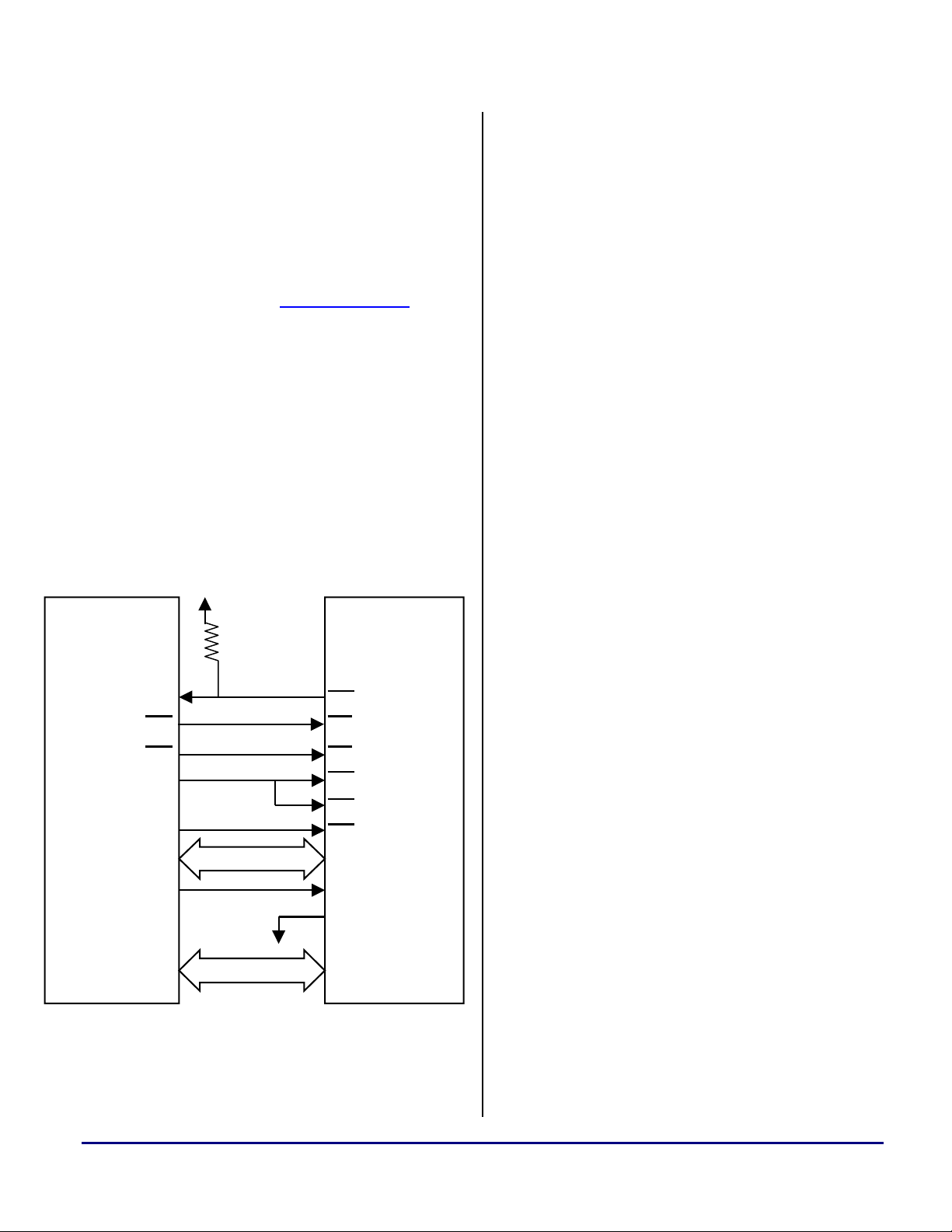
ADSP-BF535 CompactFlash Interface Pin Mapping
ADSP-BF535
PF8 CD1
AOE OE
AWE
AMS[1
A[11
A[10:2
D[15:0
Vcc
10 kOhm
Address Bus
GND
Data Bus
CompactFlash
WE
CE2
REG
A[10:2]
A
ABE[3] / A[1
A
D
15:0]
CompactFlash Signal Descriptions – Common
Memory Mode
• A[10:1]: Address Lines
• D[15:0]: Data Lines
• /WE (Write Enable): This signal is driven by
the ADSP-BF535 and used for strobing
memory write data to the registers of the
CompactFlash.
• /OE (Output Enable): This strobe is generated
by the ADSP-BF535 and used to read data
from the CompactFlash.
• REG (Attribute Memory Select): This signal
is to distinguish between Common Memory
and Register (Attribute) Memory accesses.
High for Common Memory, Low for Attribute
Memory.
• /CE1, /CE2 (Card Enable): These signals are
used both to select the card and to indicate to
the card whether a byte or a word operation is
being performed. Since both of these signals
are tied to AMS[1] of the ADSP-BF535, we
will be doing word (16-bit) accesses only.
• /CD1 (Card Detect): This signal is used by
the ADSP-BF535 to determine that the
CompactFlash is fully inserted into its socket.
• A[0]: Address line 0 is connected to ground
since this interface supports word accesses
only.
Software Implementation
Since we are using the CompactFlash as a PC
card ATA using memory mode, it will be seen by
the ADSP-BF535 as a standard ATA disk drive.
The following gives a brief explanation of the
file system used on standard disk drives.
Figure 3: CF Interface Pin Mapping
Figure 3 shows the main pin-to-pin connections
between the ADSP-BF535 and the CompactFlash
card.
ADSP-BF535 Blackfin® EZ-KIT Lite™ CompactFlash® Interface (EE-196) Page 2 of 15
FAT file system
Standard disk drives use the FAT (File
Allocation Table) file system. Currently there
are three types of FAT file systems: FAT12,
FAT16, and FAT32. In a FATnn file system, nn
Page 3

a
represents the size, in bits, of the entries in the
actual FAT structure on the disk. There are 12
bits in a FAT12 FAT entry, 16 bits in a FAT16
FAT entry and 32 bits in a FAT32 FAT entry.
Currently, this interface supports FAT16 only
but other FAT systems could be implemented.
There are 4 basic regions on a FAT volume:
• Reserved Region
• FAT Region
• Root Directory Region (non FAT32)
• File and Directory Data Region
Disk Structure Sector Offset
Boot Sector 0
FAT 1 1
FAT 2 (# of Sectors per FAT) + 1
Name
JumpBoot 3 Jump Instruction to boot
OEMName 8 Name string – MSWIN4.1.
BytesPerSector 2
SectorsPerCluster 1 1, 2, 4, 8, 16, 32, 64, 128.
ReservedSectors 2 1 for FAT12 and FAT16.
FATCount 1 2 FAT data structures.
RootEntCount 2 # of 32-byte entries in root
TotalSectors1 2 Total # of sectors on volume
MediaDescriptor 1 0xF8 for fixed media. 0xF0
SectorsPerFAT 2 # of sectors in one FAT.
SectorsPerTrack 2 Tracks are broken down into
Size
(in
bytes)
Description
code.
, 1024, 2048, 4096.
512
directory.
Bits[15:0].
for removable media.
heads and cylinders.
Root Directory 2*(# of Sectors per FAT)+1
File Clusters (Data
Region)
Table 2. Disk Structure
2*(# of Sectors per FAT)+1+(# of
Root Directory Sectors)
Reserved Region
The Reserved Region contains the Boot Sector
which is the first sector of the volume. A
summary of the FAT16 structure of the Boot
Sector is provide below, starting with the first
word at byte offset 0 (also applies to FAT12):
The Boot Sector contains all the information
about the physical structure of the
CompactFlash. This information is needed to
determine where data is stored on the
CompactFlash for retrieval.
HeadCount 2 Relevant for previous field.
HiddenSectors 4 Count of hidden sectors
preceding FAT volume.
TotalSectors2 4 Total # of sectors on volume
Bits[47:16].
DriveNumber 1 This field is OS specific.
Reserved 1 Reserved.
BootSignature 1 Extended Boot Sig. (0x29).
VolumeID 4 Volume serial number.
VolumeLabel 11 Volume label.
Reserved 8 Reserved.
Table 3. Boot Sector
FAT Region
There are two FAT data structures on the
volume. The reason there are two is to provide
redundancy for the FAT data structure so that if a
sector goes bad in one of the FATs, the data is
not lost because it is duplicated in the other FAT.
Each FAT is a single linked list of the clusters of
a file. These clusters map to the data region of
ADSP-BF535 Blackfin® EZ-KIT Lite™ CompactFlash® Interface (EE-196) Page 3 of 15
Page 4
a
the volume. The first 2 entries in the FAT are
reserved so logical cluster numbers begin at 2.
FAT16 Table
O
f
f
0
1
2
3
4
5
… ………
N-1 0012
N FFFF
Figure 4. FAT File System
Entry
(Next
Cluster)
FFF8
FFFF
0003
0004
000A
0008
(EOF)
Data Region
FAT16 entry values:
• 0x0000: Unused Cluster
• 0xFFF0 – 0xFFF6: Reserved Cluster
Root Directory
The Root Directory is composed of a linear list
of 32-byte structures which represent files stored
on the disk. The following table describes the
different fields of a 32-byte structure within the
Root directory:
Name Size
(in
bytes
)
Name 11 Short name. (see note below)
Attr 1 Bit 0: READ_ONLY
NTRes 1 Reserved for Windows NT use.
CrtTimeTenth 1 File creation time. Millisecond
CrtTime 2 File creation time. 2 second
CrtDate 2 File creation date.
LstAccDate 2 Last read/write date of file.
Description
Bit 1: HIDDEN
Bit 2: SYSTEM
Bit 3: VOLUME_ID
Bit 4: DIRECTORY
Bit 5: ARCHIVE
Bit 6: LONG_NAME
Bits 7 and 8: RESERVED
granularity.
granularity.
• 0xFFF7: Bad Cluster
• 0xFFF8 – 0xFFFF: End of Cluster/File
• Other: Next Cluster in File
The first sector is of cluster 2 and is calculated
as:
FirstDataSector = ReservedSectors + (FATCount *
SectorsPerFAT) + RootDirSectors
FstClusHI 2 File’s first cluster number;
bits[31:16]. This is 0 for
FAT12 and FAT16 volume.
WrtTime 2 Time of last write.
WrtDate 2 Date of last write.
FstClusLO 2 File’s first cluster number;
bits[15:0].
FileSize 4 File size in bytes.
Where
RootDirSectors = ((RootEntCount * 32) + (BytesPerSector
– 1)) / BytesPerSector
The first sector of any cluster N is calculated as:
FirstSectorofCluster = ((N – 2) * SectorsPerCluster) +
FirstDataSector
Table 4. 32-Byte Directory Entry Structure.
Note, if the first byte of the Name field =
• 0xE5: then the entry is free.
• 0x00: then the entry is free; there are no
more allocated entries after this one.
• Values less than 0x20: Not Valid (except
0x05 Å used in Japan).
ADSP-BF535 Blackfin® EZ-KIT Lite™ CompactFlash® Interface (EE-196) Page 4 of 15
Page 5

a
Long file names are not supported in this
software interface.
For FAT32 file systems, the root directory can be
of variable size and is a cluster chain.
For FAT12 and FAT16 file systems, the root
directory immediately follows the last FAT and
has a fixed location and fixed size on the disk.
The first sector of the Root Directory is
computed as:
FirstRootDirSec = ReservedSectors + (FATCount *
SectorsPerFAT)
Blackfin External
Memory Address
0x2400 0800 D[7:0] 0 0 1 0 XX 0 Even RD Data Even WR Data
0x2400 0800 D[15:8] 0 0 1 0 XX 0 Error Feature
0x2400 0802 D[7:0] 0 0 1 0 XX 2 Sector Count Sector Count
0x2400 0802 D[15:8] 0 0 1 0 XX 2 Sector Number Sector Number
0x2400 0804 D[7:0] 0 0 1 0 XX 4 Cylinder Low Cylinder Low
0x2400 0804 D[15:8] 0 0 1 0 XX 4 Cylinder High Cylinder High
0x2400 0806 D[7:0] 0 0 1 0 XX 6 Select Card / Head Select Card / Head
ASM[1]
[ CE2 ] [ CE1 ]
A[11]
A[10] A[9:4]
[ REG ]
Software Accesses to the CompactFlash
In Common Memory Mode, accesses to the
CompactFlash are done through a set of memorymapped registers. The following lists them out
(last two columns of Table 5) as well as the state
of the pins required to access them:
A[3:0]
(HEX)
AOE [ OE ] = 0
ATA Read Register
AWE [ WE ] = 0
ATA Write Register
0x2400 0806 D[15:8] 0 0 1 0 XX 6 Status Command
0x2400 0808 D[7:0] 0 0 1 0 XX 8 Dup. Even RD Data Dup. Even WR Data
0x2400 0808 D[15:8] 0 0 1 0 XX 8 Dup. Odd RD Data Dup. Odd WR Data
0x2400 080C D[15:8] 0 0 1 0 XX C Dup. Error Dup. Features
0x2400 080E D[7:0] 0 0 1 0 XX E Alt. Status Device Control
0x2400 080E D[15:8] 0 0 1 0 XX E Drive Address Reserved
0x2400 0C08 D[7:0] 0 0 1 1 XX 8 Even RD Data Even WR Data
0x2400 0C08 D[15:8] 0 0 1 1 XX 8 Odd RD Data Odd WR Data
Table 5. Memory Mapped Decoding
L PLEASE NOTE – Since we have A[0] tied to ground, we can only do 16-bit accesses to the
CompactFlash with this interface.
Detailed information of these registers can be
found in the CF and CF+ standard
.
The ADSP-BF535 is connected to the CF via
Asynchronous Bank 1 (ASYNC Bank 1) of the
External Bus Interface Unit (EBIU). The starting
location of ASYNC Bank 1 is memory mapped
to address 0x2400 0000 and uses AMS[1] as the
memory bank select line.
From Table 5, we can see that each read/write
access on the ADSP-BF535 will affect two CF
registers. For example, the following piece of
code shows how to set up the Cylinder registers
ADSP-BF535 Blackfin® EZ-KIT Lite™ CompactFlash® Interface (EE-196) Page 5 of 15
Page 6

a
(Cylinder Low and Cylinder High) using
Blackfin assembly language:
/* Set up Data */
R0.L = 0xABCD; //Cylinder Low = 0xCD
//Cylinder High = 0xAB
/* Set up Address */
P0.H = 0x2400; //P0 points to the CF’s
P0.L = 0x0804; //Mem. Mapped Cylinder
//Registers
/* Set up CF Cylinder Registers */
W[P0] = R0.L; //Write to Cylinder High
//and Cylinder Low
//registers of the CF.
Code Listing 1. CF Register Access
The code above will access the two Cylinder
Registers (at offset = A[3:0] = 0x4) within the
Common Memor y (/ REG = A[11] = 1) of the CF
which is connected to ASYNC Bank 1 (AMS[1]
= /CE2 = /CE1 = 0) of the ADSP-BF535.
Data regions on the CompactFlash card are
accessed via Clusters and each Cluster maps to a
Sector Number. Each sector number is
considered a 28-bit Logical Block Address,
LBA[27:0]. To access sector N on the
CompactFlash, the following six registers need
to be set:
• Sector Count - number of sectors to access.
If set to 0, a count of 256 sectors is
specified.
• Sector No – LBA[7:0]
• Cylinder Low – LBA[15:8]
• Cylinder High – LBA[23:16]
The following code shows how to read the first
sector within the data region of the CF using
Blackfin assembly language:
/* Set up Pointer to Mem. Mapped Address */
P0.H = 0x2400; //P0 points to the CF
P0.L = 0x0800; //Mem. Mapped Registers
/* Set up Sector Count & Sector Number */
R0.L = 0x6701; //Sector Count = 0x01
//Sector Number =
//LBA[7:0] = 0x67
W[P0+2] = R0.L;
/* Set up CF Cylinder Registers */
R0.L = 0x2345; //Cylinder Low =
//LBA[15:8] = 0x45
//Cylinder High =
//LBA[23:16] = 0x23
W[P0+4] = R0.L;
/* Set up Select Card/Head and Command */
R0.L = 0x20E1; //Select Card/Head =
//0xE1
//Command = 0x20
W[P0+6] = R0.L;
/* We have written to the six CF registers.
Now we’ll read the specified sector */
I0.H = Sector_Buffer;
I0.L = Sector_Buffer;
P1.H = 0x0000;
P1.L = 0x0100; //Loop Count = 256
//Each loop iteration,
//we read in 2 bytes
//for a total of
//512 bytes/sector
LSETUP(Read_BEGIN, Read_END) LC1 = P1;
//Read Even Byte and Odd Byte
Read_BEGIN: R0.L = W[P0+8];
//Store 16-bit word into internal memory
Read_END: W[I0++] = R0.L;
Code Listing 2. CF Sector Read
• Select Card / Head – 0xE0 | LBA[27:24]
• Command – 0x20 (read sector(s) command)
Once all of above registers are set, the on-card
CF controller retrieves the specified sector(s)
from the data region and places it into an
internal buffer. We can access this internal
buffer via repeated reads from the Dup. Even
RD Data and the Dup. Odd RD Data registers.
File Detection & Retrieval
Now that we have an understanding of the
CompactFlash file system and how to access
different sectors on the disk, we are ready to read
full files off the CompactFlash card.
For this demo, we need to determine if there are
any MP3 files on the CompactFlash. Using the
configuration information provided by the Boot
Sector and drive information, we search through
ADSP-BF535 Blackfin® EZ-KIT Lite™ CompactFlash® Interface (EE-196) Page 6 of 15
Page 7

a
the Root Directory for filenames with an MP3
extension.
The Root Directory consists of a list of 32-byte
file structures. Each file that is saved on the
CompactFlash card has it’s own structure which
contains the filename, attributes (read-only,
hidden, etc), file creation / last modified times,
file size, and starting cluster.
The demo software scans through each structure
in the Root Directory for a valid file entry (first
byte of the Name field ≠ 0xE5 or 0x00, see note
after Table 4). If the entry is valid, the filename
is checked for an MP3 extension, which is
indicated by the last three bytes of the Name
field within the file structure. If these three bytes
are equal to 4D 50 33 (MP3), then the entry is a
MP3 file and the starting cluster for this file is
saved into a buffer called
MP3_Startclusters.
After the whole Root Directory has been
scanned, we are left with a set of starting clusters
(stored in
MP3_Startclusters) for each MP3 on
the compact flash. The starting cluster is
basically the starting point of a file. It would be
mapped to the FAT table and the FAT table
would, in turn, map the clusters to the Data
Region (see Figure 4). The Data Region
contains the contents of the MP3 file for that
cluster. The demo software goes through the
FAT table and retrieves the data for each cluster
of the file. When we reach a cluster = 0xFFF8 or
0xFFFF, it would indicate that we are at the end
of the cluster chain and thus, the end of the file
(EOF).
Software Flow
The MP3 demo software performs the following
sequence of subroutines:
1) Enable Asynchronous Bank 1
2) Reset Compact Flash Card if inserted
3) Read in Drive information and Boot Sector
from CF card
4) Identify MP3s stored on CF by scanning
through Root Directory and initialize
MP3_Startclusters buffer
5) Set up Serial Port 0 and initialize AD1885
Codec for MP3 playback
6) Read MP3 Data from CF, Decode and
Playback (see Figure 5)
After Blackfin, Codec, and CompactFlash
initialization (steps 1 – 5 above), the software
begins to read in MP3 sectors from the Compact
Flash and stores the data in a 1024 x 32-bit
buffer called
read into the
pack_buffer. When enough data is
pack_buffer, the MP3 Decoder is
called for processing.
The MP3 Decoder generates decoded PCM
samples, which are stored in a 4608 x 32-bit
buffer called
predac_buffer. Finally, the
decoded samples from this buffer are sent out to
the AD1885 Codec for audio playback.
Each call to the MP3 Decoder produces 2304
samples (1152 left channel samples and 1152
right channel samples) of decoded PCM data.
The 1152 left/right samples make up one frame
of MP3 decoded data. The
predac_buffer holds
exactly two frames of data, which allows for
ping-pong read/write accesses to this buffer. In
other words, while the MP3 Decoder is filling
one half of the buffer, the other half is sent out to
the AD1885 Codec. Both the
predac_buffer
operate in a circular buffer mode.
pack_buffer and
The PCM samples from the predac_buffer are
sent to the AD1885 Codec via the Transmit
Channel on SPORT0. The transmission rate is
dependent on the sampling frequency of the
AD1885 Codec (48KHz or 44.1KHz). The
current version of the demo software enables
SPORT0 Receive interrupts every 48KHz.
Within each interrupt, one PCM sample (one left
and one right sample) is sent out to the Codec for
playback.
MP3 streams are sampled either at 44.1KHz or
48KHz. So playing one frame of MP3 decoded
data will require 26.1ms at 44.1KHz or 24ms at
ADSP-BF535 Blackfin® EZ-KIT Lite™ CompactFlash® Interface (EE-196) Page 7 of 15
Page 8

a
r
N
y
t
N
N
p
p
48KHz. Figure 5 shows an overview of the MP3
Decode and Playback system.
CF
Pack Buffer
ADSPBF535
Blackfin
MP3
Decoder
AD1885
Codec
Predac Buffe
Out To Codec
Program Start
Read in CF Drive
Information and Boot
Sector for FAT16 File
stem Managemen
S
Identify MP3s on CF Card: Scan through Root
Directory and fill
Initialize Sport0 and AD1885 for MP3 Playback.
ack_buffer
≥ halfway
full?
Initialize ASYNB1
Yes
MP3_Startclusters Buffer.
Is
o
CF card
inserted?
Master MP3
Interface Controller
Fetch data to
pack_buffer
from CF
o
Figure 5. MP3 Playback System
Before the MP3 Decoder is called, the software
checks whether there is enough MP3 data within
the
pack_buffer (at least half full) and whether
there is enough empty space within the
predac_buffer (at least half empty). Read and
write pointers are assigned to each buffer that
monitor the buffer’s full/empty status:
•
pack_buffer_wrptr – updated by software
after sector reads from CompactFlash card.
• pack_buffer_rdptr – updated by MP3
Decoder.
•
predac_buffer_wrptr – updated by MP3
Decoder.
•
predac_buffer_rdptr – updated by software
after each left/right sample is sent out within
the interrupt service routine.
Here’s the flow diagram of the decoding process:
Yes
Is
redac_buffer
≥ halfway
empty?
Yes
Call MP3
Decoder
Figure 6. MP3 Software Flow
o
Send out decoded
samples to AD1885
Codec at periodic
intervals for audio
playback
ADSP-BF535 Blackfin® EZ-KIT Lite™ CompactFlash® Interface (EE-196) Page 8 of 15
Page 9

a
Benchmarks
Table 6 shows the benchmarks for the demo
software.
Execution
Range
Full Software
Sequence
System
Initialization
One MP3
Load/Decode
Iteration
Description Cycles
Full sequence of the
code, from program
start to one iteration of
the Master MP3
Interface Controller (see
Figure 6).
Initialization of the
system, which includes
initializing the Blackfin
(ASYNCB1, SPORT0,
Interrupts, and PF pins),
the AD1885 Codec, and
the CompactFlash Card
(FAT16 file system
decode and detecting
MP3 files).
One iteration of the
Master MP3 Interface
Controller (see Figure
5). It includes filling
pack_buffer
the
buffer with MP3 data,
calling the MP3
Decoder, and filling the
predac_buffer with
decoded PCM samples.
~1.37 x 10
~1.35 x 10
~7.7 x 10
9
9
6
Hardware Implementation
The hardware interface consists of an ADSPBF535 EZ-KIT Lite board, an ADSP-BF535 CF
interface daughter card (see Figure 6), a CF
extend 180 Card Interface board from SYCARD
Technology (see Figure 7), and a CompactFlash
card.
Figure 7. ADSP-BF535 CF Interface Daughter Card
Single Sector
Read
Table 6. Benchmarks
The demo software was written (not fully
Read in one sector of
data (512 bytes) from
the CompactFlash card.
~150K
optimized), tested, and benchmarked using the
VisualDSP++™ 3.0 Development Software. The
demo was tested on CompactFlash cards with
memory sizes: 32MB, 64MB, and a 1GB
Microdrive. All software is available with this
application note excluding the Blackfin® MP3
Decoder library. This library is available
through the Software & Systems Technologies
(SST) Division of Analog Devices:
systems.solutions@analog.com
(Phone: 781-
461-3483, Fax: 781-461-4360).
ADSP-BF535 Blackfin® EZ-KIT Lite™ CompactFlash® Interface (EE-196) Page 9 of 15
Figure 8. SYCARD CF extend 180 Card Interface
Board
The daughter card is a two-layer board, which
was manufactured by Express PCB (layout is
included, CF interace PCB.pcb). It connects to
the P1 and P2 expansion connectors of the
ADSP-BF535 EZ-KIT Lite (via P5 and P6 of the
daughter card). P1, P2, P3, and P4 connect to the
SYCARD CIB board. The SYCARD CF extend
180 Card Interface Board allows full access to all
Page 10

a
50 signal and power pins on the CompactFlash
card. They SYCARD CIB board was used to
quickly prototype a solution.
Miscellaneous Hardware Information
The ADSP-BF535 EZ-KIT Lite and the daughter
card are connected via 4 Samtec connectors:
• 2 female connectors: TFM-145-31-S-D
(soldered to the ADSP-BF535 EZ-KIT Lite)
• 2 male connectors: SFM-145-01-S-D
(soldered to the daughter card)
The daughter card and the SYCARD CIB board
are connected via 4 standard 0.1 pitch connectors
(male and female).
On the daughter card, there are six jumpers that
need to be set. One of these jumpers sets the
appropriate voltage for the CompactFlash card
(3.3V or 5V). Also, a 10k resistor has to be
connected as indicated in Figure 3.
The ADSP-BF535 CF Interface Daughter Card
used in this application note can also be
interfaced to the ADSP-BF533 EZ-KIT Lite as
well (with a few wire wraps in place of the
jumpers).
Figure 9. Physical Connections
ADSP-BF535 Blackfin® EZ-KIT Lite™ CompactFlash® Interface (EE-196) Page 10 of 15
Page 11

a
k
PF4: Restart Current MP3 Track
PF5: Play / Volume Attenuation
PF6: Stop
PF7: Next MP3 Trac
ADSP-BF535 EZ-KIT Lite
Compact Flash Card
(upside down)
Sycard 180CIB (upside
down)
ADSP-BF535 CF Interface
Daughter Card
Figure 10. ADSP-BF535 CompactFlash Interface
ADSP-BF535 Blackfin® EZ-KIT Lite™ CompactFlash® Interface (EE-196) Page 11 of 15
Page 12

Figure 11. Layout Of SYCARD CF extend 180 Card Interface Board
a
Figure 12. Pin Labels for SYCARD CIB180 board
(Pin Labels for Daughter Card As Well)
ADSP-BF535 Blackfin® EZ-KIT Lite™ CompactFlash® Interface (EE-196) Page 12 of 15
Page 13

ABE[3] / A[1] ABE[0
]
a
Figure 13. P1 and P2 Expansion Connectors on ADSP-BF535 EZ-KIT Lite
(P5 and P6 Connectors on the Daughter Card As Well)
ADSP-BF535 Blackfin® EZ-KIT Lite™ CompactFlash® Interface (EE-196) Page 13 of 15
Page 14

a
SYCARD P1 Connector
4 41 D2
6 39 D0
8 6 A1
10 8 A3
12 10 A5
14 1,2,89,90 (5V) 1,2,89,90 (3V) VCC
16 13 A8
18 21 (/AOE) /OE
20 28 (/AMS[1]) /CE1
22 45 D6
24 43 D4
1,3,5,7,9,11,13,15,17,19,21,23,25,26 3,4,37,38,87,88 3,4,87,88 GND
SYCARD P2 Connector
6 40 D1
10 7 A2
12 9 A4
14 11 A6
16 12 A7
18 14 A9
20 15 A10
22 48 D7
24 44 D5
26 42 D3
1,2,3,5,7,8,9,11,13,15,17,19,21,23,25 3,4,37,38,87,88 3,4,87,88 GND
SYCARD P3 Connector
4 48 D9
8 16 (A[11]) /REG
14 1,2,89,90 (5V) 1,2,89,90 (3V) VCC
16 17 (/AWE) /WE
20 28 (/AMS[1]) /CE2
22 53 D14
24 51 D12
26 41 (PF8) /CD1
1,2,3,5,7,8,9,11,13,15,17,19,21,23,25 3,4,37,38,87,88 3,4,87,88 GND
SYCARD P4 Connector
4 49 D10
6 47 D8
22 54 D15
24 52 D13
26 50 D11
1,2,3,5,7,8,9,11,13,15,17,19,21,23,25 3,4,37,38,87,88 3,4,87,88 GND
ADSP-BF535 EZ-KIT Lite Connector
P1 (P5 Connector on Daughter Card)
ADSP-BF535 EZ-KIT Lite Connector
P2 (P6 Connector on Daughter Card)
Signal
Table 6. Pin-to-Pin Connections
ADSP-BF535 Blackfin® EZ-KIT Lite™ CompactFlash® Interface (EE-196) Page 14 of 15
Page 15

Document History
Version Description
June 04, 2003 by H. Desai Initial Release
Blackfin®, EZ-KIT Lite™ and VisualDSP++™ are trademarks of Analog Devices Inc.
CompactFlash®, CF™ and CF+™ are trademarks of the CompactFlash Association.
a
ADSP-BF535 Blackfin® EZ-KIT Lite™ CompactFlash® Interface (EE-196) Page 15 of 15
 Loading...