

Page 1

Engineer To Engineer Note EE-193
a
Technical Notes on using Analog Devices' DSP components and development tools
Contact our technical support by phone: (800) ANALOG-D or e-mail: dsp.support@analog.com
Or vi sit ou r on-l ine re sourc es ht tp:// www.analog.com/dsp and http://www.analog.com/dsp/EZAnswer
Interfacing the ADSP-BF535 Blackfin® Processor to the AD73322L Codec
Contributed by Jeff Sondermeyer, Senior DSP FAE, and Paul Ellis, Engineering Technologist, Daniels Electronics
May 13, 2003
Introduction
The AD73322L is a dual front-end processor for
general-purpose applications including speech
and telephony. It features two 16-bit A/D
conversion channels and two 16-bit D/A
conversion channels. Each channel provides
78dB signal-to-noise ratio. Over a voiceband
signal bandwidth. It also features an input-tooutput gain network in both the analog and
digital domains. This is featured on both codecs
and can be used for impedance matching or
scaling when interfacing to Subscriber Line
Interface Circuits (SLICs).
The AD73322L is particularly suited for a
variety of applications in the speech and
telephony area, including low bit rate, high
quality compression, speech enhancement,
recognition and synthesis. The low group delay
characteristic of the part (25uS typical) makes it
suitable for single or multichannel active control
applications. The AD73322L also has a flexible
serial port which allows up to four dual Codecs
to be connected in cascade providing eight
input/output channels. Furthermore, the typical
power consumption for the AD73322L device is
50mW at 3.0V. When used in conjunction with
our new low power Blackfin® processors, this
provides an overall, power efficient, end-to-end,
glueless solution suitable for handheld speech
and telephony battery operated devices.
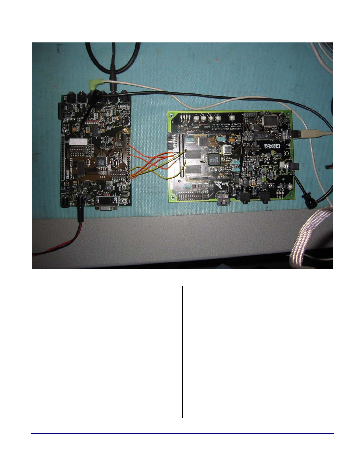
Hardware Interface
In this application, an AD73322L is connected to
SPORT1 on the ADSP-BF535 (see Figure 1).
The AD73322L is a 16-bit Codec operating from
a single supply down to 2.7V. It has a
programmable sample rate up to 64KHz. To
avoid any voltage translation when connecting it
to the ADSP-BF535, the codec should be
operated at 3.3V (same as the Blackfin® I/O
voltage). We tested the AD73322L-ADSPBF535 interface in two configurations: single
codec, dual channel and cascaded eight channel
modes. Figure 2 shows the single, dual channel
glueless connection to the ADSP-BF535. Figure
3 shows the cascaded eight channel connection
to the ADSP-BF535 (assembly code for the
eight-channel operation is not shown in this note
but is part of the VisualDSP++™ 3.1 project ZIP
file).
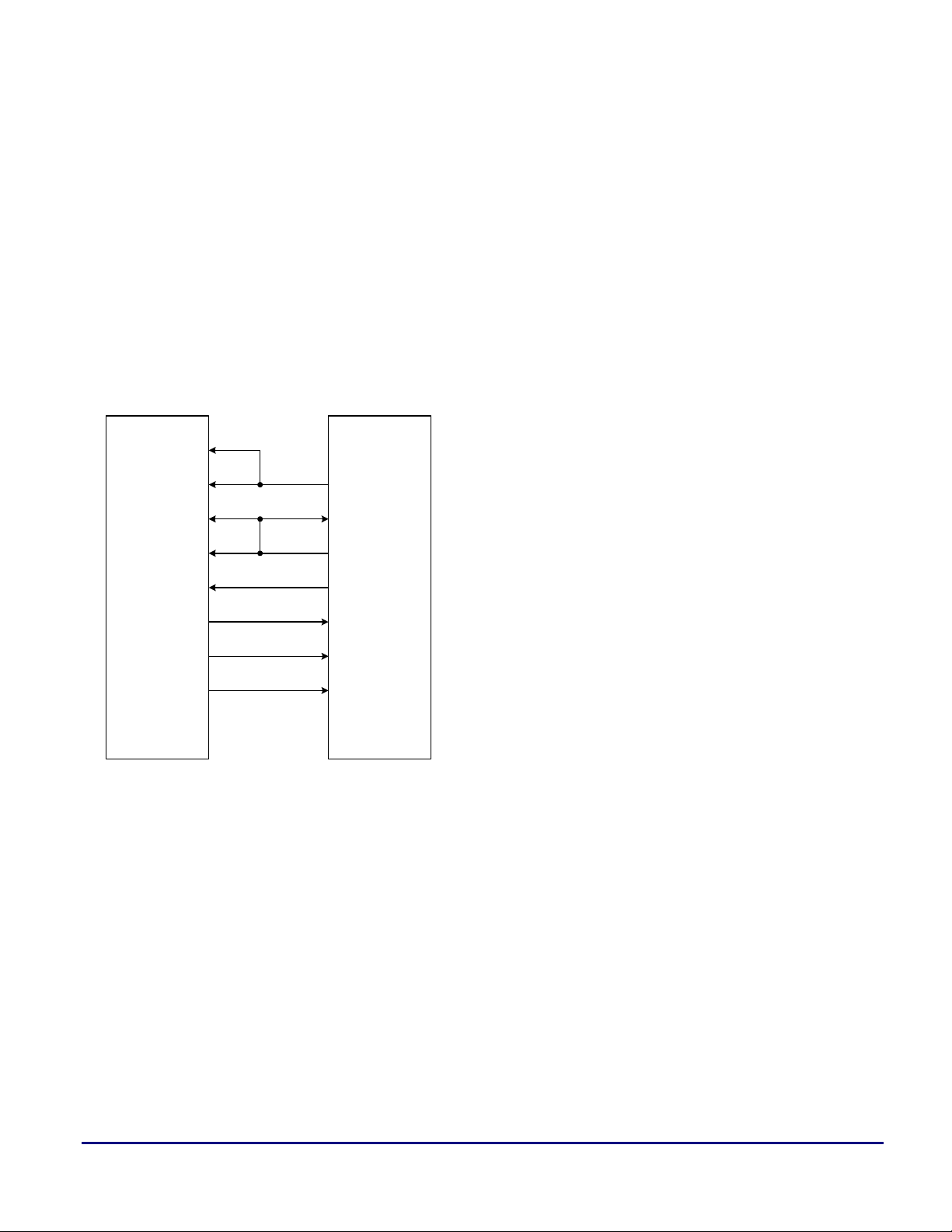
In order to synchronize the codec to the ADSPBF535 processor, we connected the AD73322L
SE (serial enable) control line to the FP11 on
ADSP-BF535. This ensures that we are always
reading the proper channel from the codec after
initialization. When SE is de-asserted, the first
channel of the last device in the cascade chain is
transmitted back to the processor. In this way,
we can always identify which channel is coming
from the codec(s).
s
Copyright 2003, Analog Devices, Inc. All rights reserved. Analog Devices assumes no responsibility for customer product design or the use or application of
customers’ products or for any infringements of patents or rights of others which may result from Analog Devices assistance. All trademarks and logos are property
of their respective holders. Information furnished by Analog Devices Applications and Development Tools Engineers is believed to be accurate and reliable, however
no responsibility is assumed by Analog Devices regarding technical accuracy and topicality of the content provided in Analog Devices’ Engineer-to-Engineer Notes.
Page 2
a
Figure 1: ADDS-21535-EZLITE to Eval-AD73322LEB Interface
The /RESET pin of the AD73322L may be
connected to the system or hardware reset for the
ADSP-BF535 or it may be controlled using a
general purpose flag from the ADSP-BF535 (as
shown in Figure 2 and Figure 3). In the event of
tying it to the system reset, it is advisable to
operate the device in mixed mode, which allows
a software reset, otherwise there is not
convenient way of resetting the device.
Digital Interface
The AD73322L is designed to easily interface to
most common processors. The SCLK, SDO,
SDOFS, SDI, and SDIFS must be connected to
the ADSP-BF535’s Serial Clock, Receiver Data,
Interfacing the ADSP-BF535 Blackfin® Processor to the AD73322L Codec (EE-193) Page 2 of 36
Receive Data Frame Sync, Transmit Data and
Transmit Data Frame Sync pins respectively (See
Figure 2). Where it is required to configure a
cascade of up to eight codecs (four AD73322L
dual codecs), it is necessary to ensure that the
timing of the SE and /RESET signals be
synchronized at each device in the cascade. A
simple D type flip flop is sufficient to sync each
signal to the MCLK (master clock), as in Figure
2. Connection of a cascade of devices to a
ADSP-BF535 is no more complicated than
connecting a single device. Instead of
connecting the SDO and SDOFS to the DSP’s Rx
port, these are now daisy-chained to the SDI and
SDIFS of the next device in the cascade. The
SDO and SDOFS of the final device in the
Page 3
cascade are connected to the DSP’s Rx port to
complete the chain. SE and /RESET on all
devices are fed from the signals that were
synchronized with the MCLK using the circuit as
described above. The SCLK from only one
device need be connected to the DSP’s SCLK
input(s) as all devices will be running at the same
SCLK frequency and phase. Note that SCLK in
this context does not refer to the system clock on
the ADSP-BF535 but to the serial clock on the
AD73322L.
a
ADSP-BF535
RCLK1
TCLK1
RFS1
TFS1
DR1
DT1
PF10
PF11
AD73322L
SCLK
SDIFS
SDOFS
SDO
SDI
RESET
SE
Figure 2: Dual Channel CODEC-DSP connection
Interfacing the ADSP-BF535 Blackfin® Processor to the AD73322L Codec (EE-193) Page 3 of 36
Page 4
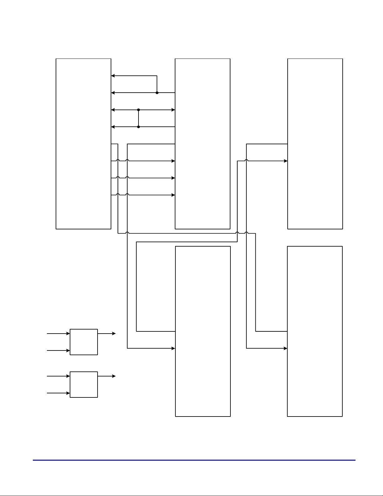
a
ADSP-BF53x AD73322L # 1
RCLK1
TCLK1
RFS1
TFS1
DR1
DT1
PF10
PF11
SCLK
SDIFS
SDOFS
SDO
SDI
RESET
SE
N/C
RFS1
TFS1
PF10
PF11
AD73322L # 3
SCLK
SDIFS
SDOFS
SDO
SDI
RESET
SE
PF11 from DSP
MCLK from Conv.
PF10 from DSP
MCLK from Conv.
D
CLK
D
CLK
74HC74
74HC74
PF11 to 73322
Q
PF10 to 73322
Q
RFS1
TFS1
PF10
AD73322L #2
SCLK
SDIFS
SDOFS
SDO
SDI
RESET
SE
N/CN/C
RFS1
TFS1
PF10
PF11PF11
AD73322L #4
SCLK
SDIFS
SDOFS
SDO
SDI
RESET
SE
Figure 3: Eight Channel CODEC-DSP Connection
Interfacing the ADSP-BF535 Blackfin® Processor to the AD73322L Codec (EE-193) Page 4 of 36
Page 5

a
ADSP-BF535 Programming Considerations
This section discusses some aspects of how the
serial port of the ADSP-BF535 should be
configured and the implications of whether Rx
and Tx interrupts should be enabled.
Following are the key settings of the ADSPBF535 SPORT required for the successful
operation with the AD73322L:
• Configure for External SPORT serial clock.
• Serial Word Length = 16 bits.
• Transmit and Receive Frame Syncs required
with every word.
• Receive Frame Sync is an input to the DSP.
• Transmit Frame Sync is an:
Input—in Frame Sync Loop-Back Mode
Output—in Nonframe Sync Loop-Back
Mode.
• Frame Syncs occur one SPORT serial clock
cycle before the MSB of the serial word.
• Frame Syncs are active high.
If SPORT interrupts are enabled, it is important
to note that the active signals on the frame sync
pins do not necessarily correspond with the
positions in time of where SPORT interrupts are
generated. On ADSP-BF535 processor, it is
necessary to enable SPORT interrupts and use
Interrupt Service Routines (ISRs) to handle
Tx/Rx activity.
ADSP-BF535 Software Considerations
Sync Loop Back (FSLB) or NonFSLB when
deciding on DSP to AFE connectivity. There is
also a choice to be made between using
autobuffering of input and output samples or
simply choosing to accept them as individual
interrupts. As most modern DSP engines support
these modes, this appendix will attempt to
discuss these topics in a generic DSP sense.
Operating Mode
The AD73322L supports two basic operating
modes: FSLB and NonFSLB. As described
previously, FSLB has some limitations when
used in Mixed Mode but is very suitable for use
with the autobuffering DMA feature that is
offered on many modern DSPs (including the
ADSP-BF535). Autobuffering allows the user to
specify the number of input or output words
(samples) that are transferred before a specific
Tx or Rx SPORT interrupt is generated. Given
that the AD73322L outputs two sample words
per sample period, it is possible using
autobuffering to have the ADSP-BF535 SPORT
generate a single interrupt on receipt of the
second of the two sample words (Appendix 1 is a
very simple autobuffer DMA example).
Additionally, both samples could be stored in a
data buffer within the data memory store. This
technique has the advantage of reducing the
number of both Tx and Rx SPORT interrupts to a
single one at each sample interval. The user also
knows where each sample is stored. The
alternative is to handle a larger number of
SPORT interrupts (twice as many in the case of a
single AD73322L) while also having some status
flags to indicate where each new sample comes
from (or is destined for).
It is important when choosing the operating
mode and hardware configuration of the
AD73322L to be aware of their implications for
ADSP-BF535 software operation. The user has
the flexibility of choosing from either Frame
Interfacing the ADSP-BF535 Blackfin® Processor to the AD73322L Codec (EE-193) Page 5 of 36
Mixed-Mode Operation
To take full advantage of mixed-mode operation,
it is necessary to configure the ADSPBF535/Codec interface in NonFSLB and to
disable autobuffering (see Appendix 2). This
Page 6
a
allows a variable numbers of words to be sent to
the AD73322L in each sample period—the extra
words being control words that are typically used
to update gain settings in adaptive control
applications. The recommended sequence for
updating control registers in mixed mode is to
send the control word(s) first before the DAC
update word. This EE note used this method and
provides two listings. Appendix 1 is the
assembly code for a single AD73322 codec. See
Figure 4 for a Logic Analyzer plot of the relevant
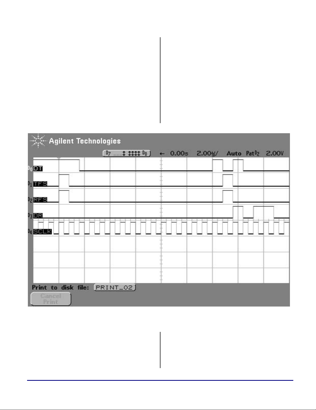
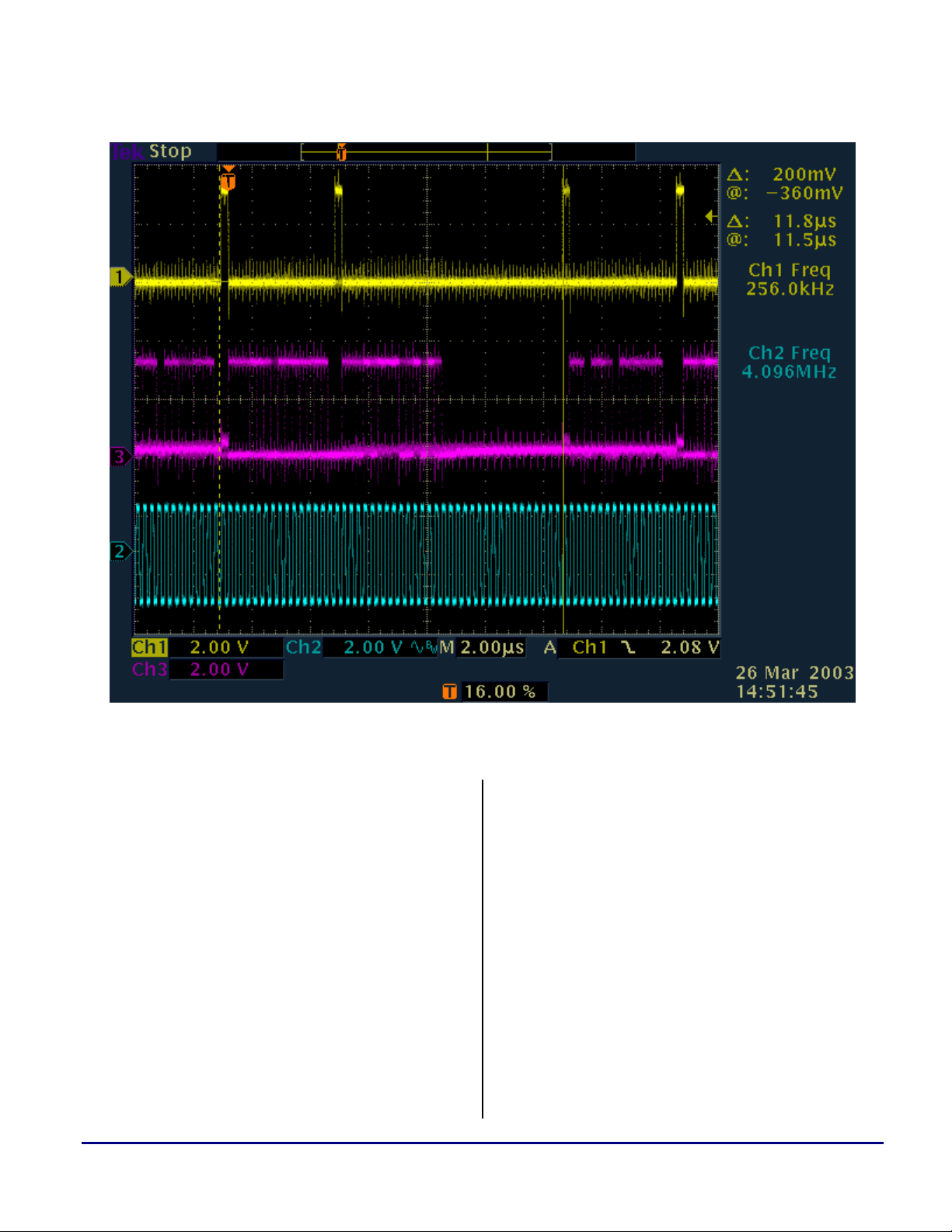
timing signals. Also, See Figure 5 for a scope
plot of necessary timing (blue=clock,
yellow=frame and purple=data). You can see
from these two figures that each 16-bit word has
a 1-bit frame signal that proceeds the data by one
SCLK. Due to this functionality, Multi-channel
Mode (MCM or TDM) SPORT modes do not
work with this codec. As a result, we are forced
to use either autobuffer DMA or interrupts to
process each and every 16-bit word.
Figure 4: Logic Analyzer of AD73322L Timing
It is possible to use mixed-mode operation when
configured in FSLB, but it is necessary to replace
the DAC update with a control word write in
each sample period which may cause some
discontinuity in the output signal due to a sample
Interfacing the ADSP-BF535 Blackfin® Processor to the AD73322L Codec (EE-193) Page 6 of 36
point being missed and the previous sample
being repeated. This however may be acceptable
in some cases as the effect may be masked by
gain changes, etc.
Page 7
a
Figure 5: Scope plot of two channels
Interrupts
The AD73322L transfers and receives
information over the serial connection from the
ADSP-BF535 SPORT. This occurs following
reset during the initialization phase—and in both
data-mode and mixed-mode. Each transfer of
data to or from the ADSP-BF535 can cause a
SPORT interrupt to occur. However even in
FSLB configuration where serial transfers in and
out of the DSP are synchronous, it is important to
note that Tx and Rx interrupts do not occur at the
same time due to the way that Tx and Rx
interrupts are generated internally within the
ADSP-BF535’s SPORT. This is especially
important in time critical control loop
Interfacing the ADSP-BF535 Blackfin® Processor to the AD73322L Codec (EE-193) Page 7 of 36
applications where it may be necessary to use Rx
interrupts only, as the relative positioning of the
Tx interrupts relative to the Rx interrupts in a
single sample interval are not suitable for quick
update of new DAC positions.
AD73322L Initialization
Following reset, the AD73322L is in its default
condition which ensures that the device is in
Control Mode and must be programmed or
initialized from the ADSP-BF535 to start
conversions. As communications between
AD73322L and the ADSP-BF535 are interrupt
driven, it is usually not practical to embed the
Page 8

a
initialization codes into the body of the
Conclusions
initialization routine. It is more practical to put
the sequence of initialization codes in a memory
buffer and to access this buffer with a pointer
that is updated on each interrupt. If a circular
buffer is used, it allows the interrupt routine to
check when the circular buffer pointer has
wrapped around—at which point the
initialization sequence is complete. In FSLB
configurations, a single control word per codec
per sample period is sent to the AD73322L
whereas in NonFSLB, it is possible to initialize
the device in a single sample period provided the
SCLK rate is programmed to a high rate. It is
also possible to use autobuffering in which case
an interrupt is generated when the entire
initialization sequence has been sent to the
This note provides the hardware interface and
assembly code for ADSP-BF535 interface to
AD73322L operating in mixed mode. While this
code example is not the most efficient in terms of
the number interrupts, it does provide the most
flexibility allowing multiple AD73322L’s to be
cascaded with full control and realtime parameter
updates. Each codec will add two additional
interrupts that must be processed. The assembly
code in this example is not fully optimized and is
not C callable. Additional work should be done
to expand the simple FSLB mode (in Appendix
1) to provide a full talkthrough utilizing Tx and
Rx autobuffer DMAs.
AD73322L.
References
[1] ADSP-BF535 Blackfin® DSP Hardware Reference. Revision 1.0, Nov. 2002, Analog Devices, Inc.
[2] AD73322L, Low Cost, Low Power CMOS General Purpose Dual Analog Front End Datasheet,
Rev 0.
[3] Eval-AD73322LEB Rev 0 evaluation board.
[4] ADDS-21535-EZLITE Rev 1.5, 2001.
[5] Blackfin® VisualDSP++™ 3.1.
Appendix 1: Simple Autobuffer DMA example
73322 Test Code.asm
/* ---------------------------------------------------------------------------- */
/* 73322 Test Code */
/* */
/* PF10 - Reset */
/* PF11 - SE */
/* */
/* 2 CODECs wired in cascade */
/* ---------------------------------------------------------------------------- */
#include <def21535.h>
#include <SportBits.h>
/* ---------------------------------------------------------------------------- */
/* Global and External Declarations */
Interfacing the ADSP-BF535 Blackfin® Processor to the AD73322L Codec (EE-193) Page 8 of 36
Page 9

a
.GLOBAL Start;
.EXTERN _EHANDLER;
.EXTERN _RHANDLER;
.EXTERN _NHANDLER;
.EXTERN _XHANDLER;
.EXTERN _HWHANDLER;
.EXTERN _THANDLER;
.EXTERN _RTCHANDLER;
.EXTERN _SportISR;
.EXTERN _I9HANDLER;
.EXTERN _I10HANDLER;
.EXTERN _I11HANDLER;
.EXTERN _I12HANDLER;
.EXTERN _I13HANDLER;
.EXTERN _I14HANDLER;
.EXTERN _I15HANDLER;
/* ---------------------------------------------------------------------------- */
/* Data Memory */
.SECTION Buffers;
.byte2 TxBuf[18] = // for 1 device
/*5432109876543210*/
b#1000100100000110, // CRB - DmClk=MCLK=10MHz, SCLK=MCLK,
// Fs= DMCLK/256=39.0625KHz
b#1000000100000110, // CRB - DmClk=MCLK=10MHz, SCLK=MCLK,
// Fs= DMCLK/256=39.0625KHz
b#1000101000111101, // CRC - RefOut=Disabled, Ref Power=On,
// InAmp=Off, Gain Tap=Off
b#1000001000111101, // CRC - RefOut=Disabled, Ref Power=On,
// InAmp=Off, Gain Tap=Off
b#1000101100000000, // CRD - I/O gain=0, ADC Mod=Off, Mute=Off
b#1000001100000000, // CRD - I/O gain=0, ADC Mod=Off, Mute=Off
b#1000110000000000, // CRE - Dac=0, DGain tap=Disabled,
// InterpolatorBypass=Disabled
b#1000010000000000, // CRE - Dac=0, DGain tap=Disabled,
// InterpolatorBypass=Disabled
b#1000110100000000, // CRF - A Gain Tap=0, Single Ended,
// A Gain Tap=Disables,
b#1000010000000000, // CRF - Dac=0, DGain tap=Disabled
// InterpolatorBypass=Disabled
b#1000111000000000, // CRG - Digital Gain Tap Coef0-7=0
b#1000011000000000, // CRG - Digital Gain Tap Coef0-7=0
b#1000111100000000, // CRH - Digital Gain Tap Coef8-15=0
b#1000011100000000, // CRH - Digital Gain Tap Coef8-15=0
/* 5432109876543210 */
b#1000100000010000, // CRA - Program Mode, Mixed Mode=Off,
// Dig/SPORT LoopBack=0, Device Count=1
Interfacing the ADSP-BF535 Blackfin® Processor to the AD73322L Codec (EE-193) Page 9 of 36
Page 10

a
b#1000000000010000, // CRA - Program Mode, Mixed Mode=Off,
// Dog/SPORT LoopBack=0, Device Count=1
b#1000100000010001, // CRA - Data Mode, Mixed Mode=Off, LoopBack=0,
// Device Count=1
b#1000000000010001; // CRA - Data Mode, Mixed Mode=Off, LoopBack=0,
// Device Count=1
.byte2 TxBuf4[32] = // for 2 devices
/*5432109876543210*/
b#1001100100001111, // CRB - DmClk=MCLK=10MHz, SCLK=MCLK,
// Fs= DMCLK/256=39.0625KHz
b#1001000100001111, // CRB - DmClk=MCLK=10MHz, SCLK=MCLK,
// Fs= DMCLK/256=39.0625KHz
b#1000100100001111, // CRB - DmClk=MCLK=10MHz, SCLK=MCLK,
// Fs= DMCLK/256=39.0625KHz
b#1000000100001111, // CRB - DmClk=MCLK=10MHz, SCLK=MCLK,
// Fs= DMCLK/256=39.0625KHz
b#1001101000100001, // CRC - RefOut=Disabled, Ref Power=On,
// InAmp=Off, Gain Tap=Off
b#1001001000100001, // CRC - ditto
b#1000101000100001, // CRC - RefOut=Disabled, Ref Power=On,
// InAmp=Off, Gain Tap=Off
b#1000001000100001, // CRC - ditto
b#1001101100000000, // CRD - I/O gain=0, ADC Mod=Off, Mute=Off
b#1001001100000000, // CRD - ditto
b#1000101100000000, // CRD - I/O gain=0, ADC Mod=Off, Mute=Off
b#1000001100000000, // CRD - ditto
b#1001110000000000, // CRE - Dac=0, InterpolatorBypass=Disabled,
// DGain tap=Disabled
b#1001010000000000, // CRE - ditto
b#1000110000000000, // CRE - Dac=0, InterpolatorBypass=Disabled,
// DGain tap=Disabled
b#1000010000000000, // CRE - ditto
b#1001110100000000, // CRF - A Gain Tap=0, Single Ended,
// A Gain Tap=Disables,
b#1001010100000000, // CRF - Input not inverted, LoopBack=Disabled,
// A Gain Tap Muted
b#1000110100000000, // CRF - A Gain Tap=0, Single Ended,
// A Gain Tap=Disables,
b#1000010100000000, // CRF - Input not inverted, LoopBack=Disabled,
// A Gain Tap Muted
b#1001111000000000, // CRG - Digital Gain Tap Coef0-7=0
b#1001011000000000, // CRG - ditto
b#1000111000000000, // CRG - Digital Gain Tap Coef0-7=0
b#1000011000000000, // CRG - ditto
b#1001111100000000, // CRH - Digital Gain Tap Coef8-15=0
b#1001011100000000, // CRH - ditto
b#1000111100000000, // CRH - Digital Gain Tap Coef8-15=0
b#1000011100000000, // CRH - ditto
b#1001100000110001, // CRA - Data Mode, Mixed Mode=Off, LoopBack=0,
Interfacing the ADSP-BF535 Blackfin® Processor to the AD73322L Codec (EE-193) Page 10 of 36
Page 11

a
// Device Count=1
b#1001000000110001, // CRA - Reset=Off
b#1000100000110001, // CRA - Data Mode, Mixed Mode=Off, LoopBack=0,
// Device Count=1
b#1000000000110001; // CRA - Reset=Off
#define RxBufLen 12000
.var RxBuf[RxBufLen];
/* ---------------------------------------------------------------------------- */
// Code Start.....
.Section ProgramCode;
// Note: should add in check for SIC_IMASK in Rev 0.2 and 1.0 silicon of the ADSP// BF535 (should be inverted polarity).
// Setup Event Vectors and Handlers
SETUP: R0 = 0;
LoadP0(EVT0)
r1 = _EHANDLER (Z);
r1.h = _EHANDLER; // Emulation Handler (Int0)
[ P0 ++ ] = R1;
R0 = _RHANDLER (Z);
R0.H = _RHANDLER; // Reset Handler (Int1)
[ P0 ++ ] = R0;
R0 = _NHANDLER (Z);
R0.H = _NHANDLER; // NMI Handler (Int2)
[ P0 ++ ] = R0;
R0.L = _XHANDLER;
R0.H = _XHANDLER; // Exception Handler (Int3)
[ P0 ++ ] = R0;
[ P0 ++ ] = R0; // IVT4 isn't used
R0 = _HWHANDLER (Z);
R0.H = _HWHANDLER; // HW Error Handler (Int5)
[ P0 ++ ] = R0;
R0 = _THANDLER (Z);
R0.H = _THANDLER; // Timer Handler (Int6)
[ P0 ++ ] = R0;
R0 = _RTCHANDLER (Z);
R0.H = _RTCHANDLER; // IVG7 Handler
[ P0 ++ ] = R0;
R0 = _SportISR (Z);
R0.H = _SportISR; // IVG8 Handler
[ P0 ++ ] = R0;
R0 = _I9HANDLER (Z);
R0.H = _I9HANDLER; // IVG9 Handler
[ P0 ++ ] = R0;
Interfacing the ADSP-BF535 Blackfin® Processor to the AD73322L Codec (EE-193) Page 11 of 36
Page 12

a
R0 = _I10HANDLER (Z);
R0.H = _I10HANDLER; // IVG10 Handler
[ P0 ++ ] = R0;
R0 = _I11HANDLER (Z);
R0.H = _I11HANDLER; // IVG11 Handler
[ P0 ++ ] = R0;
R0 = _I12HANDLER (Z);
R0.H = _I12HANDLER; // IVG12 Handler
[ P0 ++ ] = R0;
R0 = _I13HANDLER (Z);
R0.H = _I13HANDLER; // IVG13 Handler
[ P0 ++ ] = R0;
R0 = _I14HANDLER (Z);
R0.H = _I14HANDLER; // IVG14 Handler
[ P0 ++ ] = R0;
R0 = _I15HANDLER (Z);
R0.H = _I15HANDLER; // IVG15 Handler
[ P0 ++ ] = R0;
// P0.L = EVT_OVERRIDE & 0xffff; // added in to address anomaly 20 for rev
// 0.1 ADSP-21535 silicon
// P0.H = EVT_OVERRIDE >> 16;
// R0 = 0;
// [ P0 ] = R0; ssync;
SP.H = 0xF003; // Set up supervisor stack
SP.L = 0xFFDC;
LoadP0(EVT15) // Point to IVG15 in Event Vector Table
P1.L = Start; //Point to start of code
P1.H = Start;
[P0] = P1; ssync; // Place the address of start code in
// IVG15 of EVT
P0.L = IMASK & 0xFFFF;
R0 = W[P0];
bitset(r0,15); // Set(enable) IVG15 bit in Interrupt
// Mask Register
W[P0] = R0; ssync;
RAISE 15; // Invoke IVG15 interrupt
P0.l = WAIT_HERE;
P0.h = WAIT_HERE;
RETI = P0;
nop;
nop;
nop;
nop;
RTI; // Return from Reset Interrupt
WAIT_HERE: // Wait here till IVG15 interrupt is
Interfacing the ADSP-BF535 Blackfin® Processor to the AD73322L Codec (EE-193) Page 12 of 36
Page 13

a
// processed
JUMP WAIT_HERE;
// ----------------------------------------------------------------------------
// Main code starts here .....
Start: [--SP] = RETI; // RETI must be pushed to enable
// interrupts. Boot code in supervisor
// mode starts here.
call GeneralPurposeInit;
call Sport1Inits;
call SportIRQInits;
call Sport1TxDMASetup;
call Program73322s;
// call Sport1TxDMASetup2; // Added (JWS)
call Sport1RxDMASetup;
call Recieve73322Data;
DieHere:
nop;
nop;
nop;
nop;
jump DieHere;
// ----------------------------------------------------------------------------
// Subs Start.....
// init PFs and blink LEDs, reset CODEC
GeneralPurposeInit:
// initalize pointer registers and data registers
R0 = 0; R1 = 0; R2 = 0; R3 = 0; R4 = 0; R5 = 0; R6 = 0; R7 = 0;
P0 = 0; P1 = 0; P2 = 0; P3 = 0; P4 = 0; P5 = 0;
// initialize the DAG registers
I0 = 0 (X); I1 = 0 (X); I2 = 0 (X); I3 = 0 (X);
M0 = 0 (X); M1 = 0 (X); M2 = 0 (X); M3 = 0 (X);
L0 = 0 (X); L1 = 0 (X); L2 = 0 (X); L3 = 0 (X);
B0 = 0 (X); B1 = 0 (X); B2 = 0 (X); B3 = 0 (X);
LoadP0(FIO_DIR) // config PF I/O bits as outputs
R0.l = w[P0];
bitset (R0, Reset);
bitset (R0, SE);
bitset (R0, LED);
w[P0] = R0.l; ssync;
LoadP0(FIO_FLAG_S) // Set Init state for SE, Reset and LED == ON
R0.l = 0x0C01;
w[P0] = R0.l; ssync;
P5.l = 0x0000;
p5.h = 0x1000;
loop blink_LEDs lc0=P5;
Interfacing the ADSP-BF535 Blackfin® Processor to the AD73322L Codec (EE-193) Page 13 of 36
Page 14

a
loop_begin blink_LEDs;
nop;
loop_end blink_LEDs;
LoadP0(FIO_FLAG_C) // reset 73322, turn off LED
r0.l = 0x0C01;
w[P0] = R0.l; ssync;
P5 = 0x00000140; // hold reset for about 1uS
loop hold_Reset lc0=P5;
loop_begin hold_Reset;
nop;
loop_end hold_Reset;
LoadP0(FIO_FLAG_S) // release the Reset line, turn on LED
r0.l = 0x0401;
w[P0] = R0.l; ssync;
p5.l = 0xd480; // allow CODEC time to recouver from Reset
P5.h = 0x3F00;
loop ResetRecouver lc0=P5;
loop_begin ResetRecouver;
nop;
loop_end ResetRecouver;
rts;
// ----------------------------------------------------------------------------
Sport1Inits:
R0 = 0x0000;
LoadP0(SPORT1_TX_CONFIG)
w[P0] = R0; ssync;
LoadP0(SPORT1_RX_CONFIG)
w[P0] = R0; ssync;
LoadP0(SPORT1_CONFIG_DMA_TX)
w[P0] = R0; ssync;
LoadP0(SPORT1_CONFIG_DMA_RX)
w[P0] = R0; ssync;
LoadP0(SPORT1_MCMC1)
w[P0] = R0; ssync;
LoadP0(SPORT1_MCMC2)
w[P0] = R0; ssync;
LoadP0(SPORT1_IRQSTAT_RX) // this clears any Rx errors
R0.l = 0x07;
w[P0] = R0; ssync;
LoadP0(SPORT1_IRQSTAT_TX) // this clears any Tx errors
R0.l = 0x07;
w[P0] = R0; ssync;
R0.l = (TFSR + BITS16);
LoadP0(SPORT1_TX_CONFIG)
w[P0] = R0; ssync;
Interfacing the ADSP-BF535 Blackfin® Processor to the AD73322L Codec (EE-193) Page 14 of 36
Page 15

a
R0.l = (RFSR + BITS16);
LoadP0(SPORT1_RX_CONFIG)
w[P0] = R0; ssync;
rts;
// ----------------------------------------------------------------------------
SportIRQInits:
R0.h = 0xFFFF; // enables Sport1 IRQs, old =0x000000C0, Errata #8
R0.l = 0xFF3F;
LoadP0(SIC_IMASK)
w[P0] = R0; ssync;
R0.l = 0x011F; // enables IVG8
LoadP0(IMASK)
w[P0] = R0; ssync;
rts;
// ----------------------------------------------------------------------------
Program73322s:
LoadP0(FIO_FLAG_C) // clear SE (disable the CODEC)
R0.l = 0;
bitset (R0, SE);
w[P0] = R0.l; ssync;
R0.l = 0x0015; // autobuffer, int on complete, DMA enabled
LoadP0(SPORT1_CONFIG_DMA_TX)
w[p0] = R0; ssync;
LoadP0(SPORT1_TX_CONFIG)
R0 = w[p0];
Bitset(R0, TSPEN); // enable Sport1
w[p0] = R0; ssync;
R7 = 0x0000; // TX IRQ flag
LoadP0 (FIO_FLAG_S) // enable the CODEC: SE = 1
R0 = w[P0];
bitset (R0, SE);
w[P0] = R0; ssync;
WaitOnTx: // interrupt should be generated here !?!?!
nop;
nop;
nop;
nop;
rts;
// ----------------------------------------------------------------------------
Recieve73322Data:
LoadP0(FIO_FLAG_C) // clear SE (disable the CODEC)
R0.l = 0;
bitset (R0, SE);
w[P0] = R0.l; ssync;
Interfacing the ADSP-BF535 Blackfin® Processor to the AD73322L Codec (EE-193) Page 15 of 36
Page 16

a
R0.l = 0x0017; // autobuffer, int on complete, DMA enabled
LoadP0(SPORT1_CONFIG_DMA_RX)
w[p0] = R0.l; ssync;
/* R0.l = 0x0015; // (JWS) autobuffer, int on complete, DMA enabled
LoadP0(SPORT1_CONFIG_DMA_TX)
w[p0] = R0; ssync;
LoadP0(SPORT1_TX_CONFIG)
R0 = w[p0];
Bitset(R0, TSPEN); // enable Sport1
w[p0] = R0; ssync;
R7 = 0x0000; // TX IRQ flag
*/
LoadP0(SPORT1_RX_CONFIG)
R0.l = w[p0];
Bitset(R0, RSPEN); // enable Sport1
w[p0] = R0.l; ssync;
LoadP0(FIO_FLAG_S) // enable CODEC: SE = 1
R0.l = w[P0];
bitset (R0, SE);
w[P0] = R0; ssync;
WaitOnRx:
nop; // interrupt should be generated here !?!?!
nop;
nop;
nop;
rts;
// ----------------------------------------------------------------------------
Sport1TxDMASetup:
R0.l = 0x0014; // enable autobuffer
// DCOME set to 1 (interrupt on completion)
LoadP0(SPORT1_CONFIG_DMA_TX)
w[p0] = R0; ssync;
R0.l = (TxBuf >> 16) & 0xFFFF; // load start address HI word
LoadP0(SPORT1_START_ADDR_HI_TX)
w[p0] = R0; ssync;
R0.l = TxBuf & 0xFFFF; // load start address Lo word
LoadP0(SPORT1_START_ADDR_LO_TX)
w[p0] = R0; ssync;
R0.l = LENGTH (TxBuf); // load length of buffer
LoadP0(SPORT1_COUNT_TX)
w[p0] = R0; ssync;
rts;
// ----------------------------------------------------------------------------
Sport1RxDMASetup:
Interfacing the ADSP-BF535 Blackfin® Processor to the AD73322L Codec (EE-193) Page 16 of 36
Page 17

a
R0.l = 0x0014; // DCOME set to 1
LoadP0(SPORT1_CONFIG_DMA_RX)
w[p0] = R0; ssync;
R0.l = (RxBuf >> 16) & 0xFFFF;
LoadP0(SPORT1_START_ADDR_HI_RX)
w[p0] = R0; ssync;
R0.l = RxBuf & 0xFFFF;
LoadP0(SPORT1_START_ADDR_LO_RX)
w[p0] = R0; ssync;
R0.l = LENGTH (RxBuf);
LoadP0(SPORT1_COUNT_RX)
w[p0] = R0; ssync;
rts;
// ------------------------------------------------------------------------
Listing 1: 73322 Test Code.asm
73322 IRQ Test Code.asm
// ---------------------------------------------------------------------------//
// 73322 Test Code
//
// Interrupt Service Routines
//
// Nov 7 / 02
//
// ----------------------------------------------------------------------------
#include <def21535.h>
#include <SportBits.h>
// ---------------------------------------------------------------------------// Global and External Declarations
.global _EHANDLER;
.global _RHANDLER;
.global _NHANDLER;
.global _XHANDLER;
.global _HWHANDLER;
.global _THANDLER;
.global _RTCHANDLER;
.global _SportISR;
.global _I9HANDLER;
.global _I10HANDLER;
.global _I11HANDLER;
.global _I12HANDLER;
.global _I13HANDLER;
.global _I14HANDLER;
.global _I15HANDLER;
// ---------------------------------------------------------------------------// Sport1 TX ISR
Interfacing the ADSP-BF535 Blackfin® Processor to the AD73322L Codec (EE-193) Page 17 of 36
Page 18

a
.Section ISRCode;
_SportISR:
[--SP] = (r7:0);
[--SP] = (p5:0);
LoadP0(SIC_ISR) // read MMR to determine what caused the interrupt
R0 = [P0];
cc = bittst (R0, 4);
if cc jump SportRxISR;
// ---------------------------------------------------------------------------// Sport1 Tx ISR
SportTxISR:
cc = bittst (R7, 0); // test flag
if !CC jump int5_done; // if set
bitset (R7,0);
(p5:0) = [SP++]; // Restore Regs
(r7:0) = [SP++];
rti;
int5_done:
LoadP0(SIC_IMASK)
R0 = w[P0];
bitset (R0,7); // Use to be "bitclr"..Errata #8, SIC_IMASK inversion
w[P0] = R0; ssync;
R7 = 0;
(p5:0) = [SP++]; // Restore Regs
(r7:0) = [SP++];
rti;
// ---------------------------------------------------------------------------// Sport1 Rx ISR
SportRxISR:
// R0 = 0x0C0; // old=0x0C0, Errata #8
R0.h = 0xFFFF; // enables Sport1 IRQs, old =0x000000C0, Errata #8
R0.l = 0xFF3F;
LoadP0(SIC_IMASK)
w[P0] = R0; ssync;
(p5:0) = [SP++]; // Restore Regs
(r7:0) = [SP++];
rti;
_EHANDLER: // Emulation Handler 0
RTE;
_RHANDLER: // Reset Handler 1
RTI;
_NHANDLER: // NMI Handler 2
RTN;
_XHANDLER: // Exception Handler 3
RTX;
Interfacing the ADSP-BF535 Blackfin® Processor to the AD73322L Codec (EE-193) Page 18 of 36
Page 19

_HWHANDLER: // HW Error Handler 5
RTI;
_THANDLER: // Timer Handler 6
RTI;
_RTCHANDLER: // IVG 7 Handler (RTC)
RTI;
_I9HANDLER: // IVG 9 Handler
RTI;
_I10HANDLER: // IVG 10 Handler
RTI;
_I11HANDLER: // IVG 11 Handler
RTI;
_I12HANDLER: // IVG 12 Handler
RTI;
_I13HANDLER: // IVG 13 Handler
RTI;
_I14HANDLER:
RTI;
_I15HANDLER:
nop;
nop;
nop;
nop;
RTI;
a
Listing 2: 73322 IRQ Test Code.asm
Appendix 2: Interrupt driven Non-DMA 2-Channel assembly code
Defines.asm
/* Tx Config Register bits */
#define ZERO_FILL 0
#define SIGN_EXT 4
#define MU_LAW 8
#define A_LAW 0xC
#define LSB_FIRST 0x10
#define BITS16 0x1E0
#define BITS8 0x0E0
#define ITFS 0x200 /* internal xmit frame sync */
#define TFSR 0x400 /* xmit frame sync required */
#define DITFS 0x800
#define LTFS 0x1000 /* active low frame sync */
#define LATFS 0x2000 /* late frame sync */
#define CKRE 0x4000 /* sample data on rising edge of bitclk */
#define ICLKD 0x8000 // Internal Clock Disable
Interfacing the ADSP-BF535 Blackfin® Processor to the AD73322L Codec (EE-193) Page 19 of 36
Page 20

a
/* Rx Config Register bits */
#define RSPEN 0 /* rx enable */
#define IRFS 0x200 /* use internal frame sync */
#define RFSR 0x400 /* rx frame sync required */
#define LRFS 0x1000 /* active lo rx frame sync */
#define LARFS 0x2000 /* late rx frame sync */
/* SPORT Register Bits */
#define RXS 1 /* Status register: Receive Status bit */
#define TXS 2 /* Status register: Transmit Status bit */
#define TSPEN 0 /* TX Config reg: Tx Sport Enable */
#define CODEC_INIT_Length 18
#define RxBufLength 256
#define TxBufLength 256
#define SineCosTableLength 32
#define NoChannels 2
/* ---------------------------------------------------------------------------- */
// Macros Here.....
#define SE 0x0B
#define Reset 0x0A
#define LED 0x00
#define Loadd(a,b)\
a.l=b & 0xFFFF;\
a.h=(b >> 16) & 0xFFFF;
#define Load(c,b)\
a.l=b;\
a.h=b;
#define LoaddP0(a)\
P0.l=a & 0xFFFF;\
P0.h=(a >> 16) & 0xFFFF;
#define LoadP0(a)\
P0.l=a;\
P0.h=a;
#define LoaddP1(a)\
P1.l=a & 0xFFFF;\
P1.h=(a >> 16) & 0xFFFF;
#define LoadP1(a)\
P1.l=a;\
P1.h=a;
#define LoaddP2(a)\
P2.l=a & 0xFFFF;\
P2.h=(a >> 16) & 0xFFFF;
#define LoadP2(a)\
P2.l=a;\
Interfacing the ADSP-BF535 Blackfin® Processor to the AD73322L Codec (EE-193) Page 20 of 36
Page 21

P2.h=a;
#define LoaddP3(a)\
P3.l=a & 0xFFFF;\
P3.h=(a >> 16) & 0xFFFF;
#define LoadP3(a)\
P3.l=a;\
P3.h=a;
#define LoaddP4(a)\
P4.l=a & 0xFFFF;\
P4.h=(a >> 16) & 0xFFFF;
#define LoadP4(a)\
P4.l=a;\
P4.h=a;
#define LoaddP5(a)\
P5.l=a & 0xFFFF;\
P5.h=(a >> 16) & 0xFFFF;
#define LoadP5(a)\
P5.l=a;\
P5.h=a;
#define LoaddR0(a)\
R0.l=a & 0xFFFF;\
R0.h=(a >> 16) & 0xFFFF;
#define LoadR0(a)\
R0.l=a;\
R0.h=a;
#define LoaddR5(a)\
R5.l=a & 0xFFFF;\
R5.h=(a >> 16) & 0xFFFF;
#define LoadR5(a)\
R5.l=a;\
R5.h=a;
#define LoaddR6(a)\
R6.l=a & 0xFFFF;\
R6.h=(a >> 16) & 0xFFFF;
#define LoadR6(a)\
R6.l=a;\
R6.h=a;
a
Listing 3: Defines.h
FinalTestBuffers.asm
// ---------------------------------------------------------------------------// Buffers and CODEC initialization codes
// ----------------------------------------------------------------------------
Interfacing the ADSP-BF535 Blackfin® Processor to the AD73322L Codec (EE-193) Page 21 of 36
Page 22

a
#include <defines.h>
// ---------------------------------------------------------------------------// Global and External definitions
.global Done;
.global Channel;
.global CODEC_Init_Data;
.global SineCos1;
.global SineCos2;
.global SineCos3;
.global SineCos4;
.global SineCos5;
.global SineCos6;
.global SineCos7;
.global SineCos8;
.global RxBufPointer;
.global RxBuf1;
.global RxBuf2;
.global RxBuf3;
.global RxBuf4;
.global RxBuf5;
.global RxBuf6;
.global RxBuf7;
.global RxBuf8;
.global RxChannelEnables;
.global TxBufPointer;
.global TxBuf1;
.global TxBuf2;
.global TxBuf3;
.global TxBuf4;
.global TxBuf5;
.global TxBuf6;
.global TxBuf7;
.global TxBuf8;
.global TxChannelEnables;
// ---------------------------------------------------------------------------// Data Memory
.Section Buffers;
// ---------------------------------------------------------------------------// misc variables
.byte2 Done;
.byte2 Channel;
.byte RxChannelEnables[8];
.byte TxChannelEnables[8];
// ---------------------------------------------------------------------------// Actual Tx and Rx buffers and pointers
.byte2 RxBufPointer;
.byte2 RxBuf1[RxBufLength];
.byte2 RxBuf2[RxBufLength];
Interfacing the ADSP-BF535 Blackfin® Processor to the AD73322L Codec (EE-193) Page 22 of 36
Page 23

a
.byte2 RxBuf3[RxBufLength];
.byte2 RxBuf4[RxBufLength];
.byte2 RxBuf5[RxBufLength];
.byte2 RxBuf6[RxBufLength];
.byte2 RxBuf7[RxBufLength];
.byte2 RxBuf8[RxBufLength];
.byte2 TxBufPointer;
.byte2 TxBuf1[TxBufLength];
.byte2 TxBuf2[TxBufLength];
.byte2 TxBuf3[TxBufLength];
.byte2 TxBuf4[TxBufLength];
.byte2 TxBuf5[TxBufLength];
.byte2 TxBuf6[TxBufLength];
.byte2 TxBuf7[TxBufLength];
.byte2 TxBuf8[TxBufLength];
// ---------------------------------------------------------------------------// CODEC initialization strings.
// to be copied into TxBuf1
.byte2 CODEC_Init_Data[CODEC_INIT_Length] =
// 5432109876543210
b#1000100100000111, // CRB - DMCLK/256=64KHz=Fs,
// SCLK=DMCLK/4=4.096MHz, DMCLK=MCLK
b#1000000100000111, // CRB - DMCLK/256=64KHz=Fs,
// SCLK=DMCLK/4=4.096MHz, DMCLK=MCLK
// 5432109876543210
b#1000101000111101, // CRC - RefOut=Disabled, Ref Power=On,
// InAmp=Off, Gain Tap=Off
b#1000001000111101, // CRC - RefOut=Disabled, Ref Power=On,
// InAmp=Off, Gain Tap=Off
// 5432109876543210
b#1000101100000000, // CRD - I/O gain=0, ADC Mod=Off, Mute=Off
b#1000001100000000, // CRD - I/O gain=0, ADC Mod=Off, Mute=Off
// 5432109876543210
b#1000110000000000, // CRE - Dac=0, DGain tap=Disabled,
// InterpolatorBypass=Disabled
b#1000010000000000, // CRE - Dac=0, DGain tap=Disabled,
// InterpolatorBypass=Disabled
// 5432109876543210
b#1000110100000000, // CRF - A Gain Tap=0, Single Ended,
// A Gain Tap=Disables,
b#1000010000000000, // CRF - Dac=0, DGain tap=Disabled
// InterpolatorBypass=Disabled
// 5432109876543210
b#1000111000000000, // CRG - Digital Gain Tap Coef0-7=0
b#1000011000000000, // CRG - Digital Gain Tap Coef0-7=0
// 5432109876543210
b#1000111100000000, // CRH - Digital Gain Tap Coef8-15=0
b#1000011100000000, // CRH - Digital Gain Tap Coef8-15=0
// 5432109876543210
Interfacing the ADSP-BF535 Blackfin® Processor to the AD73322L Codec (EE-193) Page 23 of 36
Page 24

a
b#1000100000010000, // CRA - Program Mode, Mixed Mode=Off,
// Dig/SPORT LoopBack=0, Device Count=1
b#1000000000010000, // CRA - Program Mode, Mixed Mode=Off,
// Dog/SPORT LoopBack=0, Device Count=1
// 5432109876543210
b#1000100000010001, // CRA - Data Mode, Mixed Mode=Off,
// LoopBack=0, Device Count=1
b#1000000000010001; // CRA - Data Mode, Mixed Mode=Off,
// LoopBack=0, Device Count=1
// ---------------------------------------------------------------------------// Data to output to the CODECs ... Sine, Cos and 1, 2, 3 and 4 pulse trains
/* .byte2 SineCos1 [SineCosTableLength] =
0x8000,
0x8000,
.
Listing 4: FinalTestBuffers.asm
FinalTestISR.asm
// ---------------------------------------------------------------------------//
// Blackfin - 73322 Final test code
//
// Interrupt Service Routines
//
// Jan 13 / 03
//
// ----------------------------------------------------------------------------
#include <def21535.h>
#include <defines.h>
// ---------------------------------------------------------------------------// Global and External definitions
.global _EHandler;
.global _RHandler;
.global _NHandler;
.global _XHandler;
.global _HWHandler;
.global _THandler;
.global _RTCHandler;
.global _Sport1ISR;
.global _CODEC_INIT_ISR;
.global _I9Handler;
.global _I10Handler;
.global _I11Handler;
.global _I12Handler;
.global _I13Handler;
.global _I14Handler;
.global _I15Handler;
.extern RxBufPointer;
.extern RxChannelEnables;
Interfacing the ADSP-BF535 Blackfin® Processor to the AD73322L Codec (EE-193) Page 24 of 36
Page 25

a
.extern RxBuf1;
.extern TxBufPointer;
.extern TxChannelEnables;
.extern TxBuf1;
.extern Done;
.extern Channel;
.extern CODEC_Init_Data;
// ---------------------------------------------------------------------------// Code
// ---------------------------------------------------------------------------// Sport1 ISR (IVG 8)
.Section ISRCode;
_Sport1ISR:
// ---------------------------------------------------------------------------// update the Channel number
[--SP] = (r7:0);
[--SP] = (P5:4);
LoadP4(Channel) // get current Channel
R0.l = w[P4];
R7 = R0; // save for later use
R0 += 1; // point to next
w[P4] = R0.l; // save new value
R1 = NoChannels; // (JWS) Old=8, new=2
cc = R0 == R1; // test for roll over
if !cc jump NoRollOver;
R0 = 0x00; // Channel has rolled over, reset to 0
w[P4] = R0.l;
// ---------------------------------------------------------------------------// get and save the CODEC data to the correct buffer
NoRollOver:
Sport1_Rx:
LoadR6 (RxChannelEnables) // determine if channel is enabled
R6 = R6 + R7; // base + offset
P4 = R6;
R0 = b[P4]; // current channel enable
cc = R0 == 0; // off if 0, on if not 0
if cc jump NoSave;
// channel is enabled
LoadP4 (RxBufPointer)
R6 = w[P4]; // R6=point to top of RxBuf1
R5 = RxBufLength * 2; // *2 because it's in bytes
R4 = R5.l * R7.l (fu); // select buffer: R4=(256*2 Bytes * Channel)
R3 = R4 + R6; // R3=top of RxBuf1 + (256*2 Bytes * Channel)
LoadR5 (RxBuf1) // base address of Rx buffers
R3 = R3 + R5; // add offset to base address
P4 = R3;
Interfacing the ADSP-BF535 Blackfin® Processor to the AD73322L Codec (EE-193) Page 25 of 36
Page 26

a
LoaddP5 (SPORT1_RX) // read current data
R0 = w[P5];
w[P4] = R0; // save it.
NoSave:
R6 = NoChannels - 1; // (JWS) old=7, new=1
cc = R7 == R6;
if !cc jump Sport1_Tx;
LoadP4 (RxBufPointer)
R0.l = w[P4];
R0 += 2;
w[P4] = R0.l;
R6 = RxBufLength * 2;
cc = R0 == R6;
if !cc jump Sport1_Tx;
R0 = 0x00;
w[P4] = R0.l;
// ---------------------------------------------------------------------------// load and send data to the CODECs
Sport1_Tx:
R7 +=2;
R6 = NoChannels - 1; // (JWS) old=7, new=1
R7 = R7 & R6;
LoadR6 (TxChannelEnables)
R6 = R6 + R7;
P4 = R6;
R0 = b[P4];
cc = R0 == 0x00;
if cc jump OutputNull; // jump if channel is OFF
LoadP4 (TxBufPointer) // channel is enabled
R6 = w[P4];
R5 = TxBufLength * 2;
R4 = R5.l * R7.l(fu);
R3 = R4 + R6;
LoadR5 (RxBuf1) // base address of Tx buffers
// (JWS) right now you just write out the
RxBuffer..
// just a talkthrough
R3 = R3 + R5;
P4 = R3;
LoaddP5 (SPORT1_TX) // get data
R1 = w[P4];
w[P5] = R1; ssync; // write to Sport1
TxPointerTest: // test
R6 = NoChannels - 2; // (JWS) old=6, new=0
cc = R7 == R6; // (JWS) is channel number = 0???
if !cc jump Sport1_ISR_Exit;
LoadP4 (TxBufPointer)
R0.l = w[P4];
R0 += 2;
w[P4] = R0.l;
Interfacing the ADSP-BF535 Blackfin® Processor to the AD73322L Codec (EE-193) Page 26 of 36
Page 27

a
R6 = TxBufLength * 2; // SineCosTableLength * 2;
cc = R0 == R6;
if !cc jump Sport1_ISR_Exit;
R0 = 0x00;
w[P4] = R0;
Sport1_ISR_Exit:
LoaddP4 (SPORT1_IRQSTAT_TX) // clear interrupts
R0.l = 0x01;
w[P4] = R0; ssync;
LoaddP4 (SPORT1_IRQSTAT_RX)
R0.l = 0x07;
w[P4] = R0; ssync;
LoadP4 (Done) // show that an interrupt occured
R0 = 0x01; // Flag that interrupt occurred
w[P4] = R0;
(P5:4) = [SP++]; // Restore Regs
(r7:0) = [SP++];
rti;
OutputNull:
R0 = 0x00;
LoaddP4 (SPORT1_TX)
w[P4] = R0; ssync;
jump TxPointerTest;
// ---------------------------------------------------------------------------// This ISR is used only during CODEC initizlization and temporarily replaces
// _Sport1ISR
_CODEC_INIT_ISR:
[--SP] = (R7:6); // save regs
[--SP] = (P5:3);
LoadP3 (TxBufPointer)
R6 = w[P3]; // read the current pointer
P5 = R6;
LoadP4 (CODEC_Init_Data)
P4 = P4 + P5;
R7 = w[P4]; // read the current data word
LoaddP4 (SPORT1_TX)
w[P4] = R7;
R7 = CODEC_INIT_Length * 2;
cc = R6 == R7; // see if init is complete
if cc jump CODEC_Init_Done;
R6 += 2; // init not complete, point to the next
w[P3] = R6; // word of data
jump Tx_ISR_Done;
CODEC_Init_Done:
LoadP4 (Done) // show that CODEC init is complete
R6 = 0x01;
w[P4] = R6;
Interfacing the ADSP-BF535 Blackfin® Processor to the AD73322L Codec (EE-193) Page 27 of 36
Page 28

a
Tx_ISR_Done:
LoaddP4 (SPORT1_IRQSTAT_TX) // clear Tx interrupt
R6.l = 0x07;
w[P4] = R6; ssync;
(P5:3) = [SP++]; // Restore Regs
(R7:6) = [SP++];
rti;
// ----------------------------------------------------------------------------
_EHandler: // Emulation Handler (IVG 0)
rte;
_RHandler: // Reset Handler (IVG 1)
rti;
_NHandler: // NMI Handler (IVG 2)
rtn;
_XHandler: // Exception Handler (IVG 3)
rtx;
// I4Handler // this does not exist (IVG 4)
_HWHandler: // Hardware Error Handler (IVG 5)
rti;
_THandler: // Timer Handler (IVG 6)
rti;
_RTCHandler: // RTC Handler (IVG 7)
rti;
// I8Handler // Sport Handler see above (IVG 8)
_I9Handler: // IVG 9 Handler (IVG 9)
rti;
_I10Handler: // IVG 10 Handler (IVG 10)
rti;
_I11Handler: // IVG 11 Handler (IVG 11)
rti;
_I12Handler: // IVG 12 Handler (IVG 12)
rti;
_I13Handler: // IVG 13 Handler (IVG 13)
rti;
_I14Handler: // IVG 14 Handler (IVG 14)
rti;
_I15Handler: // IVG 15 Handler (IVG 15)
rti;
Interfacing the ADSP-BF535 Blackfin® Processor to the AD73322L Codec (EE-193) Page 28 of 36
Page 29

a
Listing 5: FinalTestISR.asm
FinalTestMain.asm
// ---------------------------------------------------------------------------//
// Blackfin - 73322 Final test code
//
// Main code - 1 stereo CODEC
//
// 03/20/03
//
// ----------------------------------------------------------------------------
#include <def21535.h>
#include <defines.h>
// ---------------------------------------------------------------------------// Global and External definitions
.extern _EHandler;
.extern _RHandler;
.extern _NHandler;
.extern _XHandler;
.extern _HWHandler;
.extern _THandler;
.extern _RTCHandler;
.extern _Sport1ISR;
.extern _CODEC_INIT_ISR;
.extern CODEC_Init_Length;
.extern CODEC_Init_Data;
.extern _I9Handler;
.extern _I10Handler;
.extern _I11Handler;
.extern _I12Handler;
.extern _I13Handler;
.extern _I14Handler;
.extern _I15Handler;
.extern Done;
.extern Channel;
.extern TxChannelEnables;
.extern TxBufPointer;
.extern TxBuf1;
.extern TxBuf2;
.extern TxBuf3;
.extern TxBuf4;
.extern TxBuf5;
.extern TxBuf6;
.extern TxBuf7;
.extern TxBuf8;
.extern RxChannelEnables;
.extern RxBufPointer;
.extern RxBuf1;
.extern RxBuf2;
Interfacing the ADSP-BF535 Blackfin® Processor to the AD73322L Codec (EE-193) Page 29 of 36
Page 30

a
.extern RxBuf3;
.extern RxBuf4;
.extern RxBuf5;
.extern RxBuf6;
.extern RxBuf7;
.extern RxBuf8;
.extern SineCos1;
.extern SineCos2;
.extern SineCos3;
.extern SineCos4;
.extern SineCos5;
.extern SineCos6;
.extern SineCos7;
.extern SineCos8;
// ---------------------------------------------------------------------------// Code
// ----------------------------------------------------------------------------
// Code start .....
.Section ProgramCode;
// Setup Event vectors and handlers
Start:
R0 = 0;
LoaddP0 (EVT0)
R1 = _EHandler (Z); // Emulation Handler IVG 0
R1.h = _EHandler;
[P0++] = R1;
R1 = _RHandler (Z); // Reset Handler IVG 1
R1.h = _RHandler;
[P0++] = R1;
R1 = _NHandler (Z); // NMI Handler IVG 2
R1.h = _NHandler;
[P0++] = R1;
R1 = _XHandler (Z); // Exception Handler IVG 3
R1.h = _XHandler;
[P0++] = R1;
[P0++] = R0; // IVT4 is not used
R1 = _HWHandler (Z); // Hardware Error Handler IVG 5
R1.h = _HWHandler;
[P0++] = R1;
R1 = _THandler (Z); // Timer Handler IVG 6
R1.h = _THandler;
[P0++] = R1;
R1 = _RTCHandler (Z); // Handler IVG 7
R1.h = _RTCHandler;
[P0++] = R1;
R1 = _CODEC_INIT_ISR (Z); // Sport Handler IVG 8
R1.h = _CODEC_INIT_ISR;
Interfacing the ADSP-BF535 Blackfin® Processor to the AD73322L Codec (EE-193) Page 30 of 36
Page 31

a
[P0++] = R1;
R1 = _I9Handler (Z); // Handler IVG 9
R1.h = _I9Handler;
[P0++] = R1;
R1 = _I10Handler (Z); // Handler IVG 10
R1.h = _I10Handler;
[P0++] = R1;
R1 = _I11Handler (Z); // Handler IVG 11
R1.h = _I11Handler;
[P0++] = R1;
R1 = _I12Handler (Z); // Handler IVG 12
R1.h = _I12Handler;
[P0++] = R1;
R1 = _I13Handler (Z); // Handler IVG 13
R1.h = _I13Handler;
[P0++] = R1;
R1 = _I14Handler (Z); // Handler IVG 14
R1.h = _I14Handler;
[P0++] = R1;
R1 = _I15Handler (Z); // Handler IVG 15
R1.h = _I15Handler;
[P0++] = R1;
LoaddP0 (EVT_OVERRIDE) // added in to address anomaly 20 for rev 0.1
// silicon
R0 = 0;
[P0] = R0; ssync;
// Loadd (sp, 0xF003FFDC)// set supervisor stack
sp.l = 0xF003FFDC & 0xFFFF;
sp.h = (0xF003FFDC >> 16) & 0xFFFF;
// ---------------------------------------------------------------------------// the following code allows the Blackfin to stay in supervisor mode exclusively
LoaddP0 (EVT15) // set IVG15 to the start of real code
LoadP1 (SStart)
[P0] = P1; ssync;
P0.l = IMASK & 0xFFFF; // enable IVG 15
R0.l = w[P0];
bitset (R0, 15);
w[P0] = R0.l; ssync;
raise 15; // invoke IVG interrupt
LoadP0 (Wait_Here)
reti = P0;
nop;
nop;
nop;
nop;
Interfacing the ADSP-BF535 Blackfin® Processor to the AD73322L Codec (EE-193) Page 31 of 36
Page 32

a
rti; // return from Reset Interrupt
Wait_Here: // wait here till IVG15 interrupt is processed
jump Wait_Here;
// ---------------------------------------------------------------------------// this is the real start of code...
SStart:
[--SP] = RETI; // RETI must be pushed to enable interrupts.
// Boot code in supervisor mode starts here.
// initalize pointer registers and data registers
R0 = 0; R1 = 0; R2 = 0; R3 = 0; R4 = 0; R5 = 0; R6 = 0; R7 = 0;
P0 = 0; P1 = 0; P2 = 0; P3 = 0; P4 = 0; P5 = 0;
// initialize the DAG registers
I0 = 0 (X); I1 = 0 (X); I2 = 0 (X); I3 = 0 (X);
M0 = 0 (X); M1 = 0 (X); M2 = 0 (X); M3 = 0 (X);
L0 = 0 (X); L1 = 0 (X); L2 = 0 (X); L3 = 0 (X);
B0 = 0 (X); B1 = 0 (X); B2 = 0 (X); B3 = 0 (X);
// ---------------------------------------------------------------------------// enable all of the Rx and Tx channels
nop;
nop;
P1 = NoChannels; // (JWS) old=8, new=2
LoadP0 (TxChannelEnables) // initialize the Tx Channel Enables to all ON
R0 = 0x01;
loop TxCELoop lc0 = P1;
loop_begin TxCELoop;
b[P0++] = R0;
loop_end TxCELoop;
LoadP0 (RxChannelEnables) // initialize the Rx Channel Enables to all ON
R0 = 0x01;
loop RxCELoop lc0 = P1;
loop_begin RxCELoop;
b[P0++] = R0;
loop_end RxCELoop;
// ----------------------------------------------------------------------------
LoaddP0 (FIO_DIR) // config PF I/O bits as outputs
R0.l = w[P0];
bitset (R0, Reset);
bitset (R0, SE);
bitset (R0, LED);
w[P0] = R0.l; ssync;
LoaddP0 (FIO_FLAG_S) // Set Init state for SE, Reset and LED == ON
R0.l = 0x0C01;
w[P0] = R0.l; ssync;
LoaddP5 (0x10000000) // wait xxxuS
loop blink_LEDs lc0=P5;
loop_begin blink_LEDs;
nop;
Interfacing the ADSP-BF535 Blackfin® Processor to the AD73322L Codec (EE-193) Page 32 of 36
Page 33

a
loop_end blink_LEDs;
LoaddP0 (FIO_FLAG_C) // reset 1885, turn off LED
r0.l = 0x0C01;
w[P0] = R0.l; ssync;
LoaddP5 (0x00000140) // hold reset for about 1uS
loop hold_Reset lc0=P5;
loop_begin hold_Reset;
nop;
loop_end hold_Reset;
LoaddP0 (FIO_FLAG_S) // release the Reset line, turn on LED
r0.l = 0x0401;
w[P0] = R0.l; ssync;
LoaddP5 (0x3F00D480) // allow CODEC time to recouver from Reset
loop ResetRecouver lc0=P5;
loop_begin ResetRecouver;
nop;
loop_end ResetRecouver;
R0 = 0x0000; // initialize Sport 1
LoaddP0 (SPORT1_TX_CONFIG)
w[P0] = R0.l; ssync;
LoaddP0 (SPORT1_RX_CONFIG)
w[P0] = R0.l; ssync;
LoaddP0 (SPORT1_CONFIG_DMA_TX)
w[P0] = R0.l; ssync;
LoaddP0 (SPORT1_CONFIG_DMA_RX)
w[P0] = R0.l; ssync;
LoaddP0 (SPORT1_MCMC1)
w[P0] = R0.l; ssync;
LoaddP0 (SPORT1_MCMC2)
w[P0] = R0.l; ssync;
LoaddP0 (SPORT1_IRQSTAT_RX) // this clears any Rx errors
R0.l = 0x07;
w[P0] = R0.l; ssync;
LoaddP0 (SPORT1_IRQSTAT_TX) // this clears any Tx errors
R0.l = 0x07;
w[P0] = R0.l; ssync;
R0.l = (TFSR + BITS16);
LoaddP0 (SPORT1_TX_CONFIG)
w[P0] = R0.l; ssync;
R0.l = (RFSR + BITS16);
LoaddP0 (SPORT1_RX_CONFIG)
w[P0] = R0; ssync;
LoaddR0 (0xFFFFFF3F) // enables Sport1 IRQs
LoaddP0 (SIC_IMASK)
w[P0] = R0.l; ssync;
Interfacing the ADSP-BF535 Blackfin® Processor to the AD73322L Codec (EE-193) Page 33 of 36
Page 34

a
nop; // this MUST be here !!
// CODEC init fails without it.
nop;
nop;
LoaddP0 (FIO_FLAG_S) // release the CODEC Reset line
R0.l = 0x400;
w[P0] = R0.l; ssync;
// ---------------------------------------------------------------------------// Basic DSP is initilized and configured. Now do the CODEC
Call Init_CODEC;
Call CODEC_Sync;
// ---------------------------------------------------------------------------// CODEC is now up and running... load data into the output buffers
LoadP0 (TxBufPointer) // reset pointers
R0.l = 0x00;
w[P0] = R0.l;
LoadP0 (RxBufPointer) // reset pointers
w[P0] = R0.l;
LoadP0 (SineCos1) // load each TxBuf with the SineCos tables
LoadP1 (TxBuf1)
LoaddP2 (SineCosTableLength)
call CopyMem;
LoadP0 (SineCos2)
LoadP1 (TxBuf2)
LoaddP2 (SineCosTableLength)
call CopyMem;
LoadP0 (SineCos3)
LoadP1 (TxBuf3)
LoaddP2 (SineCosTableLength)
call CopyMem;
LoadP0 (SineCos4)
LoadP1 (TxBuf4)
LoaddP2 (SineCosTableLength)
call CopyMem;
LoadP0 (SineCos5)
LoadP1 (TxBuf5)
LoaddP2 (SineCosTableLength)
call CopyMem;
LoadP0 (SineCos6)
LoadP1 (TxBuf6)
LoaddP2 (SineCosTableLength)
call CopyMem;
LoadP0 (SineCos7)
LoadP1 (TxBuf7)
LoaddP2 (SineCosTableLength)
call CopyMem;
LoadP0 (SineCos8)
LoadP1 (TxBuf8)
LoaddP2 (SineCosTableLength)
call CopyMem;
// ----------------------------------------------------------------------------
Interfacing the ADSP-BF535 Blackfin® Processor to the AD73322L Codec (EE-193) Page 34 of 36
Page 35

a
// all done. let the interrupts do the work from here on.
stophere:
jump stophere;
// ---------------------------------------------------------------------------// Initialize the CODECs
Init_CODEC:
LoadP0 (TxBufPointer) // clear Tx buffer pointer
R0 = 0;
w[P0] = R0.l;
LoadP1 (Done) // clear flag
R0 = 0x00;
w[P1] = R0.l;
LoaddP0 (SPORT1_TX_CONFIG) // enable Sport1
R0.l = w[P0];
bitset (R0, TSPEN);
w[P0] = R0.l; ssync;
LoaddP0 (FIO_FLAG_S) // release the CODEC SE line
R0.l = 0x800;
w[P0] = R0.l; ssync;
LoaddP0 (IMASK) // enable interrupts
R0.l = 0x11F;
w[P0] = R0.l; ssync;
WaitForDone:
R0 = w[P1]; // wait for flag to show that the
cc = R0 == 0; // CODEC has been initialized.
if cc jump WaitForDone;
// Loadd (P0, FIO_FLAG_C) // put the CODEC to sleep via the SE line
// R0 = 0x800;
// w[P0] = R0; ssync;
LoadR0 (_Sport1ISR) // restore the ISR to the main
LoaddP0 (EVT8) // Sport ISR
[P0] = R0;
rts;
// ---------------------------------------------------------------------------// Copys from one memory location to another
// P0 = Source
// P1 = Destination
// P2 = number of WORDs
CopyMem:
lsetup (CopyStart, CopyEnd) lc0 = P2; // setup loop to copy memory to memory
CopyStart:
R0 = w[P0++];
w[P1++] = R0;
CopyEnd:
nop; // this nop is required. A loop_end
rts; // can never end with rts (etc)
Interfacing the ADSP-BF535 Blackfin® Processor to the AD73322L Codec (EE-193) Page 35 of 36
Page 36

a
// ---------------------------------------------------------------------------// Allow the DSP to determine when the start of a block of data
// starts from the CODEC. ( I then know when to set Channel to 0)
CODEC_Sync:
LoaddP0 (SPORT1_IRQSTAT_TX) // clear interrupts
R0.l = 0x01;
w[P0] = R0; ssync;
LoaddP0 (SPORT1_IRQSTAT_RX)
R0.l = 0x07;
w[P0] = R0; ssync;
LoaddP0 (SPORT1_TX_CONFIG) // enable Sport1 for Tx
R0 = w[P0];
bitset (R0, TSPEN);
w[P0] = R0; ssync;
LoaddP0 (SPORT1_RX_CONFIG) // enable Sport1 for Rx
R0 = w[P0];
bitset (R0, RSPEN);
w[P0] = R0; ssync;
LoadP1 (Done) // Load the address of the flag.
SyncLoop:
R0 = 0x00; // clear the flag
w[P1] = R0;
LoaddP0 (0x0320) // wait for 1.5 Frame Syncs
loop FS15 lc0 = P0;
loop_begin FS15;
nop;
loop_end FS15;
R0 = w[P1]; // test the flag
cc = R0 == 0x00;
if !cc jump SyncLoop; // if set, an interrupt occured
LoadP0 (Channel) // no interrupt occured, thus I am between
// samples
R0 = 0x00; // and the next sample will be channel 0
w[P0] = R0;
rts;
Listing 6: FinalTestMain.asm
Document History
Version Description
May 13, 2003 Initial Release
Interfacing the ADSP-BF535 Blackfin® Processor to the AD73322L Codec (EE-193) Page 36 of 36
 Loading...