Engineer To Engineer Note EE-181
Technical Notes on using Analog Devices' DSP components and development tools
a
Interfacing the ADSP-BF535 Blackfin® Processor to Single-CHIP CIF
Digital Camera "OV6630" over the External Memory Bus
Contributed by Thorsten Lorenzen April 17, 2003
Contact our technical support by phone: (800) ANALOG-D or e-mail: dsp.support@analog.com
Or vi sit ou r on-l ine re sourc es ht tp:// www.analog.com/dsp and http://www.analog.com/dsp/EZAnswer
s
1 Introduction
The purpose of this note is to describe how to
hook up video devices like a CIF (Common
Interface Format) Single–Chip Digital Camera to
the external bus of the ADSP-BF535 Blackfin®
Processor. Because of its architecture and video
processing capabilities, Blackfin Processors will
interface with video devices. The ADSP-BF535
as the first part of the Blackfin family is not
equipped with a standard interface that glueless
interact with video devices. This note is
dedicated to show how the Asynchronous
Interface can be used to receive video in CIF
sizes.
2 Output Format of the OV6630
The OV6630 is a CMOS Image sensor provided
as a single chip video/imaging camera device
designed to provide a high level functionality in
a single, small-footprint package. For more
details about the functionality it is referred to the
internet address below. In order to explain the
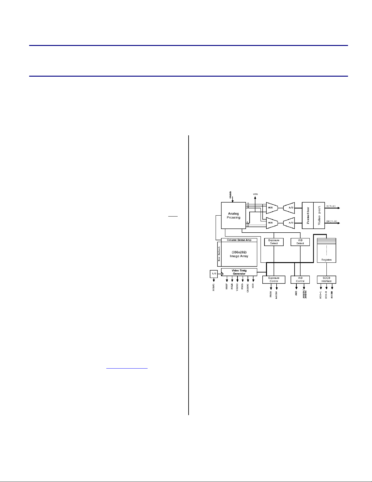
way been accessed by the ADSP-BF535
Processor see the schematic of the required
output pins in figure 2.1. The datasheet for the
OV6630 can be found at www.ovt.com
As it can be seen in figure 2.1 the pins Y[7:0]
and UV[7:0] are required to transfer data. The
PCLK represents the clock aligned to the data.
Each raising edge of the PCLK will indicate
valid data on the bus. These pins are necessary
and must be linked to the ADSP-BF535 for data
transfers. Additionally, some pins are required
for device control and configuration purposes.
The pin HREF asserted (polarity can be chosen)
indicates active video pixels (image data).
Figure 2.1
Because of the programmable sensor size as it is
discussed below HREF provides a way to
distinguish between active video pixels and
blank data. The blank data of the modified senor
field will also be transferred and is represented
by hex “10” on Y[7:0] and hex “80” UV[7:0].
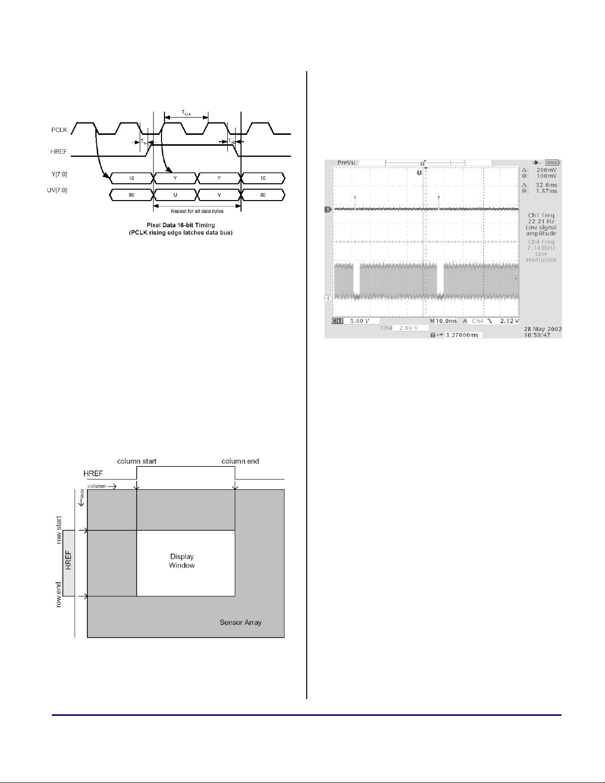
Figure 2.2 shows a transfer of one pixel,
blanking and HREF indicating an active pixel.
Due to the configuration the sensor is set to
output over a 16 -bit bus in this note. One pixel
exists of one byte of luminance and one byte of
Copyright 2003, Analog Devices, Inc. All rights reserved. Analog Devices assumes no responsibility for customer product design or the use or application of
customers’ products or for any infringements of patents or rights of others which may result from Analog Devices assistance. All trademarks and logos are property
of their respective holders. Information furnished by Analog Devices Applications and Development Tools Engineers is believed to be accurate and reliable, however
no responsibility is assumed by Analog Devices regarding technical accuracy and topicality of the content provided in Analog Devices’ Engineer-to-Engineer Notes.

a
chrominance information that can be transferred
the same time.
Figure 2.2
The windowing feature of the OV6630 image
sensors allows user-definable window sizing as
required by the application. Window size setting
(in pixels) ranges from 2 x 2 to 356 x 292, and
can be positioned anywhere inside the 356 x 292
boundary.
Note that modifying window size and/or position
does not change frame or data rate. The OV6630
imager alters the assertion of the HREF signal to
be consistent with the programmed horizontal
and vertical region. The default output window is
352 x 288. Figure 2.3 shows it graphically.
the VSYNC pin on channel 1 and the HREF pin
on channel 4. It can be seen if the sensor is set to
transfer e.g. 200 lines the HREF will be asserted
200 times also. Each start of frame will be
indicated by VSYNC around 2 ms before HREF
asserts.
Figure 2.4
The video output port of the OV6630 image
sensor provides a number of output format /
standard options to suit many different
application requirements. These formats are user
programmable through Omnivision’s SCCB two
wire control interface.
The OV6630 imager supports both ITU-601 and
ITU-656 output formats in different
configurations.
In this note the sensor is set to provide
differential video signals (YUV) 4:2:2, 16-bit
wide and clocked at 8.867MHz (PCLK).
3 Asynchronize Interface of the ADSP-BF535 Blackfin Processor
The Processors asynchronous interface is used to
receive the video data. 32-bit data can be fetched
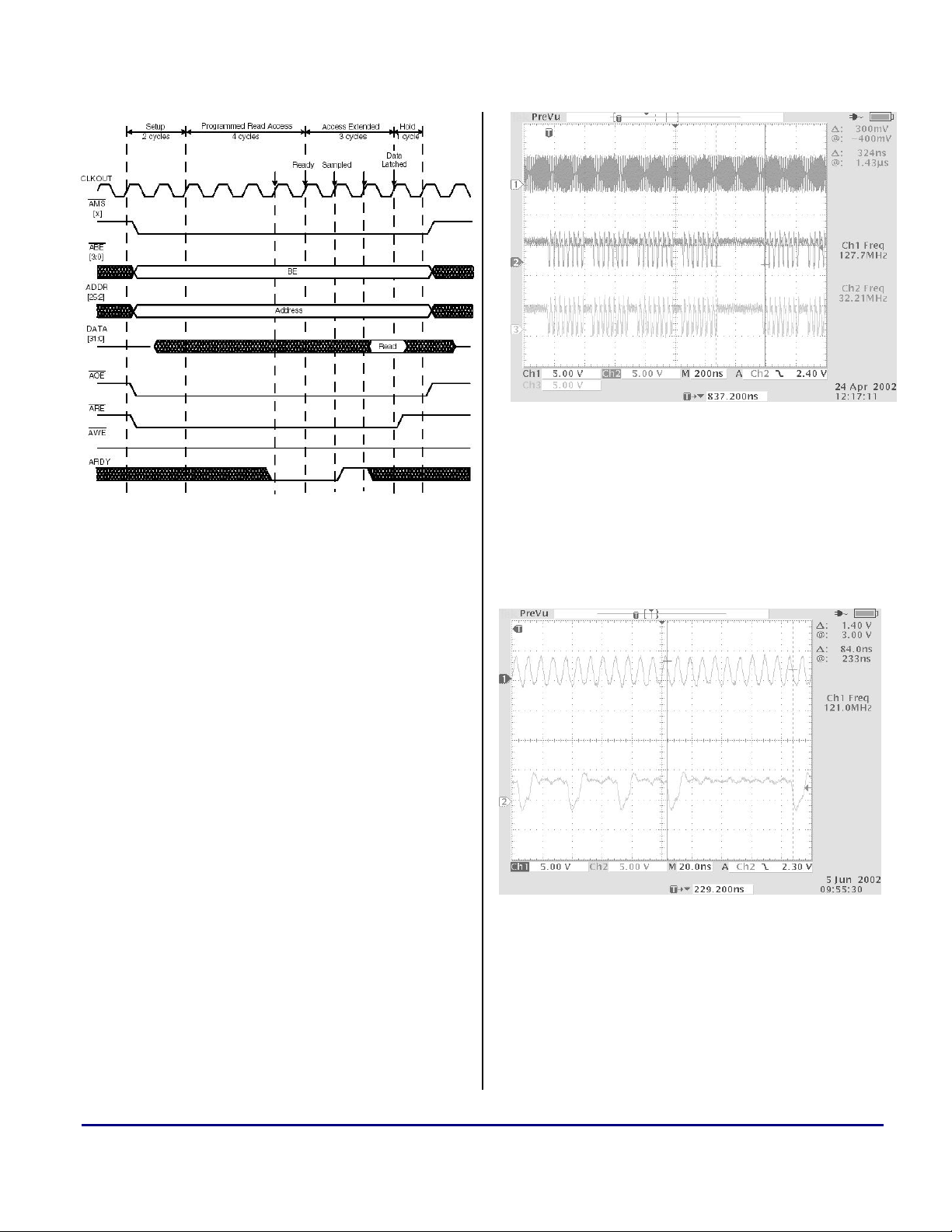
in a manner it is shown in figure 3.1.
Figure 2.3
In order to detect the first line of each frame the
signal VSYNC asserts before. Figure 2.4 shows
Interfacing the ADSP-BF535 Blackfin® Processor to Single-CHIP CIF Digital Camera "OV6630" over the External
Memory Bus (EE-181) Page 2 of 10

Figure 3.1
As mentioned in the ADSP-BF535 Blackfin
Hardware Reference Manual after a read cycle is
initiated the Async Memory Select line (/AMS) ,
Async Ouput Enable line (/AOE) and the Async
Read Enable line (/ARE) become asserted. After
a multicycle “Read Access” delay (Configured
by the Async Interface Bank Control Register),
the /ARE pin normally de-assert to complete the
read operation. But if the interface is configured
to extend the access, the /ARE pin remains low
until the ARDY pin has been sampled high. The
data will be fetched one cycle after this
happened.
a
Figure 3.2
Note also that each DMA transfer is split into
bursts of eight accesses (in this configuration,
four bursts per DMA execution). Understanding
this behavior is crucial for developing a proper
DMA interface. Figure 3.3 zooms into one of
these burst patterns to analyze how many cycles
are taken for each access.
Due to the architecture of the ADSP-BF535, a
DMA-controlled data download is somewhat
non-intuitive. Each data transfer is split into
bursts of eight read access. After the burst, a gap
appears because of internal bus activity. Figure
3.2 illustrates this.
As shown in the figure, the first DMA is set up to
read 32 data words (shown as Channel 2, the
/ARE signal). The large gap before the next
DMA is required for loading the next DMA
descriptor.
Interfacing the ADSP-BF535 Blackfin® Processor to Single-CHIP CIF Digital Camera "OV6630" over the External
Memory Bus (EE-181) Page 3 of 10
Figure 3.3
The peripheral clock “SCLK” is displayed in
channel 1 and channel 2 shows the /ARE pin.
After eight read strobes are done nine extra
cycles are taken to place the data into internal
memory.

a
4 Interface the ADSP-BF535 Processor into the OV6630
The ADSP-BF535 is configured to make full use
of its 32-bit external memory interface, in order
to gain maximum throughput. Two 16-bit words
from the camera will be packed into one 32-bit
word before being read by the Blackfin
Processor.
To interface to the single-chip camera,
LVT16374 latches are used. These parts are able
to fetch the data received from the video device
and latch it until the Asynchronous Interface has
been read.
The 8.867 MHz PCLK of the OV6630 clocks a
74HC74 configured as a /2 divider. The 4.43
MHz output then clocks an LVT16374 to fetch
the data transmitted by Y[7:0] and UV[7:0] at the
rising edge. The data will be held in the
LVT16374 until the next rising edge of the
CLOCK “CK” appears.
When /OE asserts, the Processor reads the data
latched by the LVT16374.
The ADSP-BF535 provides 256kBytes of
internal L2 Memory. One frame of CIF video
contains 352 X 288 pixels. Each pixel can be
represented in two bytes under the 4:2:2 digital
component video representation. This equates to
202,752 bytes per frame. As shown in Figure 5.2,
storing the blanking data as well would
obviously cause the memory to overflow.
The use of the AND gate shown in Figure 4.1
stops the data transfer to avoid storing blanking
data to the internal memory. The AND gate is
controlled by the HREF signal of the camera.
HREF remains high during active video
transfers. The memory will be filled just with
active video data.
To detect the first line of each frame, the
VSYNC signal can be used as mentioned in
section 2. VSYNC is connected to a
programmable flag and generates an interrupt
before the start of a frame. This interrupt will
enable the DMA transfer.
Figure 5.1 shows how the timing requirements of
the camera and the Processor are met.
The ARDY pin is used to synchronize the video
data with the ADSP-BF535. As long as the
ARDY pin is low, the access is held off? This
way, the camera is able to control the
asynchronous memory interface.
By routing a GPIO pin to the PWDN pin of the
OV6630, the sensor can be turned off without the
lose of configurations done during setup time by
the SCCB bus.
By routing a GPIO pin to the PWDN pin of the
OV6630, the sensor can be turned off without the
lose of configurations done during setup time by
the SCCB bus.
5 Data Structure and Improvements
As mentioned in section 2, the camera sends
active data plus blanking data sequentially.
Blanking data does fill the internal memory but
doesn’t contain any useful information.
Interfacing the ADSP-BF535 Blackfin® Processor to Single-CHIP CIF Digital Camera "OV6630" over the External
Memory Bus (EE-181) Page 4 of 10

a
Figure 4.1
Interfacing the ADSP-BF535 Blackfin® Processor to Single-CHIP CIF Digital Camera "OV6630" over the External
Memory Bus (EE-181) Page 5 of 10

a
f
f
f
f
A
At the raising edge
of PCLCK video
data can be taken
PCLCK = 8.867 MHz
OV6630
OV6630 Data Port
Y[7:0]
74HC74 [Q0] to
Top LVT16374 [CK]
74HC74 [Q0/] to
Bottom LVT16374 [CK]
ARDY
To half the frequency
each raising edge o
PCLCK will change the
state of the FlipFlops
output “74HC74”.
4.43 MHz
Each rising edge o
74HC74s Q & /Q will
fetch data to the certain
latch.
AOE/
Top LVT16374 Q[15:0]
To DSP D[15:0]
Each rising edge o
74HC74s Q & /Q will
put data to the output
/AOE remains low until
Figure 5.1
Each rising edge o
/AOE will fetch 32 bits
of data into the DS
P
ARDY is sampled high
fter each read burst one
access takes longer. That
does not affect the transfer
Interfacing the ADSP-BF535 Blackfin® Processor to Single-CHIP CIF Digital Camera "OV6630" over the External
Memory Bus (EE-181) Page 6 of 10

a
Figure 5.2
Interfacing the ADSP-BF535 Blackfin® Processor to Single-CHIP CIF Digital Camera "OV6630" over the External
Memory Bus (EE-181) Page 7 of 10

a
Conclusion:
The goal of this project is to show how video
sources can be connected to the ADSP-BF535
with less glue logic as possible. In fact, the
maximum resolution that can be achieved is
video in formats up to CIF (352 x 288). The
actual resolution is limited due to the limitation
of Blackfins external port timing, the DMA
structure and the internal memory.
The external port halts during the I/O processor
loads the next DMA descriptor when it has been
expired. That causes a large gap in the timing
(mentioned in chapter 3) and would not meet the
requirement set by the camera. A way out of this
problem is to set up the DMA downloading each
frame separately. So a DMA expires after
receiving each frame and will be reloaded during
the camera send blank data anyway (The camera
sends blank data between each line and each
frame).
The DMA Word Count Register is limited to the
maximum of 65,536 (2^16). A frame of CIF
format video in 4:2:2 standard is represented by
202,752 bytes (352*288 pixels * 2 bytes) . The
Processor accesses over a 32-bit interface results
in 50,688 words (202,752bytes /4 (bytes/word)).
That fits in the DMAs Word Count Register.
Resolutions higher than CIF could probably not
be served by the DMA on a frame by frame
basis. That causes the DMA to become reloaded
during active video pixel transfers and results in
data misses.
Building an interface like it is done in this note
the access to SDRAM or SRAM is not supported
anymore. Except the use of the PCI, SPORT, SPI
and USB data can just be stored in L1 or L2
memory. The ADSP-BF535 provides 52k of L1
memory and 256k bytes of L2 memory. L2
memory is be able to keep one frame of video in
CIF consisting of 202,752 bytes. Higher
resolutions does not fit in it.
A picture of the system is shown in figure C1.
Video transfers with higher resolutions
L
than CIF it is revered to the Note:
“Interfacing the ADSP-BF535 to
ADV7185/3 NTSC/PAL video decoder
over the External Memory Bus”.
This Note is available soon.
Interfacing the ADSP-BF535 Blackfin® Processor to Single-CHIP CIF Digital Camera "OV6630" over the External
Memory Bus (EE-181) Page 8 of 10

a
Figure C1
References:
-www.ovt.com
-OV6630 Datasheet
-OV7610MD Eva Board
-ADSP-BF535 Datasheet
-ADSP-BF535 Blackfin DSP Hardware Reference
-VisualDSP++™ 3.0
Interfacing the ADSP-BF535 Blackfin® Processor to Single-CHIP CIF Digital Camera "OV6630" over the External
Memory Bus (EE-181) Page 9 of 10

a
Document History
Version Description
April 17, 2003 Ported code example to VisualDSP++ 3.1
Changed according to new Blackfin naming convention.
January 23, 2003 Typos. Schematics, Gerber files and PDFs are attached to the web site
January 09, 2003 Initial release
August 06, 2002 Rev. 0.2
Interfacing the ADSP-BF535 Blackfin® Processor to Single-CHIP CIF Digital Camera "OV6630" over the External
Memory Bus (EE-181) Page 10 of 10
 Loading...