

Page 1

Engineer To Engineer Note EE-177
Technical Notes on using Analog Devices' DSP components and development tools
a
SHARC SPI Booting
Contributed by B. Mitchell and M. Walsh February 27, 2003
Contact our technical support by phone: (800) ANALOG-D or e-mail: dsp.support@analog.com
Or visit our on-line resources http://www.analog.com/dsp and http://www.analog.com/dsp/EZAnswers
Introduction
Upon power-up, the ADSP-21161 can be bootloaded as an SPI slave device. Although the
hardware interface is simple, there is a
complication that arises when using this boot
scheme. The SPI protocol does not provide an
obvious way for the booting, SPI-slave to
“pause” the boot-stream being transmitted by the
SPI-master device. This causes a problem when
SPI-booting because when performing “zeroinitializations”, the DSP executes code rather
than emptying the SPIRX buffer of the slave
DSP.
To save space in the .LDR file, sections of
memory with a large number of contiguous zeros
are truncated: Instead of storing these zeros in
the .LDR file, the loader only includes the
destination address and the number of zeros
required. (Consecutive zeros often occur because
of unitialized data arrays or several (5)
consecutive
which is
upon identifying one of these zero-init sections,
simply runs a small loop to write zeros to each
address specified. If the core stays in this loop
for a too long while the SPI-Master device
continues to transmit, then the 2-deep SPI FIFO
may overflow, and data may be lost. This EEnote describes three ways to avert this potential
problem.
“nop;” instructions, the opcode for
0x000000000000.) The kernel then,
Hardware Solution
There are two ways to pause the SPI master
device by implementing a HW feedback scheme,
either using a fifth pin as a FLAG signal, or
using the MISO pin. In both scenarios the DSP
would drive a hand-shake signal back to the SPImaster. This signal should be connected to a Flag
or Interrupt pin on the SPI-master. The SPImaster would monitor this FLAG or Interrupt
pin, and pause transmission when necessary.
Similarly, the feedback signal may also be
interpreted by the host as a “start transmission”
signal. Regardless of the protocol, implementing
a solution in HW would require a small change
to the loader kernel, 161_SPI.asm as well.
Described below is the former case, where the
feedback signal indicates that the SPI-master
should “pause” transmission. In the loaderkernel, the small sections of code that performs
the zero initializations are simply modified to
drive an output flag pin low until it finishes
executing the zero-initialization loop. The
before and after modification can be seen in
Listing-1 and Listing-2.
Copyright 2003, Analog Devices, Inc. All rights reserved. Analog Devices assumes no responsibility for customer product design or the use or application of
customers’ products or for any infringements of patents or rights of others which may result from Analog Devices assistance. All trademarks and logos are
property of their respective holders. Information furnished by Analog Devices Applications and Development Tools Engineers is believed to be accurate and
reliable, however no responsibility is assumed by Analog Devices regarding the technical accuracy and topicality of the content provided in all Analog Devices’
Engineer-to-Engineer Notes.
Page 2
DM_zero:
K
R0=R0-R0, I0=R3; //r0=0& I0=address
//as held in R3.
LCNTR=R2, DO dm_zero.end UNTIL LCE;
dm_zero.end:
DM(I0,M6)=R0;
JUMP read_boot_info;
Listing-1. Standard Zero-init code from SPI bootloader kernel, 161_SPI.asm
#include <def21161.h>
R0=R0-R0,I0=R3; //r0=0 & I0=address
//as held in R3.
USTAT1=DM(IOFLAG);
BIT SET USTAT1 FLG4O; //make output
dm(IOFLAG)=USTAT1;
BIT CLR USTAT1 FLG4; //flag4 = low
dm(IOFLAG)=USTAT1;
LCNTR=R2, DO dm_zero.end UNTIL LCE;
dm_zero.end:
DM(I0,M6)=R0;
BIT SET USTAT1 FLG4; //flag4 = high
dm(IOFLAG)=USTAT1;
JUMP read_boot_info;
Listing-2. Zero-init code with HW feedback added
using DSP Flag 4.
Included with this application note is a version of
the kernel modified in the manner described in
this section, as well as a project to be used on a
master ADSP-21161 to boot a slave in this
manner. It is important to note that when the
master is “paused”, care must be taken to ensure
that the transmission stops only after an entire
word has been sent. In the case of the ADSP21161, this will cause the host to need to resend
the last two words before the pause occurred.
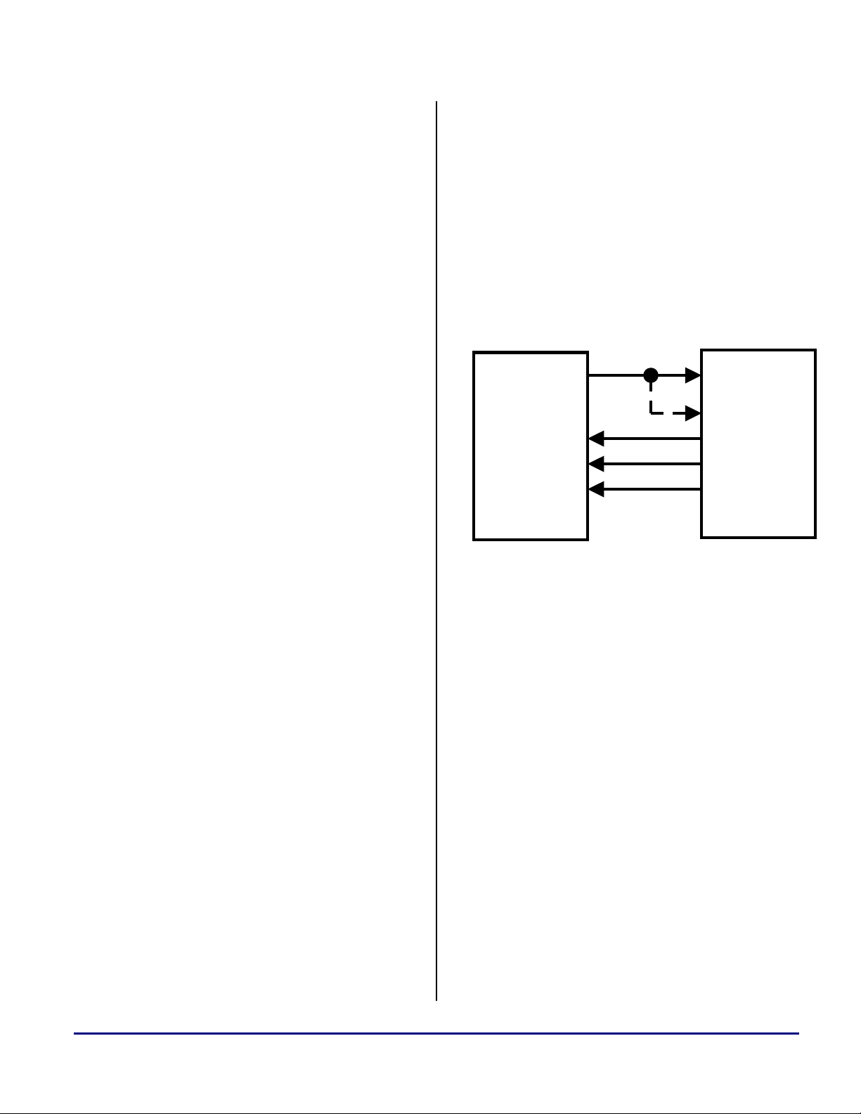
Alternatively, as shown in Figure-1, the slave
DSP’s MISO pin may be connected to the
Flag/Interrupt pin of the SPI-master. The DSP’s
SPI port may then transmit all 1’s or all 0’s
a
depending on the protocol implemented. The
SENDZ bit of the SPICTL register determines
what is sent when the DSP’s transmit buffer is
not refilled. If SENDZ is cleared, then the SPI
port will continue to retransmit the last word
written to the SPITX buffer. If SENDZ is set,
then the MISO pin will be driven low (sending
zeros) until a new word is written to the SPITX
buffer.
ADSP-21161 SPI-Master
MISO
MOSI
SPICL
SPIDS
Figure-1. Hardware feedback mechanism using the
DSP’s MISO pin.
The modifications to the loader kernel would be
similar to those in Listing-4. The actual code is
dependant on the host, and whether logic high or
logic low means “pause” or “resume”. In either
case, the code would write a data-word to the
SPITX register, rather than toggling a flag. This
word may be all ones, all zeros, or some other
mix to shape the waveform accordingly.
In this second implementation, where the MISO
pin is used as a handshake signal and as a dataline would require some software modifications
on the SPI-master side. This software would
need to be configured to monitor the flag-in
(handshake) pin in certain circumstances (during
booting), and then ignore it in others (when it is
receiving data over the MISO pin).
FLAG_IN
MISO
MOSI
SPICLK
SPIDS
SHARC SPI Booting (EE-177)
Page 2 of 20
Page 3

a
Software solution
Alternatively, the SPI-master device may insert
pauses on it’s own, without any feedback from
the booting slave device. The .LDR file which is
produced by the VisualDSP Loader is divided
into multiple “initialization sections”. Each
piece of contiguous, homogeneous data from the
executable is grouped together and given a threeword descriptive header. This header and
following data make up an “initialization
section”. The initialization header is used by the
loader kernel to correctly initialize the
subsequent data, and can also be used by the SPImaster to throttle the boot-stream when
necessary. The header is made of three words:
the WORD COUNT, the destination ADDRESS,
and finally a TAG identifying the data-type.
Listing-3 shows the 27 different data-types that
the loader uses:
0x00 FINAL_INIT
0x01 ZERO_DM16
0X02 ZERO_DM32
0x03 ZERO_DM40
0x04 INIT_DM16
0x05 INIT_DM32
0x06 INIT_DM40
0x07 ZERO_PM16
0x08 ZERO_PM32
0x09 ZERO_PM40
0x0A ZERO_PM48
0x0B INIT_PM16
0x0C INIT_PM32
0x0D INIT_PM40
0x0E INIT_PM48
0x0F ZERO_DM64
0x10 INIT_DM64
0x11 ZERO_PM64
0x12 INIT_PM64
0x13 INIT_PM8_EXT
0X14 INIT_PM16_EXT
0X15 INIT_PM32_EXT
0X16 INIT_PM48_EXT
SHARC SPI Booting (EE-177) Page 3 of 20
0X17 ZERO_PM8_EXT
0X18 ZERO_PM16_EXT
0X19 ZERO_PM32_EXT
0X1A ZERO_PM48_EXT
Listing-3. Loader TAG reference
For example, a typical initialization header is
shown in Listing-4.
0x00000013 // count
0x00040100 // addr
0x0000000e // tag
<data0>
<data1>
...
Listing-4. Example Initialization Header
Interpreting this header, the kernel would
recognize that there are 19 (0x13) instructions
that are located at address 0x40100. (The TAG of
0x0000000E signifies non-zero 48-bit PM data).
One way to implement a software solution
requires the SPI master device to read this
header. Instead of streaming the entire .LDR
image in one shot, it would send it one
initialization section at a time. It would read the
init-header and send the appropriate number of
words. The COUNT included in each init-header
can be used by the SPI master to figure out how
many words to “skip ahead” in the .LDR to find
the next init-header. When a header contains the
tag for one of the zero-initialization sections,
then the master should pause after sending the
header. Again, this is because these sections of
contiguous zeros are going to be initialized in
software by the loader kernel. The length of the
pause required is dependant upon the size of the
initialization section (the number of zeros to be
initialized) and the SPI baud rate. It takes one
DSP core cycle (10ns min) to for each zero
Page 4

a
initialization. If the SPI port were running at
10MHz (100ns), then it would take 320 core
SPI port. You will get an SPIRX buffer overflow
if more than two SPI words are received.
cycles for a single 32-bit word to arrive over the
Attachments
161_spi.asm
/* ==============================================================================
161_spi.asm
Serial Peripheral Interface compatible port based boot loader for the
ADSP21161 processor
Copyright (c) 2002 Analog Devices Inc. All rights reserved.
version 0.1 6/21/01 - Zero initializations and external memory sections
have not been tested. Check for newest version of the SPI kernel at
ftp.analog.com/pub/dsp/211xx/dev_tools/loader.
version 0.2 8/1/01 - All sections of kernel have been tested.
version 1.0 10/17/01 - R14 = 0xA001F81; was improperly initialized to
R14 = 0xA801F81; in the previous version of the kernel.
version 1.1 1/14/02 - changed some comments and fixed wait state init in
SDRAM init section
version 2.0 05.Sept.02 MSW
- Added initialization of all external memory types
-Added code to patch SPI IVT entry in final init
- Added final-init comments
- Added comments regarding tag info for each section
version 2.1 17.Oct.02 MSW
- Added comments regarding spi overflow errors possible during zero
initialization sections
- Added code to trap on spi overflow
version 2.2 20.DEC.2002 - M.Walsh
- Changed #define SDRAM 1 to #define SDRAM 0
SPI Feedback version 1.0 24.FEB.2003 - B.Mitchell
- Included feedback scheme described in EE-177
==============================================================================*/
#include <def21161.h>
#define SDRAM 1
.SECTION/PM seg_ldr;
nop; nop; nop; nop; // Reserved interrupt
SHARC SPI Booting (EE-177) Page 4 of 20
Page 5

a
reset:
nop; // - Instruction specified here is never executed. The core implicitly
// executes
// an IDLE instruction here until 256 instructions are booted. Once the
// kernel is booted, execution resumes at 0x40040 (the SPI Rx ISR). This
// address (0x40005) and the next (0x40006) are also used as a temporary
// buffer to DMA-in words from the SPI port
nop; // scratch memory2
//turn off SPI dma while kernel is executing
ustat1=dm(SPICTL);
bit clr ustat1 RDMAEN; //clear DMA bit in SPICTL
dm(SPICTL)=ustat1;
call user_init; // call subroutine at end of kernel in which users can insert
// initalization code, such as SDRAM, waitstates, etc.
R5=2; // used to decrement tag by two during loading.
L0=0; L1=0; L4=0; // Zero out L-registers so they can be used without wrap
L8=0; L12=0;L15=0; // ie. no circular buffering
M5=0;M6=1; // Setup M-registers to use for various memory transfers
M13=0; M14=1; M15=3;// use to load count in read_dma_info
I15 = 0x40006; // scratch DMA destination address for 32 bit words;
R14 = 0xA001F83; // sets up and enables SPI port with DMA,
// this is also the default setting
R11=DM(SYSCON); // Read current SYSCON setting
R12=PASS R11; // Hold Initial SYSCON setting
I12 = SYSCON; // Address of SYSCON
// ========================== READ_BOOT_INFO =======================================
// Places TAG in R8, Word Count in R2, and Destination Address in R3
// ----------------------------------------------------------------------------------read_boot_info:
call read_dma_info; // place two 48-bit words into 0x40004 and 0x40005
// equivalent to placing three 32-bit words into 0x40006,7,& 8
R2=dm(0x40006); //r2 passes section length
R3=dm(0x40007); //r3 passes destination address
SHARC SPI Booting (EE-177) Page 5 of 20
Page 6

a
R8=dm(0x40008); //r8 passes data-type tag
// -----------------------------------------------------------------------------------
// ========================== SPI Overflow Detect ====================================
// Monitor the SPI Status register to ensure that no overflow has ocurred. The RBSY
// (receiver busy) bit in SPI is set to 1 when the SPI port receive buffer is full and
// another word is clocked into the shift register. This may happen if the core is
// performing a zero-initialization section, and the SPI-master device continues to
// send data. RBSY is a sticky bit, so it will stay set until the spi port is
// disabled.
// If an overflow is detected the kernel will trap in an infinite loop so that user
// intervention can determine the problem. If this problem occurs, the SPI-master
// device must be configured to pause while the DSP performs the zero initializations.
// This can be done in software by looking at the .LDR section headers, or in hardware
// by configuring the kernel to set a DSP flag pin while it is performing zero// initializations. More information can be found in an EE note on the ADI website
// titled "21161 SPI Booting". http://www.analog.com/dsp
// ---------------------------------------------------------------------------------- USTAT1=DM(SPISTAT);
bit tst USTAT1 RBSY;
if tf JUMP (pc,0);
jump start_loader;
// ============================= FINAL_INIT =========================================
// This code is the very last piece run in the kernel. It uses a DMA to initialize the
// 256 instructions that reside in the interrupt vector table.
// ----------------------------------------------------------------------------------final_init:
R9=0xb16b0000; /* Load instruction PM(0,I8)=PX; */
R11=BSET R11 BY 9; /* Set IMDW to 1 for inst write */
DM(SYSCON)=R11; /* Setup for instruction write */
I4=0x40004; /* Point to 0x040004 for self modifing code*/
PX=pm(0x40004); /* Load instruction to be patched into 0x40040*/
I8=0x40040; /* Point to DMA8 vector to patch */
R9=pass R9, R11=R12; /* Clear AZ, hold initial SYSCON */
DO reset UNTIL EQ; /* set top of loop value to 0x40004 (see comments below)*/
PCSTK=0x40004; /* Set top of PC-stack, so RTI after final DMA goes to 0x40004;*/
//setup DMA parameters
DM(IMSRX)=M6; /* Set to increment internal ptr */
SHARC SPI Booting (EE-177) Page 6 of 20
Page 7

a
R1=0x40000; DM(IISRX)=R1; /* Setup DMA to load over ldr */
R2=0x180; DM(CSRX)=R2; /* Load internal count */
bit clr LIRPTL SPIRI; /* clear pending SPIRX interrupt latch */
bit set IMASK LPISUMI; // enable LPISUMI interrupt
bit set LIRPTL SPIRMSK; // enable SPI receive interrupt
bit set mode1 IRPTEN; // enable global interrupts
FLUSH CACHE; /* Flush cache for kernel overwrite */
DM(SPICTL)=R14; /* Start DMA transfer */
JUMP 0x40004 (DB); /* Jump to start */
IDLE; /* After IDLE, patch then start */
IMASK=0; /* clear IMASK on way to 0x40004 */
// When this final DMA completes, IDLE in the delayed branch completes, IMASK is cleared,
// and then the DSP executes the instruction at 0x40004. The loader automatically places the
// following instruction at that address:
// R0=R0-R0, DM(I4,M5)=R9, PM(I12,M13)=R11; //opcode: x39732D802000
// Executing this instruction performs the three things:
// 1) It sets the AN flag ("until EQ" now evaluates as true)
// 2) It restores the power-up value of SYSCON (held in R11).
// 3) It overwrites itself with the instruction PM(0,I8)=PX; (held in R9)
// Because the termination condition (EQ) is achieved within the last three instructions
// of the loop, the DSP jumps to the top-of-loop address one last time. We manually changed
// this top-of-loop address (PCSTK) to x40004, so, to conclude the kernel, the DSP executes
// the instruction at 0x40004 again. The new instruction there resets the DMA10 interrupt
// vector (x40050) to it's user-intended final value. At this point, the kernel is finished,
// and execution continues at 0x40005 as if nothing happened!
//
// ========================== END FINAL_INIT ==============================
// ========================== SPI Recieve DMA ISR ===========================
// This code must resolve to 0x40 in the interrupt vector table. If any code
// is added or removed prior to this without padding with "NOP's", then this
// kernel will not function.
nop;nop;nop;nop; // added nop's to resolve RTI to correct address
nop;nop;
x40040:
nop;
rti; // return to 0x40006 and begin executing kernel
// ========================== END SPI Recieve DMA ISR ======================
// ============================= START LOAD ========================================
// The following instructions analyze the TAG for each data section and initialize
// accordingly. READ_BOOT_INFO places the TAG in R8, Word Count in R2, and Destination
// Address in R3.
SHARC SPI Booting (EE-177) Page 7 of 20
Page 8

a
// Notes:
// - Several tags are initialized with common code to save space.
// - These instructions must execute sequentially because the tag value
// is decremented after each false test.
// ----------------------------------------------------------------------------------start_loader:
R0=PASS R8;
IF EQ jump final_init; // jump if tag = 0
//--------------- 1 0x0001 ZERO DM16 --------------//--------------- 2 0x0002 ZERO DM32 --------------test_dm_zero:
R0=R0-R5; // R5=2
IF GT JUMP (PC, test_dm40_zero);
dm_zero:
bit set mode2 FLG0O; //Set FLAG0 as an Output
bit clr flags FLG0; //Clear FLAG0 to pause SPI Host
R0=R0-R0, I0=R3; // clears r0 and sets I0 to R3
// which is the address information
LCNTR=R2, DO dm_zero.end UNTIL LCE;
dm_zero.end: DM(I0,M6)=R0; // writes zeros to dm memory; M6=1
bit set flags FLG0; //Set FLAG0 to continue boot data
JUMP read_boot_info;
// ---------------------------------------------------
//--------------- 3 0x0003 ZERO DM40 --------------test_dm40_zero:
R0=R0-1; // checks for tag zero dm40
IF NE JUMP (PC, test_dm_init);
dm40_zero:
bit set mode2 FLG0O; //Set FLAG0 as an Output
bit clr flags FLG0; //Clear FLAG0 to pause SPI Host
PX1=0;
PX2=0; // clears px
R0=R0-R0, I0=R3;
LCNTR=R2, DO dm40_zero.end UNTIL LCE;
dm40_zero.end: DM(I0,M6)=PX; // writes px out to correct memory locations
bit set flags FLG0; //Set FLAG0 to continue boot data
JUMP read_boot_info;
// -------------------------------------------------------
SHARC SPI Booting (EE-177) Page 8 of 20
Page 9

//--------------- 4 0x0004 INIT DM16 --------------//--------------- 5 0x0005 INIT DM32 --------------test_dm_init:
R0=R0-R5; // checks for tag init dm16
IF GT JUMP (PC, test_dm40_init);
dm_init:
B0=R3;
LCNTR=R2, DO dm16_init.end UNTIL LCE;
CALL read_SPI_word;
DM(I0,M6)=R8;
NOP;
dm16_init.end:NOP; //a call can't be in the last 3 instructions
JUMP read_boot_info;
// -------------------------------------------------------
//--------------- 6 0x0006 INIT DM40 --------------test_dm40_init:
R0=R0-1; // checks for tag init dm40
IF NE JUMP (PC, test_pm_zero);
dm40_init:
B0=R3;
LCNTR=R2, DO dm40_init.end UNTIL LCE;
CALL read_dma_info;
PX=dm(0x40004);
dm(i0,M6)=PX;
PX=dm(0x40005);
dm40_init.end:dm(i0,M6)=PX;
JUMP read_boot_info;
// -------------------------------------------------------
//--------------- 7 0x0007 ZERO PM16 --------------//--------------- 8 0x0008 ZERO PM32 --------------//--------------- 9 0x0009 ZERO PM40 --------------//--------------- 10 0x000A ZERO PM48 --------------test_pm_zero:
R0=R0-R5; // R5=2, checks for tag zero pm16, zero pm32
IF LE JUMP (PC, dm_zero);
R0=R0-R5; // R5=2, checks for tag zero pm40, zero 48
IF LE JUMP (PC, dm40_zero);
// -------------------------------------------------------
a
SHARC SPI Booting (EE-177) Page 9 of 20
Page 10

a
//--------------- 11 0x000B INIT PM16 --------------//--------------- 12 0x000C INIT PM32 --------------//--------------- 13 0x000D INIT PM40 --------------//--------------- 14 0x000E INIT PM48 --------------test_pm_init:
R0=R0-R5; // R5=2, checks for tag init pm16, init pm32
IF LE JUMP (PC, dm_init);
R0=R0-R5; // R5=2, checks for tag init pm40, init pm48
IF LE JUMP (PC, dm40_init);
// -------------------------------------------------------
//--------------- 15 0x000F ZERO DM64 --------------test_dm64_zero:
R0=R0-1;
IF NE JUMP (PC, test_dm64_init);
dm64_zero:
R2=R2+R2; //double count and initialize in NW memory
R3 = LSHIFT R3 by 1; //double longword address to NW memory
jump dm_zero;
//------------------------------------------------------------
//--------------- 16 0x0010 INIT DM64 --------------test_dm64_init: R0=R0-1;
IF NE JUMP (PC, test_pm64_zero);
dm64_init: I0=R3;
LCNTR=R2, DO dm64_init.end UNTIL LCE;
CALL read_SPI_word; /* read 32 lsbs of 64-bit word */
PX2=R8;
CALL read_SPI_word; /* read 32 msbs of 64-bit word */
PX1=R8;
nop;
nop; /* Call cannot be in last 3 instructions of loop */
dm64_init.end:DM(I0,M6)=PX (lw); /* write all 64-bits to longword address location */
JUMP read_boot_info;
//------------------------------------------------------------
//--------------- 17 0x0011 ZERO PM64 --------------//--------------- 18 0x0012 INIT PM64 --------------test_pm64_zero:
R0=R0-1;
IF EQ JUMP (PC, dm64_zero);
SHARC SPI Booting (EE-177) Page 10 of 20
Page 11

a
test_pm64_init:
R0=R0-1;
IF EQ JUMP (PC, dm64_init);
//------------------------------------------------------------
//=================================================================================
// "INIT PMx EXT" load "packed" instructions into external memory. External memory
// starts at address 0x200000 on the 21161. The format for this packing can be found
// in the Chapter 5 of the 21161 Hardware Reference. Zero-init code sections (many
// consecutive NOP's) are initialized using the EXT_ZERO_CODE subroutine above.
//----------------------------------------------------------------------------------
//--------------- 19 0x0013 INIT PM8 EXT --------------test_pm8_init_ext:
R0=R0-1; //checks for init pm8 ext tag
IF NE JUMP (PC, test_pm16_init_ext);
B0=R3;
R2=LSHIFT R2 by -1; // r2 was # 32-bit words -> two inits per loop, so half R2
LCNTR=R2, DO pm8_init.end UNTIL LCE;
CALL read_SPI_word; // r8 = B1 B2 B3 B4
lcntr=4, do loop8 until lce;
r8=rot r8 by 8; // rotate the 32 word left by 8 bits
loop8: DM(I0,M6)=R8; // to write out MSB (B1) first
CALL read_SPI_word; // r8 = B0 B0 B5 B6
DM(1,I0)=R8; // write out B6 to address n+1
R8=rot R8 by -8;
pm8_init.end:
DM(I0,4)=R8; // write out B5 to address N, and then leave two
// blank addresses to comply w/ 8-bit packing convention.
JUMP read_boot_info;
//------------------------------------------------------------
//--------------- 20 0X0014 INIT PM16 EXT --------------test_pm16_init_ext:
R0=R0-1; //checks for init pm16 ext tag
IF NE JUMP (PC, test_pm32_init_ext);
B0=R3;
R2=LSHIFT R2 by -1;
LCNTR=R2, DO pm16_init.end UNTIL LCE;
CALL read_SPI_word; // r8 = B1 B2 B3 B4
DM(1,I0)=R8; // write out b3, b4
R8=LSHIFT R8 by -16;
SHARC SPI Booting (EE-177) Page 11 of 20
Page 12

a
DM(I0,2)=R8; // write out b1, b2
CALL read_SPI_word; // r8 = B0 B0 B5 B6
DM(I0,2)=R8; // write out B5, b6, leave 1 black address
// for 16-bit packing
nop;
pm16_init.end: nop; // call can't be in last 3 instructions of loop
JUMP read_boot_info;
//------------------------------------------------------------
//--------------- 21 0X0015 INIT PM32 EXT --------------test_pm32_init_ext:
R0=R0-1;
IF NE JUMP (PC, test_pm48_init_ext);
B0=R3;
LCNTR=R2, DO pm32_init.end UNTIL LCE;
CALL read_SPI_word; // r8 = B1 B2 B3 B4, then R8 = B0 B0 B5 B6
DM(I0,M6)=R8;
nop;
pm32_init.end: nop; // a call can't be in the last 3 instructions
JUMP read_boot_info;
//------------------------------------------------------------
//--------------- 22 0X0016 INIT PM48 EXT --------------test_pm48_init_ext:
R0=R0-1; //checks for init pm48 ext tag
IF NE JUMP (PC, ext_zero_code);
// configure External port for 48-bit writes (disable linkports)
ustat1=dm(SYSCON);
bit set ustat1 IPACK0;
dm(SYSCON)=ustat1;
I8=R3;
lcntr=R2, do pm48_init.end until lce;
CALL read_dma_info; // get 2 instructions (three 32-bit words)
I6=0x40004;
LCNTR=0x2, do loop1 until lce;
PX=DM(I6,M6); // read word from internal scratch locations
R0=PX1; // swap px registers for external write
PX1=PX2; // (see pag 5-13 of the 161 HW-Ref Rev3.0)
SHARC SPI Booting (EE-177) Page 12 of 20
Page 13

a
PX2=R0;
loop1: PM(I8,M14)=px; //write word to external memory
pm48_init.end:nop; //nested loops can't terminate on the same instruction
jump read_boot_info;
//===========================================================================
//============================= EXT_ZERO_CODE =============================
// This portion of code is used to initialize external memory with zero's
// r0 holds (tag - 22)
// r2 holds number of external #NOP's to be initialized
// calculate how many external addresses are used by each NOP based on the tag:
// If pm8 (tag: 23 0X0017 ZERO PM8 EXT), r0 = 1, so multiply count by 8 (lshift r2 by 3)
// If pm16 (tag: 24 0X0018 ZERO PM16 EXT), r0 = 2, so multiply count by 4 (lshift r2 by 2)
// If pm32 (tag: 25 0X0019 ZERO PM32 EXT), r0 = 3, so multiply count by 2 (lshift r2 by 1)
// If pm48 (tag: 26 0X001A ZERO PM48 EXT), r0 = 4, so multiply count by 1 (lshift r2 by 0)
//-----------------------------------------------------------ext_zero_code:
r6=4;
r0=r6-r0, I0=R3; // calculate amount to shift by based on (4 - tag)
r2=lshift r2 by r0; // r2 = number addresses per NOP
LCNTR=R2, DO ext_zero_code.end UNTIL LCE;
ext_zero_code.end: DM(I0,M6)=M13; //m13=0
JUMP read_boot_info; //fetch header for next block
//===========================================================================
//============================= read_dma_info =============================
// This section performs a length 3, 32bit dma into scratch location
// that can be read out as 2 40 or 48 bit words
//-----------------------------------------------------------read_dma_info:
DM(IMSRX)=M14; /* setup up modify to 1*/
DM(CSRX)=M15; /* Setup DMA count to be 3 ~ 3 32 bit words = 2 48 bit words */
jump more;
//============================= read_SPI_word =============================
// This section reads ONE 32-bit spi word into a scratch location (0x40006)
// and then also into register R8
//-----------------------------------------------------------read_SPI_word:
DM(IMSRX)=M14; /* setup up modify to 1*/
DM(CSRX)=M14; /* Setup DMA count to be 1 */
more: DM(IISRX)=I15; /* Setup DMA destination address; I15 should be 0x40006*/
SHARC SPI Booting (EE-177) Page 13 of 20
Page 14

a
ustat1=dm(SPICTL);
bit set ustat1 RDMAEN;
dm(SPICTL)=ustat1;
SPI_DMA_not_done_yet: // Test SPI completion
R1 = DMA8ST;
R0 = DM(DMASTAT);
R0 = R0 AND R1;
IF NE jump SPI_DMA_not_done_yet;
ustat1=dm(SPICTL);
bit clr ustat1 RDMAEN;
dm(SPICTL)=ustat1;
r8=dm(0x40006);
rts;
// ============================= USER_INIT ========================================
// If any registers need initialization before the kernel begins importing the application,
// they should be done so here. Typically, a user would need to initialize SDRAM settings,
// but they may also modify WAIT, SYSCON, SPICTL, or LCTL to increase the speed of the boot
// process.
// This subroutine may include NO MORE THAN 48 instructions (in addition to the RTS). As
// modifications are made, "kernel.map" shows the updated number of remaining free locations
// under "Memory-Words-Unused".
// ----------------------------------------------------------------------------------user_init:
#if SDRAM
r0=0xFFFFF; // clear MSx waitstate and mode
dm(WAIT)=r0;
r0=900; // refresh rate
dm(SDRDIV)=r0;
r0=0x5114662; // SDRAM running @ Core-clock
dm(SDCTL)=r0;
#endif
// ~~~~~INSERT SYSTEM INITIALIZATION CODE HERE ~~~~
RTS; // return from user_init to loader_kernel_init
// ============================ END USER_INIT =====================================
// ============================ END 161_SPI =========================================
SHARC SPI Booting (EE-177) Page 14 of 20
Page 15

SPIhost.asm
/* ------------------------ SPIhost.asm -------------------------------------- Version 1.0 24.Feb.02 - B. Mitchell
This project is intended for a single ADSP-21161 processor.
This code is to be used to boot a slave ADSP-21161 while including a form
of SPI feedback as described in EE-177. Prior to any user modifications,
FLAG0 on the host DSP should be connected to the SPIDS pin on the slave,
and FLAG4 should be connected to FLAG0 on the slave DSP.
The boot data to be sent to the slave is contained in spiloader.ldr.
------------------------------------------------------------------------------*/
#include <def21161.h>
#define OFFSET 2 // Depth of FIFO on SPI buffer (# of words to resend)
/* Data section to host the loader file */
.section/dm seg_dmda;
.var master_tx_buf[] = "spiloader.ldr"; //kernel in 32-bit include format
/* Main code section */
.section/pm seg_pmco;
_main:
r0=0x00000000; // initially clear SPI control register
dm(SPICTL)=r0;
// Send the first 256 words (kernel) for the initial boot of the slave
r0=master_tx_buf; //configure index register for SPI transmit
dm(IISTX)=r0;
r0=0x180; //configure count register for SPI transmit
dm(CSTX)=r0;
r0=1; //configure modify register for SPI transmit
dm(IMSTX)=r0;
ustat1=0;
bit set ustat1 MS | WL32 | BAUDR1 | SPTINT | SPIEN | TDMAEN | FLS0 | PSSE;
dm(SPICTL) = ustat1; // start transfer by configuring SPICTL
/* Wait for the kernel to finish transferring */
lcntr=3, do later until lce;
a
SHARC SPI Booting (EE-177) Page 15 of 20
Page 16

a
wait: lcntr=0xffffff;
do (pc,1) until LCE;
nop;
later: nop;
r0=0x00000000; // clear SPI control register before reinitializing
dm(SPICTL)=r0;
// No need to reconfigure the IISTX register, DMA will continue where it left off.
r0= @master_tx_buf - 0x180; // configure count register for SPI transmit
dm(CSTX)=r0;
r0=1; // configure modify register for SPI transmit
dm(IMSTX)=r0;
ustat1=0;
bit set ustat1 MS | WL32 | BAUDR1 | SPTINT | SPIEN | TDMAEN | FLS0 | PSSE;
dm(SPICTL) = ustat1; // start transfer by configuring SPICTL
// Watch for FLAG4 to go low indicating that the slave has entered a zero init section.
waiting_for_pause:
ustat1=dm(IOFLAG);
bit tst ustat1 FLG4;
if not tf jump stop_spi;
waiting_for_pause.end: jump waiting_for_pause;
_main.end:
// End of code, stay here forever.
waiter: nop;
jump waiter;
waiter.end:
// Pause SPI transmission until the slave is ready.
stop_spi:
bit clr lirptl SPITI; // Clear any pending SPITX interrupt
r1=dm(CSTX); // Save count register
r2=dm(IISTX); // Save index register
r3=1;
SHARC SPI Booting (EE-177) Page 16 of 20
Page 17

a
dm(CSTX)=r3; // Set DMA count register to 1 to stop DMA
bit set lirptl SPITMSK;
bit set imask LPISUMI;
bit set mode1 IRPTEN; // Unmask SPITX interrupt.
// Update the count and index registers to reflect the two words that will be lost.
r4=OFFSET; r1=r1+r4; r2=r2-r4; nop;
idle; // Wait for the SPI transmission to finish
r0 = 0; //Disable the SPI
dm(SPICTL) = r0;
r10=0;
ustat1=dm(IOFLAG); //Monitor FLAG4 to know when the slave is ready
r10=r10+1; // Count how long the slave is holding off transmission.
bit tst ustat1 FLG4;
if not tf jump (pc,-3);
dm(CSTX)=r1; // Reload the DMA control registers with corrected values.
dm(IISTX)=r2;
ustat1 = dm(SPICTL); //Reenable SPI Transmission
bit set ustat1 MS | WL32 | BAUDR1 | SPTINT | SPIEN | TDMAEN | FLS0 | PSSE;
dm(SPICTL) = ustat1;
jump waiter;
stop_spi.end:
.section/pm seg_rth;
// Run-time header, code starts here.
nop; nop; nop; nop;
Chip_Reset:
idle;
jump _main;
nop; nop;
.global spi_tx_isr;
//SPI interrupt vector, automatically placed in correct position in LDF file
spi_tx_isr:
r15=0xfffff;
SHARC SPI Booting (EE-177) Page 17 of 20
Page 18

a
rti;
spi_tx_isr.end:
/*----------------------------- End of SPIhost.asm ----------------------------------*/
SPIhost.ldf
/* --------------------------------------------------------------------------- host.ldf – version 1.0 – 24.Feb.2003
LDF File to accompany SPIhost project.
-----------------------------------------------------------------------------*/
ARCHITECTURE(ADSP-21161)
//
// ADSP-21161 Memory Map:
// -----------------------------------------------// Internal memory 0x0000 0000 to 0x000f ffff
// -----------------------------------------------// 0x0000 0000 to 0x0001 ffff IOP Regs
// Block 0 0x0002 0000 to 0x0002 1fff Long Word (64) Addresses
// 0x0002 2000 to 0x0002 7fff (reserved)
// Block 1 0x0002 8000 to 0x0002 9fff Long Word (64) Addresses
// 0x0002 a000 to 0x0003 ffff (reserved)
// Block 0 0x0004 0000 to 0x0004 3fff Normal Word (32/48) Addresses
// 0x0004 4000 to 0x0004 ffff (reserved)
// Block 1 0x0005 0000 to 0x0005 3fff Normal Word (32/48) Addresses
// 0x0005 4000 to 0x0007 ffff (reserved)
// Block 0 0x0008 0000 to 0x0008 7fff Short Word (16) Addresses
// 0x0008 8000 to 0x0009 ffff (reserved)
// Block 1 0x000a 0000 to 0x000a 7fff Short Word (16) Addresses
// 0x000a 8000 to 0x000f ffff (reserved)
// -----------------------------------------------// Multiproc memory 0x0010 0000 to 0x007f ffff
// -----------------------------------------------// 0x0010 0000 to 0x0011 ffff Hammerhead ID=001 Internal memory
// 0x0012 0000 to 0x0013 ffff Hammerhead ID=010 Internal memory
// 0x0014 0000 to 0x0015 ffff Hammerhead ID=011 Internal memory
// 0x0016 0000 to 0x0017 ffff Hammerhead ID=100 Internal memory
// 0x0018 0000 to 0x0019 ffff Hammerhead ID=101 Internal memory
SHARC SPI Booting (EE-177) Page 18 of 20
Page 19

a
// 0x001a 0000 to 0x001b ffff Hammerhead ID=110 Internal memory
// 0x001c 0000 to 0x001f ffff Hammerhead ID=all Internal memory
// -----------------------------------------------// External memory 0x0020 0000 to 0xffff ffff
// ------------------------------------------------
$OBJECTS1 = $COMMAND_LINE_OBJECTS;
PROCESSOR master
{
OUTPUT( $COMMAND_LINE_OUTPUT_FILE )
MEMORY {
//block0
mem_ivt { TYPE(PM RAM) START(0x00040000) END(0x000400ff) WIDTH(48) }
mem_pmco { TYPE(PM RAM) START(0x00040100) END(0x00040fff) WIDTH(48) }
mem_b1 { TYPE(DM RAM) START(0x00050100) END(0x00053FFF) WIDTH(32) }
//external memory
mem_sdram { TYPE(DM RAM) START(0x00200000) END(0x002fffff) WIDTH(32) }
}
RESOLVE (spi_tx_isr, 0x40044)
SECTIONS {
// map .sections defined in code to memory ranges
dxe_ivt {
INPUT_SECTIONS( $OBJECTS1(seg_rth) )
} > mem_ivt
dxe_pmco { INPUT_SECTIONS( $OBJECTS1(seg_pmco) ) } > mem_pmco
dxe_b1 { INPUT_SECTIONS( $OBJECTS1(seg_dmda) ) } > mem_b1
dxe_sdram { INPUT_SECTIONS( $OBJECTS1(sdram_sec)) } > mem_sdram
}
}
/* -------------------------------- End of SPIhost.ldf ----------------------------*/
SHARC SPI Booting (EE-177) Page 19 of 20
Page 20

Document History
Version Description
February 27, 2003 by B. Mitchell Included code for both the kernel and the host.
November 5, 2002 by M. Walsh Initial Release
a
SHARC SPI Booting (EE-177) Page 20 of 20
 Loading...