

Page 1

Engineer To Engineer Note EE-172
s
a
Technical Notes on using Analog Devices' DSP components and development tools
Contact our technical support by phone: (800) ANALOG-D or e-mail: dsp.support@analog.com
Or vi sit ou r on-l ine re sourc es ht tp:// www.analog.com/dsp and http://www.analog.com/dsp/EZAnswer
Using the Dynamic Power Management Functionality of the ADSP-BF535
Blackfin® Processor
Contributed by Ching Lam May 13, 2003
Introduction
The ADSP-BF535 Blackfin® processor is ideal
for power-sensitive multimedia applications
because it provides support for a multi-tiered
approach to power management. That is, the
processing performance level can be tuned within
an application to maximize power savings.
The ADSP-BF535 Dynamic Power Management
functionality includes the following components:
• Software control of Core Clock (CCLK)
• Software control of System Clock (SCLK)
• Software control of the Phase Locked Loop
(PLL)
• Dynamic Voltage Control by interfacing to an
external voltage controller
Changes in operating voltage and frequency
result in significant savings in power
consumption. These savings can be modeled by
the following equation:
PR/PN=(FCR/FCN)(V
DDR/VDDN
where
• PR/PN is the ratio of reduced power to nominal
power
• FCN is the nominal core clock frequency
• F
• V
• V
• T
• T
Copyright 2003, Analog Devices, Inc. All rights reserved. Analog Devices assumes no responsibility for customer product design or the use or application of customers’
products or for any infringements of patents or rights of others which may result from Analog Devices assistance. All trademarks and logos are property of their
respective holders. Information furnished by Analog Devices Applications and Development Tools Engineers is believed to be accurate and reliable, however no
responsibility is assumed by Analog Devices regarding technical accuracy and topicality of the content provided in Analog Devices’ Engineer-to-Engineer Notes.
is the reduced core clock frequency
CR
is the nominal internal supply voltage
DDN
is the reduced internal supply voltage
DDR
is the duration running at FCR
FR
is the duration running at FCN
FN
)2(TFR/ TFN)
As an example, consider the following scenario:
• FCN = 300 MHz
• FCR = 100 MHz
• V
• V
DDN
DDR
= 1.5 V
= 1.0V
• TFR = 3
• TFN = 1
Thus,
(PR/PN)=(100/300)(1.0/1.5)²(3/1) = 0.44 Î
56% savings
Since Blackfin Processors not only have a
programmable operating frequency, but also
allow core voltage to be changed in concert with
frequency changes, less power will be consumed
when running a section of code at a lower
frequency and a lower voltage, even if execution
time is longer.
The remainder of this application note details how
the frequency can be modified on the ADSPBF535. In addition, an example of changing core
voltage on the ADSP-BF535 EZ-KIT Lite™ is
included. The ADSP-BF535 EZ-KIT Lite
provides a prototype capability to allow core
voltage changes by setting programmable flag
pins connected to an external power management
chip.
The data sheet for the ADSP-BF535
L
contains a frequency vs. voltage graph
outlining acceptable CCLK and
VddCore combinations. The data sheet
Page 2
a
must be reviewed prior to running your
application with different frequency and
voltage combinations.
Clock
The input clock, CLKIN, provides the necessary
clock frequency to allow for the derivation of the
core clock (CCLK) and system clock (SCLK)
frequencies. The ADSP-BF535 has external pins
that are sampled on reset to determine a
multiplication factor (MSEL) and a divide factor
(SSEL). MSEL is used to determine the core
clock frequency (CCLK) and SSEL is used to
determine the system clock (SCLK) frequency.
Both of these values can additionally be
controlled by programming registers. CLKIN is
multiplied up by the MSEL value to obtain
CCLK. SSEL is used to divide down the CCLK
value to obtain SCLK.
CCLK is the core execution clock rate and SCLK
is used by the peripherals and external memory.
Control Register. The possible dividing factors
are 2, 2.5, 3, or 4.
Dynamic Power Management Controller
The Dynamic Power Management Controller
consists of two main components which allows
flexibility in managing power dissipation on the
ADSP-BF535:
• Operating Modes
• Peripheral Clocking
Operating Modes
Four different operating modes control the power
savings of the ADSP-BF535:
• Full-On Mode
• Active Mode
• Sleep Mode
• Deep Sleep Mode
Phase Locked Loop (PLL)
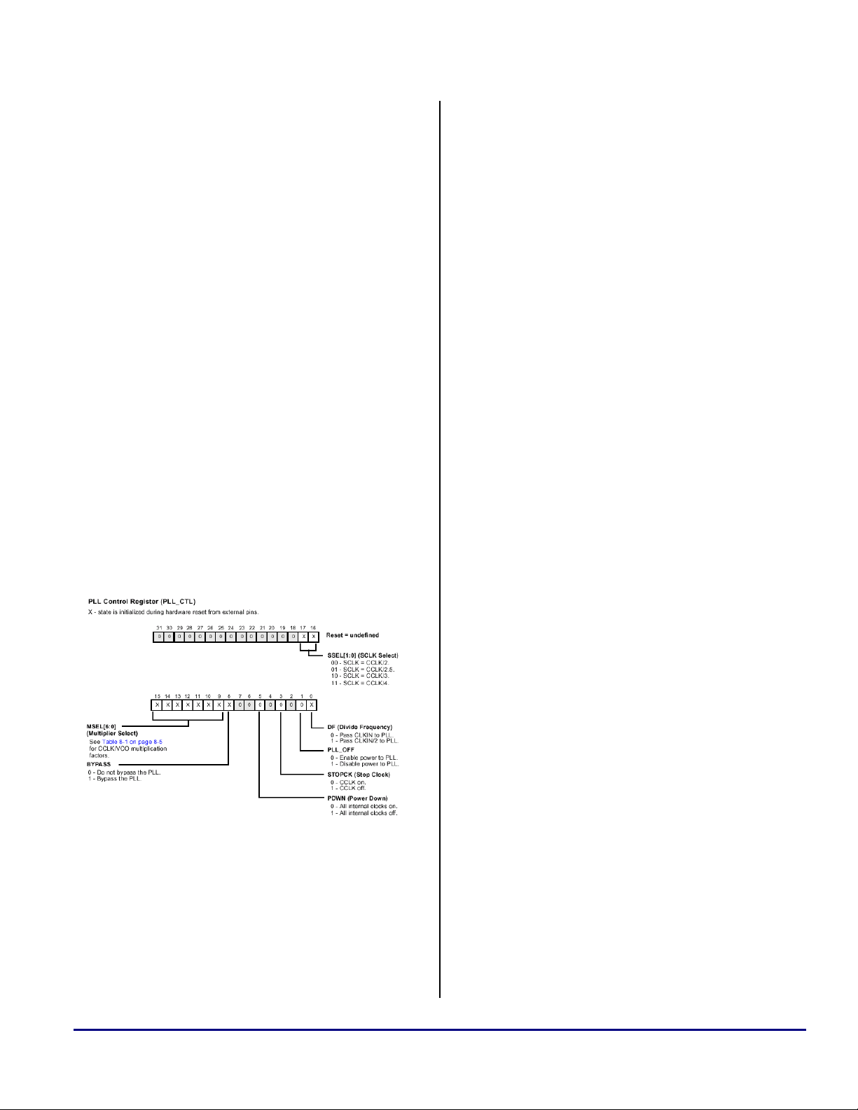
Figure 1. PLL Control Register (PLL_CTL)
The PLL provides a multiplying factor between
the ranges of 1 to 31 times the input clock,
CLKIN, by programming the MSEL bits in the
PLL Control Register. The PLL also supplies the
factor by which CCLK is divided to produce
SCLK by programming the SSEL bits in the PLL
Full-On Mode
In this mode, the PLL, CCLK, and SCLK are
enabled. However, the PLL is not in bypass.
This mode does not allow the CLKIN to CCLK
multiplying factor to be changed. From this
mode, the processor can transition to any of the
other three modes.
Active Mode
In this mode, the PLL, CCLK, and SCLK are
enabled. However, the PLL is in bypass as well.
This puts CCLK at one-half the value of CLKIN.
The option to disable the PLL in this mode is also
available. From this mode, the processor can
transition to any of the other three modes.
Sleep Mode
In this mode, the PLL and SCLK are enabled.
However, CCLK is disabled. Depending on the
previous state, the PLL could be bypassed or
Using the Dynamic Power Management Functionality of the ADSP-BF535 Blackfin® Processor (EE-172) Page 2 of 8
Page 3

a
enabled. Since CCLK is disabled, SCLK
continues to run at the previous state’s frequency.
From this mode, the processor can transition to
either Full-On Mode or Active Mode. A wakeup
event causes the processor to transition out of this
mode.
Deep Sleep Mode
In this mode, the PLL, CCLK, and SCLK are all
disabled. From this mode, the processor can
transition to the Active Mode through a Real
Time Clock interrupt. The processor can also
transition to either Full-On Mode or Active Mode
through a hardware reset.
Peripheral Clocking
In addition to the different operating modes
described above, the peripherals can be
individually enabled or disabled. By default, the
peripherals are all enabled. However, each
peripheral can be disabled by setting the
corresponding bit in the Peripheral Clock Enable
Register (PLL_IOCK).
modify the operating voltage of the ADSPBF535.
For the purpose of this EE-Note, only the
implementation on the ADSP-BF535 EZ-KIT
Lite will be discussed.
Implementation
As described above, there are four possible
operating modes to transition among. There are
also a range of operating voltages and frequencies
that the core can be programmed to run at. The
following sections will describe in detail how to
implement some of these mode, voltage, and
frequency transitions.
Changing Modes
To transition between the different operating
modes, a specific setup sequence must be
followed. The general procedure that should be
followed is:
1) Program the wakeup event to bring the core
out of idle mode.
2) Program the PLL.
3) Disable interrupts.
4) Flush the pipeline, and place the core into an
idle state.
5) Reinstate interrupts.
6) Transitioned into new mode.
Figure 2. Peripheral Clock Enable Register
Dynamic Voltage Control
The ADSP-BF535’s operating voltage can be
changed dynamically via two methods.
For the ADSP-BF535 EZ-KIT Lite, a prototype
solution has been implemented to dynamically
change the core voltage via three programmable
flag pins, PF12, PF13, and PF14.
For production silicon, an external programmable
voltage regulator, the ADP-3053, is available to
Using the Dynamic Power Management Functionality of the ADSP-BF535 Blackfin® Processor (EE-172) Page 3 of 8
Wakeup Events
The ADSP-BF535’s peripherals can be enabled to
generate a wakeup event to bring the core out of
an idle state. The System Interrupt WakeupEnable Register (SIC_IWR) configures which
peripherals are enabled to wakeup the core.
In the examples that follow, the software
watchdog timer will be used as the peripheral that
generates a wakeup event to the core.
Page 4

a
Upon reaching 0, the watchdog timer stops
counting. Depending on the value set for ICTL in
the Watchdog Control Register, an event could be
generated.
Figure 3. System Interrupt Wakeup-Enable Register
For this particular peripheral, there are three
additional registers to setup the watchdog timer
appropriately:
• Watchdog Count Register
• Watchdog Status Register
• Watchdog Control Register
Watchdog Count Register
The Watchdog Count Register (WDOG_CNT)
contains the count value for the watchdog timer.
Figure 4. Watchdog Count Register
Figure 5. Watchdog Status Register
Watchdog Control Register
The Watchdog Control Register(WDOG_CTL)
contains the bits to enable the timer, select the
event to be generated upon the watchdog timer
expiring, and check whether the watchdog timer
had expired or not.
The TMR_EN bits in this register can be set to
enable or disable the watchdog timer.
The ICTL bits in this register select whether an
event is generated and what type of event is
generated upon the expiration of the watchdog
timer. The three possible events to be generated
are a reset, NMI, or GP interrupt.
The most significant bit of this register, bit 15, is
a sticky bit that gets set when the watchdog timer
expires. This bit remains set until either a
hardware or software reset occurs.
Watchdog Status Register
The Watchdog Status Register (WDOG_STAT)
copies the value written to the Watchdog Count
Register and counts down that value by 1 at each
SCLK cycle.
The WDOG_STAT register cannot be directly
written to. Any write to the WDOG_STAT
register will cause the value of WDOG_CNT to
be automatically copied into the WDOG_STAT.
Using the Dynamic Power Management Functionality of the ADSP-BF535 Blackfin® Processor (EE-172) Page 4 of 8
Figure 6. Watchdog Control Register
Page 5

MSEL and Bypass
The MSEL bits in the PLL_CTL register (see
Figure 1) select the value to multiply CLKIN,
which determines the CCLK frequency. In order
to change the value of MSEL, the PLL must be in
bypass mode (setting bit 8 of the PLL_CTL
register).
Transitioning to New Mode
In order for the new mode to take effect, the core
must be placed in an idle state. Before doing so,
interrupts should be disabled. Once the pipeline
is completely flushed, the core becomes idle until
a wakeup event is generated. Upon waking up,
interrupts should be re-enabled. The following
code performs the sequence described above:
cli r7; // disable interrupts, save
// current state in r7
idle; // prepare to enter idle
ssync; // drain pipeline, enter idle
sti r7; // restore interrupts from r7
Listing 1 Transitioning to new mode
Full-On Mode to Active Mode
The difference between Full-On Mode and Active
Mode is that the PLL is bypassed in Active Mode.
Therefore, to transition from Full-On to Active
Mode, the following sequence must be followed:
1) Unmask watchdog wakeup event.
2) Program watchdog timer.
3) Put PLL in bypass.
4) Implement sequence for transition to take
effect.
5) Clear watchdog wakeup event after it takes
place.
The following code performs the sequence
described above:
a
r1.l = 0x0000; //value to enable
r1.h = 0x0010; //watchdog wakeup
p0.l = SIC_IWR & 0xffff; //addr. of
p0.h = SIC_IWR >> 16; //SIC_IWR
[p0] = r1; //write r1 to SIC_IWR
ssync; //flush pipeline
Listing 2 Unmask wakeup event
r1 = 0x00f1(z); //count value
p0.l = WDOGCNT & 0xffff; //addr. of
p0.h = WDOGCNT >> 16; //WDOG_CNT
[p0] = r1; //write count value
ssync; //flush pipeline
r1 = 0x0000(z);
p0.l = WDOGSTAT & 0xffff; //addr. of
p0.h = WDOGSTAT >> 16; //WDOG_STAT
[p0] = r1; //write copies value in
//in WDOG_CNT to WDOG_STAT
ssync; //flush pipeline
r1 = 0x0004(z); //enable GP event
p0.l = WDOGCTL & 0xffff; //addr. of
p0.h = WDOGCTL >> 16; //WDOG_CTL
W[p0] = r1; //write value
ssync; //flush pipeline
Listing 3 Program watchdog timer
p0.l = PLLCTL & 0xffff; //addr. of
p0.h = PLLCTL >> 16; //PLL_CTL
r7 = [p0]; //read current value
//of PLL_CTL register
bitset(r7,8); //enable bypass
[p0] = r7; //write to PLL_CTL
ssync; //flush pipeline
Listing 4 Put PLL in bypass
cli r7; //disable interrupts, save
//current state in r7
idle; //prepare to enter idle
ssync; //drain pipeline, enter idle
sti r7; //restore interrupts from r7
Listing 5 Transition sequence
r7.l = 0x8006; // Clear WD flag and
// disable watchdog event
p0.l = WDOGCTL & 0xffff;
p0.h = WDOGCTL >> 16;
W[p0] = r7;
ssync;
Using the Dynamic Power Management Functionality of the ADSP-BF535 Blackfin® Processor (EE-172) Page 5 of 8
Listing 6 Clear wakeup event
Page 6

a
Changing Frequencies
The MSEL and SSEL bits change the frequency
at which CCLK and SCLK, respectively, runs.
In the above code for transitioning to Active
Mode, the PLL enters bypass after the transition
sequence and the wakeup event occurs. Only
after the PLL is in bypass can the MSEL and
SSEL values be changed. The following segment
of code changes the MSEL and SSEL bits, thus
the core and system frequency.
r7.l = 0x1F00; //new MSEL and SSEL
r7.h = 0x0001; //values
p0.l = PLLCTL & 0xffff; //addr. of
p0.h = PLLCTL >> 16; //PLL_CTL
[p0] = r7; //write MSEL/SSEL
//values to PLL_CTL
ssync; //flush pipeline
Listing 7 Change MSEL and SSEL values
This code should be placed after the transition
sequence, and the watchdog wakeup event is
cleared.
Take caution when changing voltages to
L
PF14 PF13 PF12 VDD_INT
1 1 1 1.6 V
1 1 0 1.5 V
1 0 1 1.4 V
1 0 0 1.3 V
0 1 1 1.2 V
0 1 0 1.1 V
0 0 1 1.0 V
0 0 0 0.9 V
Table 1. ADSP-BF535 EZ-KIT Lite Voltages
the upper and lower limits, 1.6 V and
0.9 V, respectively. Any value outside
of these ranges may cause the part to
function incorrectly.
Ta ke PLL out of Bypass
After the MSEL and SSEL values are changed,
the PLL can be taken out of bypass mode.
The PLL is taken out of bypass by clearing bit 8
of the PLL_CTL register.
The following code sequence accomplishes this:
p0.l = PLLCTL & 0xffff;
p0.h = PLLCTL >> 16;
r7 = [p0];
bitclr(r7,8);
[p0] = r7;
ssync;
Listing 8 Set PLL bypass off
Changing Vo ltages
For the ADSP-BF535 EZ-KIT Lite, the core
voltage can be changed via the programmable
flag pins, PF12, PF13, and PF14 to the values
shown in the following chart.
Changing Both Frequency and Vo ltage
If the transition involves changing a lower
frequency to a higher frequency, the voltage must
be dynamically changed before the frequency
transition. If the transition involves reducing
from a higher to a lower frequency, the frequency
transition must occur before the voltage change.
High to Low Frequency
By default, the part is brought up in full operating
speed (300 MHz CCLK and 1.5 V core voltage).
To reduce the CCLK frequency and core voltage
to 150 MHz and 1.0 V respectively, the following
steps must be followed:
1) Unmask watchdog wakeup event.
2) Program watchdog timer.
3) Put PLL in bypass.
4) Implement sequence for transition to take
effect.
Using the Dynamic Power Management Functionality of the ADSP-BF535 Blackfin® Processor (EE-172) Page 6 of 8
Page 7

a
5) Clear watchdog wakeup event after it takes
place.
6) Change MSEL value.
7) Put PLL out of bypass.
8) Reload watchdog counter.
9) Enable watchdog wakeup event.
10) Implement sequence for transition to take
effect.
11) Disable watchdog timer.
12) Change voltage setting.
The code sequence to implement the first five
steps is listed in the “Full-On Mode to Active
Mode” section above. The “Changing
Frequencies” and “Take PLL out of Bypass”
sections above handle steps 6 and 7.
Before the settings in the code fore steps 6 and 7
can take effect, the watchdog counter must be
reloaded, and the watchdog wakeup event must
be re-enabled. Then, the core must be placed in
an idle state. Upon wakeup, the new settings will
take effect.
r7.l = 0x0000;
r7.h = 0x0000;
p0.l = WDOGSTAT & 0xffff;
p0.h = WDOGSTAT >> 16;
[p0] = r7;
ssync;
Listing 9 Start watchdog counter
r7.l = 0x0004;
p0.l = WDOGCTL & 0xffff;
p0.h = WDOGCTL >> 16;
W[p0] = r7;
ssync;
Listing 10 Enable watchdog wakeup event
cli r7;
idle;
ssync;
sti r7;
r7.l = 0x8006; // Clear WD flag and
// disable watchdog event
p0.l = WDOGCTL & 0xffff;
p0.h = WDOGCTL >> 16;
W[p0] = r7;
ssync;
Listing 12 Clear wakeup event
Depending on whether the ADSP-BF535 EZ-KIT
Lite or the external voltage regulator is used,
there are different methods to change the core
voltage setting.
For this application note, only the method to
change the core voltage setting on the ADSPBF535 EZ-KIT Lite will be discussed. The
following code sequence changes the core voltage
to 1.0 V.
p0.l = FIO_DIR & 0xffff; //addr. of
p0.h = FIO_DIR >> 16; //FIO_DIR
r0=W[p0]; //read current value
bitset(r0, 12); //set PF12 as output
bitset(r0, 13); //set PF13 as output
bitset(r0, 14); //set PF14 as output
W[p0]=r0; //write new value
/*** Table 1 above shows that for a
*** core voltage of 1.0 V, PF12 = 1,
*** PF13 = 0, and PF14 = 0 ***/
/*** Address of flag set register ***/
p1.l = FIO_FLAG_S & 0xffff;
p1.h = FIO_FLAG_S >> 16;
r1=0x0000(z);
bitset(r1, 12);
W[p1]=r1; //set PF12
/*** Addr. of flag clear register ***/
p2.l = FIO_FLAG_C & 0xffff;
p2.h = FIO_FLAG_C >> 16;
r2=0x0000(z);
bitset(r2,13);
bitset(r2,14);
W[p2]=r2; //clear PF13 and PF14
Listing 13 Change voltage
Listing 11 Place core in idle state
Finally, the complete sequence for the frequency
change is completed. Now, the watchdog wakeup
event can be cleared and disabled.
Low to High Frequency
To change the CCLK frequency and core voltage
back to 300 MHz and 1.5 V, respectively, the
voltage must be changed before the frequency.
Therefore, the same steps above apply except step
Using the Dynamic Power Management Functionality of the ADSP-BF535 Blackfin® Processor (EE-172) Page 7 of 8
Page 8

a
12 (change voltage setting) takes place before
steps 1 to 11.
Conclusion
The ADSP-BF535 Blackfin processor offers great
flexibility in managing performance and power
requirements.
The examples discussed above are only a sample
of the possible transitions. In addition to those
specified, there are several other modes,
frequency, and voltage settings available.
Consult the references below for more detailed
information.
References
1) ADSP-BF535 Blackfin Processors Hardware Reference Manual
2) ADSP-BF535 Blackfin Processors Datasheet
3) Blackfin Processors Instruction Set Reference
4) ADSP-BF535 EZ-KIT Lite Power Management Example Code
Document History
Version Description
May 13, 2003 by C. Lam Updated note with new trademark requirements.
January 22, 2003 by C.Lam Code snips Listing 7 Change MSEL and SSEL values and
Listing 8 Set PLL bypass off on page 6 modified
October 22, 2002 by C.Lam Initial Release
Using the Dynamic Power Management Functionality of the ADSP-BF535 Blackfin® Processor (EE-172) Page 8 of 8
 Loading...