

Page 1

a
a Engineer To Engineer Note
aa
EE-124
Technical Notes on using Analog Devices’ DSP components and development tools
Phone: (800) ANALOG-D, FAX: (781) 461-3010, EMAIL: dsp.support@analog.com, FTP: ftp.analog.com, WEB: www.analog.com/dsp
Booting on the ADSP-2192
The ADSP-2192 currently supports booting via either the PCI or USB interfaces. The tasks performed by the
ADSP-2192 boot loader kernel (which is located at address 0x14000 in Program ROM) will be two-fold:
To determine how the DSP is configured to boot (PCI or USB), and setting up and initializing appropriate
DSP registers, to facilitate the rest of booting.
Detecting the presence of a serial EEPROM on the NVRAM interface and reading data from the serial
EEPROM
The task of writing device drivers to facilitate booting of the DSP via these interfaces is with the user.
RESET Options on ADSP-2192
There are 3 types of RESET on the ADSP-2192. They are:
1 Power-on RESET
2 Forced RESET via PCI/USB
3 Software RESET
As currently proposed, for Power-on-RESET program flow will jump to the first location of the loader kernel at address
0x14000 and commence execution. A RESET via the PCI or USB device will cause program flow to jump to the command
monitor that is part of the loader kernel. The serial EEPROM detection/reading subroutines will be bypassed. In case of a
software RESET, the loader kernel will jump to the first location of internal PM memory at address 0x10000 and commence
execution.
Copyright 2000, Analog Devices, Inc. All rights reserved. Analog Devices assumes no responsibility for customer product design or the use or application of customers’ prod ucts or
for any infringements of patents or rights of others which may result from Analog Devices assistance. All trademarks and logos are property of their respective holders. Information
furnished by Analog Devices Applications and Development Tools Engineers is believed to be accurate and reliable, however no responsibility is as sumed by Analog Devices
regarding the technical accuracy of the content provided in all Analog Devices’ Engineer-to-Engineer Notes.
Page 2
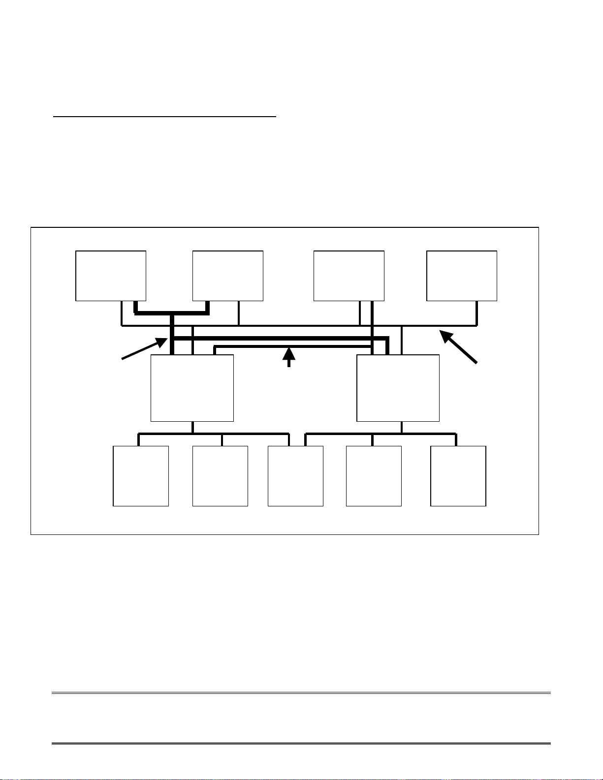
ADSP-2192 Architecture and Memory Map
The ADSP-2192 is a 16-bit DSP with dual 219x cores. The DSP architecture and memory map is shown in
Figures 1 and 2, respectively. For a detailed discussion, please refer the ADSP-2192 datasheet.
PCI 2.2
33MHz
32 Bit
USB 1.1
Serial
Interface
AC-97
Codec
Interface
GPIO
Eight Pins
PCI/USB
DMA
Bus
16K X 24
PM
RAM
219X
CORE
#1
160 MHz
64K X 16
DM
RAM
Figure 1. ADSP-2192 architecture
Serial
Codec
4K X 16
SHARED
RAM
CORE
160 MHz
32K X 16
DM
RAM
219X
#2
Periphera
l
Control
16K x 24
PM
RAM
EE-124 Page 2
Technical Notes on using Analog Devices’ DSP components and development tools
Phone: (800) ANALOG-D, FAX: (781)461-3010, EMAIL: dsp.support@analog.com, FTP: ftp.analog.com, WEB: www.analog.com/dsp
Page 3
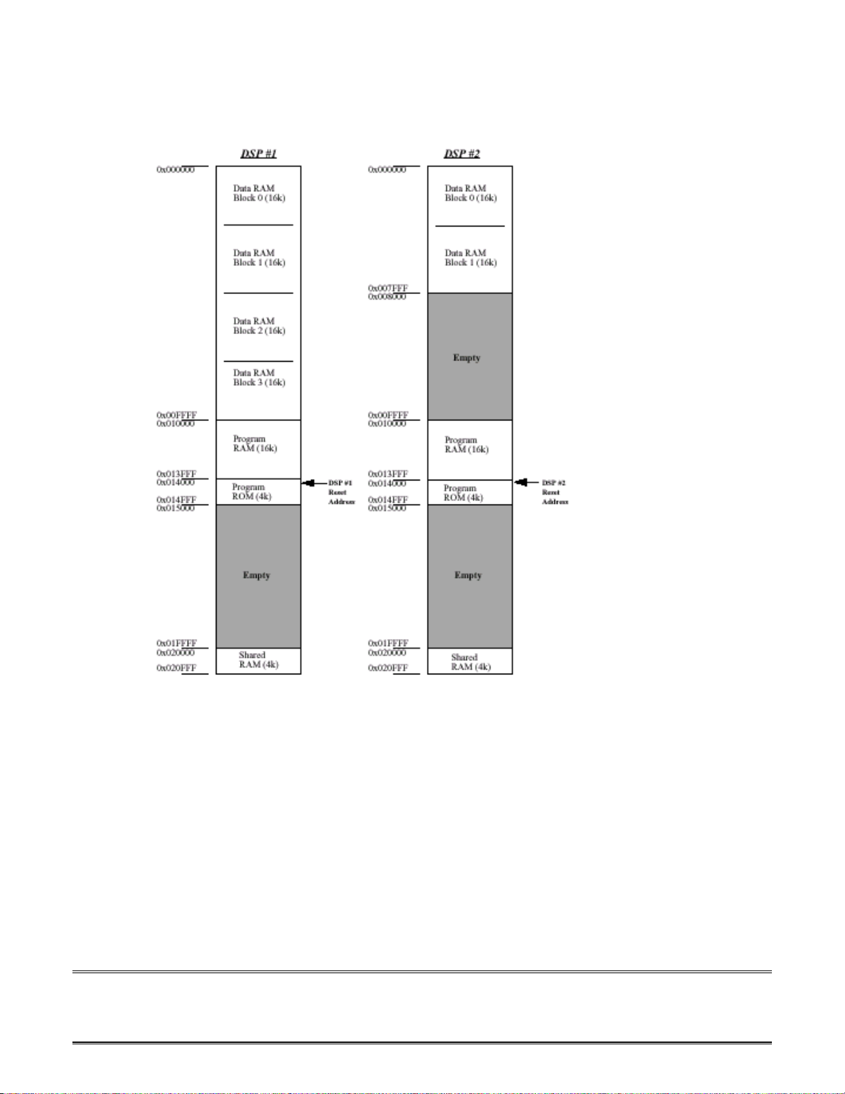
Figure 2. ADSP-2192 Memory Map
EE-124 Page 3
Technical Notes on using Analog Devices’ DSP components and development tools
Phone: (800) ANALOG-D, FAX: (781)461-3010, EMAIL: dsp.support@analog.com, FTP: ftp.analog.com, WEB: www.analog.com/dsp
Page 4
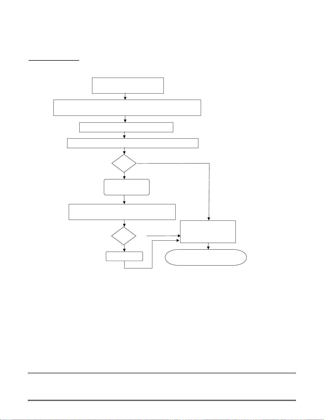
Booting Flowchart
Loader kernel reads CRST pins and determines Mode of
Booting; also performs housekeeping operations, setting up Interrupts, etc.
Loader Kernel reads BUS MODE pins to set up bus configuration
DSP emerges from ~RESET and
program flow jumps to Boot ROM
Call subroutine to auto-detect serial EEPROM
Serial EEPROM
Exists?
Yes
Determine 8 or 16-bit?
SPI or micro-wire?
Load serial EEPROM configuration and data
packets-load PCI/USB config registers accordingly
Do any serial EEPROM
need to be executed?
Yes
Execute Packets
No
Transfer Control to PCI
No
or USB to facilitate rest
of boot
After Booting is complete, user has
option to either return to serial EEPROM
or jump to user code and being execution
Finish
On emerging from RESET the loader kernel in DSP1’s ROM alone will attempt to read the serial EEPROM. The loader
kernel for DSP2 will not boot via the serial EEPROM. It will wait in a loop until DSP1 has completed reading data from the
serial EEPROM, at which point, both DSPs will booted directly via the PCI or USB interfaces.
EE-124 Page 4
Technical Notes on using Analog Devices’ DSP components and development tools
Phone: (800) ANALOG-D, FAX: (781)461-3010, EMAIL: dsp.support@analog.com, FTP: ftp.analog.com, WEB: www.analog.com/dsp
Page 5

Program Flow for the loader kernel
Upon recovering from RESET, the ADSP-2192 jumps to the first location of the Boot ROM at address
0x14000, which is the start of the loader kernel. The first task performed by the loader kernel is to
determine the type of RESET and the source of booting. This information is available by reading bits 8 and 9
(CRST<1:0>) of the Chip Mode/Status Register (CMSR) which determine the nature of DSP RESET.
CRST <1:0> RESET MODE
00 Power-on Reset
01 reserved
10 PCI/ISA/USB Hard Reset
11
Table 1. ADSP-2192 RESET modes
Soft Reset from CMSR RST Bit
Next, the loader kernel executes some housekeeping code, which consists of setting up and configuring
interrupts. It calls a routine which copies an interrupt table into the appropriate location in DSP RAM, with
only the TIMER interrupt enabled. The timer will be used if interfacing with a serial EEPROM.
Once the interrupt vector table and the corresponding registers have been configured, the loader kernel
determines whether a serial EEPROM is connected to the NVRAM interface. This is done by a call to a
subroutine that auto-detects a serial EEPROM. The detection routine verifies the existence of an external
EEPROM connected to the NVRAM interface of the chip. If a device does exist, parameters needed to
communicate with the device are loaded into scratch locations in data memory. Currently, the code will
detect 8-bit SPI EEPROMs that require either 8 or 16 bits of address, and 16-bit 3-wire Microwire
EEPROMs that require either 6 or 8 bits of address.
If it is determined that the reset source was a power-on reset, the BUSMODE pins of the chip are read to
determine whether boot is via PCI/USB/Sub-ISA or CardBUS interface. Accordingly, any default
configuration needed for the current bus mode is done in this routine. Most of the default configuration is
done by hardware containing appropriate default values on coming out of RESET. Any additional
configuration is done in software from the serial EEPROM.
Bits 10 and 11 of the CMSR Register (BUS<1:0>) determine the bus modes that the DSP comes up with.
These bits are only sensed at reset, and ignored thereafter.
EE-124 Page 5
Technical Notes on using Analog Devices’ DSP components and development tools
Phone: (800) ANALOG-D, FAX: (781)461-3010, EMAIL: dsp.support@analog.com, FTP: ftp.analog.com, WEB: www.analog.com/dsp
Page 6

Table 2. ADSP-2192 Bus Modes
Once the bus configurations have been configured (and if it was determined that a serial EEPROM exists),
the loader kernel calls a function to commence reading data from the serial EEPROM. Data format of serial
EEPROM boot-stream is described in the next section.
After the loader kernel has finished reading data from the serial EEPROM, it proceeds to set up and commit
bus configurations for the rest of booting via either the PCI or USB interfaces.
For example, for PCI this means that the configuration registers are set to be read-only and the part will
respond to PCI requests from the system host. For USB, the part will enter an idle loop and allow the
system host to detect and configure the part. (note: There is currently no configuration process required for
Sub-ISA mode.)
The final task performed by the loader kernel after bus configuration and transferring control to PCI or USB
is to enter an infinite loop, waiting for instructions. A pre-defined memory address - DM(0x000000) - is
regularly checked for commands. Once the PCI or USB device has completed booting the DSP, they can
write an instruction to this pre-defined location and have the DSP execute any one of a list of supported
commands. This include:
1. jump to program memory without returning. This instruction is used to leave the loader kernel and
begin user code
2. read word from EEPROM
3. enable write mode on EEPROM
4. write word to EEPROM
5. re-read patch block from EEPROM Used if bus configuration may have overwritten locations
6. enter power-down state
In addition to executing these commands while still in the loader kernel command loop, any piece of user
code during runtime may perform the above operations by writing the appropriate value into the pre-defined
memory address, and perform a CALL to address 0x014F00 (location in the ROM). This will cause the
loader kernel to perform the requested command and return control to the user code. Table 3 shows the
exact values and description of the various functions supported.
EE-124 Page 6
Technical Notes on using Analog Devices’ DSP components and development tools
Phone: (800) ANALOG-D, FAX: (781)461-3010, EMAIL: dsp.support@analog.com, FTP: ftp.analog.com, WEB: www.analog.com/dsp
Page 7

Value Description Argument 1 Argument 2 Argument 3
0x0000 nop N/A N/A N/A
0x0004 jump_to_code N/A dest. addr N/A
0x0006 eeprom_write_enable N/A N/A N/A
0x0002 eeprom_write_word eeprom addr source addr source page
0x0005 eeprom_write_imm_data eeprom addr imm. value N/A
0x0001 eeprom_read_word eeprom addr dest. addr dest. page
0x0003 read_patch_block eeprom addr N/A N/A
0x0007 powerdown dsp N/A N/A N/A
Table 3. Function values
In the case of a command requiring multiple arguments, the arguments are placed in DM(0x0001),
DM(0x0002), and DM(0x0003) respectively.
Boot-stream format
The serial EEPROM boot-stream format is shown in Figure 3. For the sake of simplifying the loader kernel,
the function that communicates with the serial EEPROM will present all received serial EEPROM data
(regardless of whether it comes from an 8-bit or 16-bit EEPROM) as 16-bit data to the loader kernel
software. While this eliminates the need to have separate sub-routines for 8-bit and 16-bit EEPROMs, this
will not have any effect on the external communication with the EEPROM itself.
Configuration Header
Format Identifier
Configuration Packet
Length
reserved
Configuration Header
Configuration Packet
Data Header
Data Packet
Format Identifier
Length
reserved
LS 16 bits of DSP destination addr
:
:
0xFFFF
Figure 3. Serial EEPROM boot-stream format
EE-124 Page 7
Technical Notes on using Analog Devices’ DSP components and development tools
Phone: (800) ANALOG-D, FAX: (781)461-3010, EMAIL: dsp.support@analog.com, FTP: ftp.analog.com, WEB: www.analog.com/dsp
Page 8

There are two types of packets that make up a boot-stream:
Configuration packets (or control packets)
These are packets which contain alternative configuration or register contents that will override the default
values;
Data can be contained within the external prom of the 2192 within several type of packets. Configuration
packets for each of the major bus modes (PCI, CardBus, USB, Sub-ISA) contain the information required to
initialize these interfaces. Inclusion of a configuration packet for any of these interfaces is optional; if no
packet is found, a default configuration will be used. Patch code packets can contain code that will be copied
into program memory of either DSP and optionally executed after PROM reading has been completed.
Any configuration packets on the PROM must be located at the low end of the addressable space, before any
patch code. If a configuration packet exists which matches the current bus mode (as determined by the
BUSMODE<1:0> pins of the chip), that packet will be processed and register values set accordingly.
Only one configuration packet for a given bus mode should exist in the PROM, though packets for non-active
interfaces are allowed (i.e., two PCI packets on the same PROM is disallowed, but a single PROM could hold
both a PCI packet and a USB packet).
Patch code should immediately follow the last configuration packet, or, if no configuration packets exist, it
should be in the first memory location. There can be any number of patch code packets that will write code
into any number of locations in program memory. It is required that all patch code for DSP1 precede any
patch code for DSP2. Only one block of patch code should have the execute flag set; after all PROM reading
has completed, the DSP will vector to the flagged code. If no code was flagged, the DSP will idle until woken
up by the host interface.
Header Format for Configuration Packets
All configuration packets will have a header in the following format:
Fomat Identifier address n
Length * n+1
Test Use n+2
Where “Length” is the number of 16-bit words in the packet, not including the header. The Test Use field
should be zero for all packets. The Format Identifier contains information about the type of configuration
information included in the packet.
Format Identifier
Individual bits within the “format identifier” word have the following functionality:
7 6:5 4 3 2 1::0
Type Busmode 16/8 unused unused PCI function
Bit 7 Type always 1 for configuration packets
EE-124 Page 8
Technical Notes on using Analog Devices’ DSP components and development tools
Phone: (800) ANALOG-D, FAX: (781)461-3010, EMAIL: dsp.support@analog.com, FTP: ftp.analog.com, WEB: www.analog.com/dsp
Page 9

Bits 6:5 Busmode 00 = PCI
01 = CardBus
10 = USB
11 = Sub-ISA
Bit 4 16vs8 1 if the PROM has 16-bit words
0 if the PROM has 8-bit words
Bits 3:2 unused These bits are reserved. They should be
written to 0.
Bits 1:0 PCI function # These bits are only defined for a PCI
configuration packet
00 if 1 function is enabled
01 if 2 functions are enabled
10 if 3 functions are enabled
11 invalid
Format of PCI Configuration Packets
PCI configuration packets are always of a fixed size and format, regardless of the number of PCI functions
enabled. There are 7 write-able registers in PCI configuration space for a given functions, and there are 3
possible functions, which means that each PCI config packet contains register values for a total of 21
registers. If one or more of the PCI functions is not in use, the values of the registers corresponding to that
function are don't cares, but they must be included in the PROM.
The seven config registers are listed within the packet in order or increasing address, so the order within the
packet is as follows:
1. Vendor ID
2. Device ID
3. Lower 8 bits = Rev ID
Upper 8 bits = 8 LSBs of Class Code
4. Upper 16 bits of Class Code
5. Subsystem Vendor ID
6. Subsystem Device ID
7. Power Management Capabilities Register
The complete PCI config packet will then be 24 (16-bit) words long, containing three words of header, then 3
sets of register values for PCI functions 0, 1, and 2, respectively. Since the Length field in the header refers
only to data words, this field will always be set to 21 for PCI config packets.
Note: ADI vendor ID = 0x11D4. ADI device IDs for ADSP-2192 are 0x2192, 0x219A, and 0x219E for PCI
function 0,1, and 2 respectively.
Format of USB Configuration Packets
EE-124 Page 9
Technical Notes on using Analog Devices’ DSP components and development tools
Phone: (800) ANALOG-D, FAX: (781)461-3010, EMAIL: dsp.support@analog.com, FTP: ftp.analog.com, WEB: www.analog.com/dsp
Page 10

USB configuration packets contain only the configuration header and five 16-bit register values. The rest of
the USB configuration is handled by the USB driver during the handshake process. The registers are listed
in the config packet in the following order:
1. Vendor ID
2. Product ID
3. Release Number
4. Attributes
5. Max Power
The complete USB packet should then be 8 (16-bit) words long, containing three words of header, then 5
words of data. The length field for all USB config packets should therefore be 5.
Patch packets (or data packets)
Patch packets contain code or data that will be copied into data, program, or shared memory as the packet is
processed. There can be any number of patch packets addressing any number of banks of memory in the
EEPROM. Optionally, a patch packet written into program memory can be given an EXECUTE flag. This
code will be executed in the form of a function CALL after all EEPROM packets have been processed, but
before the bus configuration is finalized. (note: any code executed this way must conclude with an RTS).
Header Format for Patch Packets
All patch packets will have a header in the following format:
Format Identifier address n
Length n+1
Test Use n+2
DSP Address n+3
Length and Test Use are defined in the same way as for the configuration packets. The DSP address field
refers to the lower 16 bits only; the upper 8 bits of address (the memory page) are encoded in the Format
Identifier. The Format Identifier contains information about the type of configuration information included
in the packet.
Format Identifier
Individual bits within the “Format Identifier word” for a data packet are defined below:
7 6:5 4 3 2 1 0
Type Mem Page 16/8 unused Execute unused unused
Bit 7 Type always 0 for patch code packets
Bits 6:5 Mem Page 00 = write to page 0 memory (data memory)
01 = write to page 1 memory (program memory)
10 = write to page 2 memory (shared memory)
11 = invalid
EE-124 Page 10
Technical Notes on using Analog Devices’ DSP components and development tools
Phone: (800) ANALOG-D, FAX: (781)461-3010, EMAIL: dsp.support@analog.com, FTP: ftp.analog.com, WEB: www.analog.com/dsp
Page 11

Bit 4 16vs8 0 if the PROM has 8-bit words
1 if the PROM has 16-bit words
Bit 3 unused This bit is reserved. It should be written to 0.
Bit 2 Execute 0 to copy data into memory without execution
1 to execute code before final configuration
Bits 1:0 unused These bits are reserved. They should be
written to 0.
No more than one patch header may have the execute flag set, and it must be a block written to page 1
program memory. If any code is tagged with this flag, it will be executed before the final configuration is
completed in PCI or USB mode.
The 16- or 24-bit data should be packed into the PROM as shown below. If the Mem Page field is set to
program memory, it is assumed that the data is packed as 24-bit wide data words, and will be written
accordingly. Otherwise, 16-bit data is assumed.
If 24-bit data is being packed, there must be an even number of 24-bit words
in the patch code. An extra 'nop' may be padded to the code if necessary.
8-bit vs 16-bit EEPROMs
All data fields are considered to be 16-bit fields, taking up a single word of 16-bit PROMs. In the case of SPI
EEPROMs, which are 8-bit devices, each field will take up two PROM locations.
All user accessible routines within the boot code refer to only 16-bit locations, therefore addressing SPI
devices in two word chunks.
Data formats in EEPROM
Data for the serial EEPROM will have the following format. Individual bits within a word are typically
shifted in or out starting with the most-significant bit.
16-bit data in 16-bit PROM
MSB1 LSB1
MSB2 LSB2
MSB3 LSB3
: :
EE-124 Page 11
Technical Notes on using Analog Devices’ DSP components and development tools
Phone: (800) ANALOG-D, FAX: (781)461-3010, EMAIL: dsp.support@analog.com, FTP: ftp.analog.com, WEB: www.analog.com/dsp
Page 12

16-bit data in 8-bit PROM
MSB1
LSB1
MSB2
LSB2
MSB3
LSB3
:
24-bit data in 16-bit PROM
MSB1 NSB1
LSB1 MSB2
NSB2#
LSB2
MSB3 NSB3
LSB3 MSB4
: :
24-bit data is 8-bit PROM
MSB1
NSB1
LSB1
MSB2
NSB2
LSB2
MSB3
NSB3
LSB3
:
The boot stream may contain any number of configuration packets, followed by any number of data packets.
However, it is required that all configuration packets must come before data packets.
Each packet contains a header that contains information about the starting destination address, type, and
size of the data comprising that packet.
Currently, configuration packets are defined for PCI/CardBus mode and USB mode.
The boot stream is terminated with the bit pattern 0xFFFF.
#
NSB stands for “next significant byte”
EE-124 Page 12
Technical Notes on using Analog Devices’ DSP components and development tools
Phone: (800) ANALOG-D, FAX: (781)461-3010, EMAIL: dsp.support@analog.com, FTP: ftp.analog.com, WEB: www.analog.com/dsp
 Loading...