

Page 1

a
a Engineer To Engineer Note
aa
EE-123
Technical Notes on using Analog Devices’ DSP components and development tools
Phone: (800) ANALOG-D, FAX: (781) 461-3010, EMAIL: dsp.support@analog.com, FTP: ftp.analog.com, WEB: www.analog.com/dsp
An Overview of the ADSP-219x Pipeline
Last modified 10/13/00
This tech-note is intended to provide a brief description of the salient features of the ADSP-219x pipeline to
users and programmers of the ADSP-219x, to help them to optimize their programs to maximize
performance and throughput. Specific cases that illustrate the pipeline operation (such as loops, jumps, and
interrupt calls) will be explained.
Knowledge of ADSP-2100 family assembly language (which is identical to ADSP-219x assembly) is assumed.
For more detailed information on the ADSP-219x pipeline, please refer the ADSP-219x User’s Manual.
Introduction
The ADSP-219x has a six-stage instruction pipeline comprising the Look-ahead, Pre-fetch, Fetch, Address
generation, Decode, and Execute stages. Note that as this is not an execution pipeline, the DSP core
executes every instruction in a single core cycle. A two-stage memory pipeline is incorporated within the
instruction pipeline. What this means is that it takes two core cycles for data to be available on the data bus
after the address has been placed on the address bus. Therefore, during any given cycle, up to 6 instructions
maybe in different stages of completion.
The additional depth in the pipeline allows a much increased operating speed for the processor core. The
functions of the different stages of the pipeline are briefly:
• Look-ahead. In the look-ahead stage, the pipeline places an instruction address on the PMA bus.
The look-ahead stage is also used by the sequencer in resolving bus conflicts. Since the two stages of the
pipeline that could possibly use the PMA bus are the look-ahead and the address generation, if there is a
conflict between these two stages on who acquires the bus, the sequencer looks in the instruction cache to
determine if the instruction that causes the conflict has already been cached. If it is determined that the
instruction was cached, the sequencer looks ahead for the instruction from the instruction cache, allowing
the address generation stage to use the PMA bus instead. If however, the instruction was not cached, the
address generation stage wins priority in the current cycle to use the PMA bus, while the program sequencer
will get the PMA bus in the next cycle.
• Pre-fetch. The pre-fetch stage is essentially spent waiting for memory accesses that were initiated in the
look-ahead stage.
• Fetch. In this stage, the instruction that was “looked-ahead” two cycles ago is fetched from program
memory, over the PMD bus.
Copyright 2000, Analog Devices, Inc. All rights reserved. Analog Devices assumes no responsibility for customer product design or the use or application of customers’ prod ucts or
for any infringements of patents or rights of others which may result from Analog Devices assistance. All trademarks and logos are property of their respective holders. Information
furnished by Analog Devices Applications and Development Tools Engineers is believed to be accurate and reliable, however no responsibility is as sumed by Analog Devices
regarding the technical accuracy of the content provided in all Analog Devices’ Engineer-to-Engineer Notes.
a
Page 2

• Address generation. In this stage, certain parts of the instruction are decoded, such as DAG operations. If
any memory data is required by the instruction, the address for this data is placed over the appropriate
address bus (PMA for PM data and DMA for DM data)
• Decode. This stage is used by the processor to decode the rest of the instruction and for setting up
computational units. It is also spent waiting for memory accesses to occur.
• Execute. In this stage, the instruction is executed, status conditions are set, and results and outputs
written to the appropriate destination.
Syntax and Terminology
For the remainder of the document, the following syntax will be followed in pipeline diagrams and
discussions. The stages of the pipeline will be indicated by their first letters in Boldface Upper-case,
addresses will be indicated by the prefix `a’ (e.g., a1,a2,a3..), while instructions will be prefixed by `i’ (e.g.,
i1,i2,i3..). The pipeline blocks will contain the corresponding instructions as they traverse through the
pipeline. Blocks that are crossed out ( ) represent instances where the sequencer has invalidated the
contents of that pipeline stage and effectively replaced that instruction with a NOP. Blocks grayed out (
) represent a cache-lookup.
Cache hit. A cache hit occurs when the program sequencer determines that the address for an instruction is
present in the instruction cache. The result of a cache hit is the sequencer gets the instruction from the cache
instead of fetching it from program memory, thereby freeing up the PMA bus for another access.
Cache miss. A cache miss occurs when the address looked up by the sequencer is not present in the
instruction cache. In the event of a cache-miss, the sequencer has to fetch the instruction from memory.
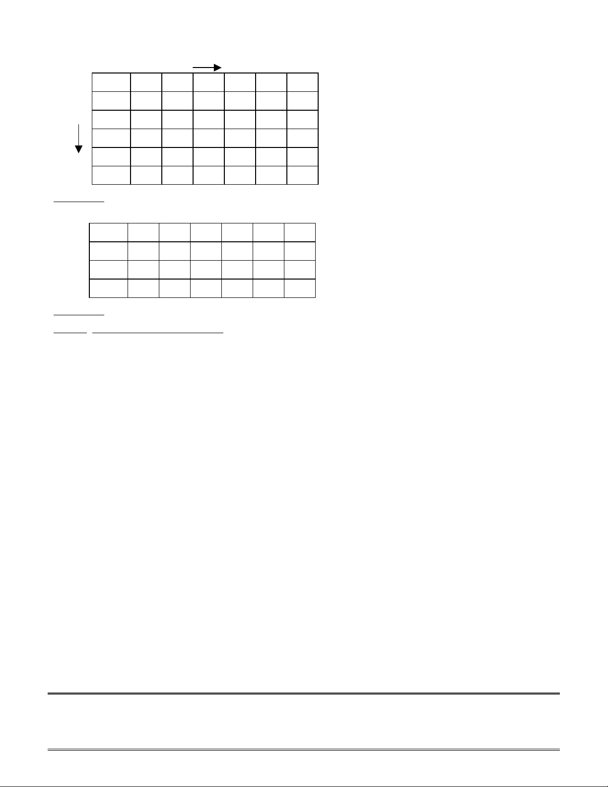
In relevant cases, the pipeline diagram will be accompanied with a block diagram describing the contents of
the Program Memory Address (PMA), Program Memory Data (PMD), Data Memory Address (DMA), and
Data Memory Data (DMD) buses in that cycle. For example, consider the following sequence of consecutive
instructions and addresses. Figure 1(a) shows the pipeline diagram, while Figure 1(b) shows the contents of
the four buses. (For the sake of simplicity, the contents of the DMA and DMD buses have been left out.)
Address Instruction
a1 i1
a2 i2
a3 i3
a4 i4
a5 i5
a6 i6
a7 i7
EN-123 Page 2
Notes on using Analog Devices’ DSP, audio, & video components from the Computer Products Division
Phone: (800) ANALOG-D or (781) 461-3881, FAX: (781) 461-3010, EMAIL: dsp.support@analog.com
Page 3
CLOCK CYCLES, TIME
PIPELINE
STAGE
L i6 i7 : : : :
P i5 i6 i7 : : :
F i4 i5 i6 i7 : :
A i3 i4 i5 i6 i7 :
D i2 i3 i4 i5 i6 i7
E i1 i2 i3 i4 i5 i6
Figure 1(a)
PMA a6 a7 a8 .. .. ..
PMD i4 i5 i6 .. .. ..
DMA
DMD
Figure 1(b)
Case 1
. Latencies on Jumps/Calls
In all, the ADSP-219x supports 5 varieties of delayed and non-delayed jumps and calls. There is a 13-bit
conditional jump/call (type 10), a 16-bit unconditional jump/call (type 10a), both of which use relative
addresses and not absolute addresses. The range of relative addresses (from the current PC) for the type 10
instruction is –4096 to +4095, while the corresponding range for the type 10a is –32768 to +32767.
In addition, the ADSP-219x also supports a delayed or non-delayed conditional Indirect Jump/Call (where
the address to jump or call is passed in a DAG index register). Note that the destination address is the
absolute address contained in the DAG register, with the 8 MSBs of the destination address taken from the
corresponding page register.
e.g., IF NE CALL (I4); // make sure you set up IJPG and I4 before you execute this instruction
IF AV JUMP (I5) (db); // same holds true for this instruction
Finally, the ADSP-219x also supports a 2-instruction, conditional, non-delayed absolute jump/call. The
absolute 24-bit address is specified in the instruction. The linker is cognizant enough when this jump is
invoked, to decide whether the absolute address needs to be specified. Whenever possible, the shorter, faster
relative jumps/calls will be used. There is a way to force the linker to use the absolute jump by prefixing the
jump with an “L”.
e.g., LJUMP foo;
LJUMP 0xFF0000;
The latency of the instruction pipeline is to introduce a latency of 4 “core processor” cycles for both
conditional as well as unconditional jumps and calls IF the branch is taken, and NO latency if the branch is
not taken. Figures 2(a) and 2(b) illustrate an example case of the branch taken, and branch not taken,
respectively.
EN-123 Page 3
Notes on using Analog Devices’ DSP, audio, & video components from the Computer Products Division
Phone: (800) ANALOG-D or (781) 461-3881, FAX: (781) 461-3010, EMAIL: dsp.support@analog.com
Page 4
Address Instruction
a1 i1: MR=MR+MX0*MY0 (SS);
a2 i2: IF COND JUMP aa1;
a3 i3
a4 i4
a5 i5
a6 i6
a7 i7
... ...
aa1 ii1
CLOCK CYCLES
L i6 ii1 ii2 : :
P i5 i6 ii1 ii2 : :
F i4 i5 i6 ii1 ii2 :
A i3 i4 i5 i6 ii1 ii2 :
D i2 i3 i4 i5 i6 ii1 ii2
E i1 i2 i3 i4 i5 i6 ii1
Figure 2(a) Branch taken
CLOCK CYCLES
L i6 i7 : : :
P i5 i6 i7 : : :
F i4 i5 i6 i7 : :
A i3
i4
i5 i6 i7 :
D i2 i3 i4 i5 i6 i7
E i1 i2 i3 i4 i5 i6
Figure 2(b) Branch not taken
Delayed Jumps/Calls
To compensate for the increased overhead, the ADSP-219x programming model now gives a programmer the
option (which didn’t exist on the ADSP-218x) to use delayed branches and function calls. Two instructions
can be executed in the pipeline pending the branch. Figure 3(a) and 3(b) shows the pipeline structure for a
delayed jump that is taken and not taken, respectively. Note that the instructions in the delayed branch
slots are executed regardless of whether the jump is taken or not. Also, there are some restrictions on the
types of instructions that can be part of a delayed branch slot. For example, stack manipulation operations
such as and pushes and pops of stacks are not allowed. Multi-word instructions are allowed only in the first
delay slot.
EN-123 Page 4
Notes on using Analog Devices’ DSP, audio, & video components from the Computer Products Division
Phone: (800) ANALOG-D or (781) 461-3881, FAX: (781) 461-3010, EMAIL: dsp.support@analog.com
Page 5

Address Instruction
a1 i1: MR=MR+MX0*MY0 (SS);
a2
a3 i3
a4 i4
a5 i5
a6 i6
a7 i7
... ...
aa1 ii1
CLOCK CYCLES
i2: IF COND JUMP aa1 (db);
L i6 ii1 ii2 : :
P i5 i6 ii1 ii2 : :
F i4 i5 i6 ii1 ii2 :
A i3 i4 i5 i6 ii1 ii2 :
D i2 i3 i4 i5 i6 ii1 ii2
E i1 i2 i3 i4 i5 i6 ii1
Figure 3(a) Branch taken
CLOCK CYCLES
L i6 i7 : : :
P i5 i6 i7 : : :
F i4 i5 i6 i7 : :
A i3
i4
i5 i6 i7 :
D i2 i3 i4 i5 i6 i7
E i1 i2 i3 i4 i5 i6
Figure 3(b) Branch not taken
Case 2. Pipeline Latencies on Interrupts and RTI/RTS
There is a minimum pipeline latency of 4-cycles in servicing an interrupt (Fig 4). This is in addition to cycles
taken for recognizing and synchronizing the interrupt. Additional delays maybe caused by DMA operations
occurring in the background, or the execution of I/O instructions. On receiving and recognizing an interrupt
request, the DSP completes execution of the present instruction, and in the very next cycle flushes the
pipeline while simultaneously looking up the first instruction of the interrupt vector (i_int1). There is also a
4-cycle hit on a return from an interrupt or from a function call.
EN-123 Page 5
Notes on using Analog Devices’ DSP, audio, & video components from the Computer Products Division
Phone: (800) ANALOG-D or (781) 461-3881, FAX: (781) 461-3010, EMAIL: dsp.support@analog.com
Page 6

Address Instruction
a1 i1
a2 i2
a3 i3
a4 i4
a5 i5
a6 i6
a7 i7
... ...
a_int1 i_int1
a_int2 i_int2
... ...
a_intz i_intz: RTI;
Interrupt is processed in this cycle
CLOCK CYCLES
L i6 i_int1 : : : : i3 i4 :
P i5 i6 i_int1 : : : :
i3
i4 :
F i4 i5 i6 i_int1 : : : : i3 i4 :
A i3 i4 i5 i6 i_int1 : : : : i3 i4 :
D i2 i3 i4 i5 i6 i_int1 : : : : i3 i4
E i1 i2 i3 i4 i5 i6 i_int1 : i_intz : : : : i3
First instruction of First instruction RTI
interrupt vector is of ISR is executed
loaded into top of pipeline
Figure 4
Delayed RTI/RTS
The delayed RTI or RTS can be used to reduce by half the number of wasted cycles in returning from a
serviced interrupt. Fig 5 describes the pipeline structure for this case. The number of non-productive cycles
is reduced from 4 to 2 with the use of a delayed return. There are some restrictions on the types of
instructions that can be part of the delay slots.
Address
a_int1 i_int1
a_int2 i_int2
... ...
a_intx i_intx: RTI (db);
a_inty i_inty
a_intz i_intz
Instruction
EN-123 Page 6
Notes on using Analog Devices’ DSP, audio, & video components from the Computer Products Division
Phone: (800) ANALOG-D or (781) 461-3881, FAX: (781) 461-3010, EMAIL: dsp.support@analog.com
Page 7

CLOCK CYCLES
L i6 i_int1 : : : : i3 i4 : :
P i5 i6 i_int1 : : : :
i3
i4 : :
F i4 i5 i6 i_int1 : : : : i3 i4 : :
A i3 i4 i5 i6 i_int1 : : i_intz : : i3 i4 :
D i2 i3 i4 i5 i6 i_int1 : : i_inty i_intz : : i3 i4
E i1 i2 i3 i4 i5 i6 i_int1 : i_intx i_inty i_intz : : i3
First instruction of First instruction RTI (db)
interrupt vector is of ISR is executed
looked up
Figure 5
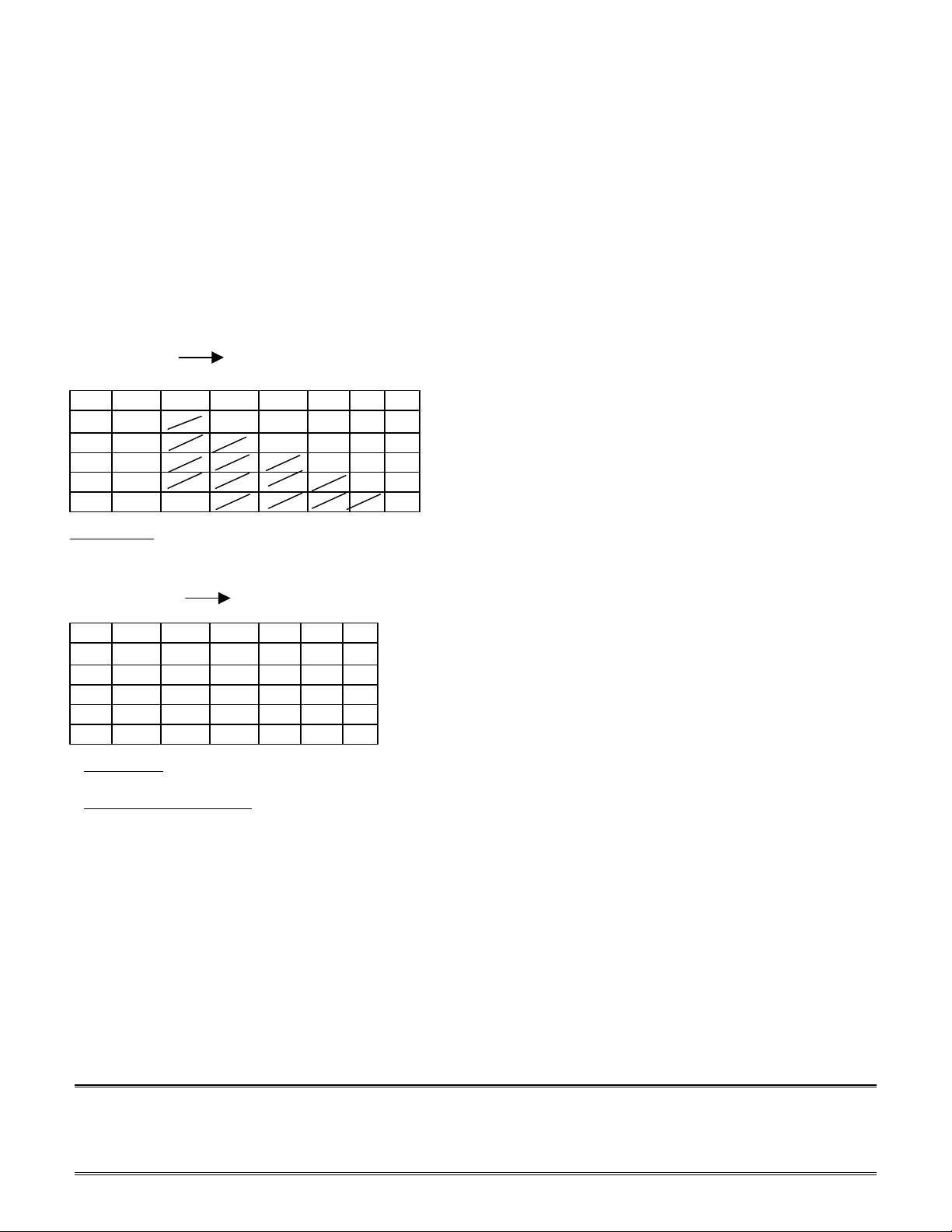
Case 3.
Do-Until Loops
Short Do-until loops offer an interesting case for the pipeline in terms of the number of iterations of a loop,
as well as the type of instructions that occur within the loop. In general, such loops incur a one-time
overhead of 4 cycles during loop entry. For example, consider a single-instruction loop that is executed 4
times. (For now, it is assumed that the instruction i5 in the loop is not a Type 1 instruction, i.e.,
Multifunction ALU or MACC with DM and PM dual reads using DAGs 1 and 2 post-modify -- this case will
be discussed later.)
Address Instruction
a1 i1
a2 i2
a3 i3: CNTR = 4;
a4 i4: DO this_loop UNTIL CE;
this_loop: a5 i5: (not a Type 1 ins)
a6 i6
a7 i7
a8 i8
... ...
CLOCK CYCLES
L i6 i7 i8 i5
P i5
F i4 i5
A i3 i4 i5
i6
0
i7
i6 i7 i8 i5
0
i8 i5
i6 i7 i8 i5
0
D i2 i3 i4 i5
E i1 i2 i3 i4 i5
i5
0
i6 i7 i8 i5
0
i5
1
0
0
1
i5
1
0
i6 i7 i8 i5
i5
i5
i5
i6 :
2
i5
1
i5
1
i5
0
i6
3
i5
2
1
0
i5
i5
3
2
1
0
:
i6
i5
i5
i5
3
2
1
i6 :
i5
3
i5
i5
2
i6 :
i6
3
Figure 6
EN-123 Page 7
Notes on using Analog Devices’ DSP, audio, & video components from the Computer Products Division
Phone: (800) ANALOG-D or (781) 461-3881, FAX: (781) 461-3010, EMAIL: dsp.support@analog.com
Page 8

Case 3. Long DO-UNTIL Loops
Do-until loops that are longer than 5 instructions deep have no overhead as illustrated in Figure 7.
Address Instruction
a1 i1
a2 i2
a3 i3: CNTR = 2;
a4 i4: DO this_loop UNTIL CE;
a5 i5 (not a Type 1 ins)
a6 i6 (not a Type 1 ins)
a7 i7 (not a Type 1 ins)
a8 i8 (not a Type 1 ins)
this_loop: a9
a10 i10
CLOCK CYCLES
L
i6
P
i5
F
i4 i5
A
i3 i4 i5
D
i2 i3 i4 i5
E
i1 i2 i3 i4 i5
i7
0
i6
0
i9 (not a Type 1 ins)
i8
0
0
0
i7
i6
0
0
0
0
i9
i8
i7
i6
i5
0
i9
0
i8
0
i7
0
i6
0
i6
1
i5
0
i9
0
i8
0
i7
0
i6
0
i7
1
i6
1
i5
0
i9
0
i8
0
i7
0
i8
1
i7
1
i6
1
i5
0
i9
0
i8
0
i9
1
i8
1
i7
1
i6
1
i5
0
i9
0
1
1
1
1
1
0
i10 :
i9
i8
i7
i6
i5
i10
1
1
1
1
1
i9
i8
i7
i6
1
1
1
1
:
i10 :
i9
i8
i7
i10
1
1
1
i9
i8
1
1
Figure 7
Case 4.
Type-1 Instructions
Type-1 instructions are one of the most powerful and commonly used DSP instructions and are widely used
in FIR and IIR tap implementations. Type-1 instructions encompass an ALU/MAC/Shifter operation
executed in parallel with dual-memory fetches. For a more detailed description of Type-1 instructions, please
refer the User’s manual. Type-1 instructions provide an interesting case because they require the use of
three buses, and on an architecture such as the 219x, this is accomplished using the instruction cache.
Figures 8(a) and 8(b) show the two cases to describe the two cases of what happens when a Type-1
instruction has already been cached (resulting in a cache-hit), and the case where it hasn’t been cached
(resulting in a cache-miss). Note that for a Type-1 instruction to execute in a single cycle, the instruction
should have been cached, and the two data operands should be placed in separate memory blocks.
EN-123 Page 8
Notes on using Analog Devices’ DSP, audio, & video components from the Computer Products Division
Phone: (800) ANALOG-D or (781) 461-3881, FAX: (781) 461-3010, EMAIL: dsp.support@analog.com
Page 9

CLOCK CYCLES
Cache-lookup and cache-hit
L i6 i7 i8 i9 :
P i5 i6
i7 i8 i9
F i4 i5 i6 i7 i8 i9
A i3 i4 i5 i6 i7 i8
D i2 i3 i4 i5 i6 i7
E i1 i2 i3 i4 i5 i6
123456
PMA
PMD
DMA
DMD
a6 a7
i4 i5 i6 i7
address
for i5’s
PM data
address
for i5’s
DM data
a9 : :
PM data
for i5
DM data
for i5
:
:
i9
Figure 8(a)
EN-123 Page 9
Notes on using Analog Devices’ DSP, audio, & video components from the Computer Products Division
Phone: (800) ANALOG-D or (781) 461-3881, FAX: (781) 461-3010, EMAIL: dsp.support@analog.com
Page 10

CLOCK CYCLES
L i6 i7 i8 i8 i9
P i5 i6
F
A
i4 i5 i6 i7
i3 i4 i5 i6
cache-miss
i7 i8
i7
adv
i6
adv
::
i9 :
i8 i9
i7 i8
D i2 i3 i4 i5 i6 i7
E i1 i2 i3 i4 i5 i6
1234567
PMA
PMD
DMA
DMD
a6 a7
i4 i5 i6 i7
address
for i5’s
PM data
address
for i5’s
DM data
a8 a9 :
PM data
for i5
DM data
for i5
i8 i9
Figure 8(b)
Case 4.
Do-Until Loops containing Type-1 Instructions
The operation and effects of the instruction pipeline become more interesting if the instruction within a DOUNTIL loop is a Type1 instruction, as shown in the following example for an FIR filter tap.
:
DO sop UNTIL CE;
sop: MR = MR+MX0*MY0 (SS), MX0 = DM(I0,M1), MY0 = PM(I4,M5);
:
In this case, since the instruction also uses the PMA and PMD buses, the instruction cache comes into the
picture, and there are pipeline conflicts that lead to added cycles. There are also varying latencies depending
on the number of iterations of the loop.
Generally, the number of cycles taken to execute a Type-1 Do-Until loop N times is (N+8) cycles. This
assumes the dual data operands have been placed in separate memory blocks.
EN-123 Page 10
Notes on using Analog Devices’ DSP, audio, & video components from the Computer Products Division
Phone: (800) ANALOG-D or (781) 461-3881, FAX: (781) 461-3010, EMAIL: dsp.support@analog.com
Page 11

Pipeline Stalls
Under certain conditions, stalls are automatically inserted in the pipeline by the sequencer. A stall causes
the entire pipeline to not advance. Stalls are completely transparent to the user and will not affect the
operation of user programs. There are two main reasons for stalls to be inserted in the pipeline.
The first is to enable background DMA transfers to occur. The other reason for stalls is if the code sequence
has dependencies. For example, consider the case below where DAG register I0 is initialized with a certain
value and is used for a memory access in the very next cycle. Since the DAG is not updated until the
instruction is executed, and since the DAG needs the updated value of I0 to perform the memory access, the
subsequent instruction cannot happen. Hence the sequencer stalls the pipeline for two cycles.
Address Instruction
a1 i1
a2 i2
a3 i3: I0 = 0x2;
a4 i4: ar = DM(I0,M1);
a5 i5
a6 i6
a7 i7
a8 i8
... ...
CLOCK CYCLES
L i6 i7
(stall)
P i5 i6
(stall)
F i4 i5
(stall)
A i3
i4
(stall)
i7
(stall)
i6
(stall)
i5
(stall)
i4
(stall)
i7 :
i6 : :
i5 i6 :
i4 i5 i6
D i2 i3 nop nop i4 i5
E i1 i2 i3 nop nop i4
Figure 9
EN-123 Page 11
Notes on using Analog Devices’ DSP, audio, & video components from the Computer Products Division
Phone: (800) ANALOG-D or (781) 461-3881, FAX: (781) 461-3010, EMAIL: dsp.support@analog.com
Page 12

The workaround (Fig 10) is to make sure these instructions are at least two apart.
Address Instruction
a1 i1: i0 = 0x2;
a2 i2
a3 i3
a4 i4: ar = DM(i0,m1);
a5 i5
a6 i6
a7 i7
a8 i8
... ...
CLOCK CYCLES
L
i6 i7 : : :
P i5 i6 i7 : : :
F i4 i5 i6 i7 : :
A i3 i4
i5 i6 i7 :
D i2 i3 i4 i5 i6 i7
E i1 i2 i3 i4 i5 i6
Figure 10
Conclusion
In conclusion, knowledge of the ADSP-219x instruction pipeline should allow users to write code to take
advantage of the increased speed and performance of the ADSP-219x architecture.
EN-123 Page 12
Notes on using Analog Devices’ DSP, audio, & video components from the Computer Products Division
Phone: (800) ANALOG-D or (781) 461-3881, FAX: (781) 461-3010, EMAIL: dsp.support@analog.com
 Loading...