

AN-655
MICROCONVERTER
ADuC832
AUTO-ZERO
OP AMP
AD8628
AUTO-ZERO
OP AMP
AD8628
TEC
CONTROLLER
ADN8830
WAVELENGTH
MONITOR PD
TEC
THERMISTOR
8
TUNABLE LASER
CW LASER
AVERAGE POWER
CONTROLLER
ADN2830
POWER
MONITOR PD
ETALON
FILTER
2.5V
REFERENCE
ADR291
12-BIT
DAC
12-BIT
DAC
12-BIT
SER ADC
T/H
MUX
GPIO
i8051
CW
LASER
AD8565
APPLICATION NOTE
One Technology Way • P.O. Box 9106 • Norwood, MA 02062-9106 • Tel: 781/329-4700 • Fax: 781/326-8703 • www.analog.com
Tunable Laser Reference Design for Designers with
the ADuC832/ADN8830/ADN2830
by Nobuhiro Matsuzoe
FEATURES
Single Board Solution for Tunable Lasers
8-Channel Selectable Wavelength Control
Wavelength Locking at 25 GHz/50 GHz Spacing
AutoPower Control (APC)
AutoTemperature Control (ATC)
AutoFrequency Control (AFC)
Laser Bias, Temperature Monitoring
EEPROM-Based Autorestoring
Serial Interfaces (SPI®/I2C®/RS-232) to Host System
Wavelength Stability < 2 pm (typ)
LD Temperature Stability < 0.01°C
APPLICATIONS
DWDM Transmission System
Optical Instrumentation
GENERAL DESCRIPTION
This tunable laser reference design offers a single board
solution with complete control requirements for DFB tunable laser subsystems. Designed to work from +3 V/–5 V
power supplies, it provides a low cost, low power tunable
laser solution designed for ease of use with standard
serial control interfaces.
A mixed-signal monolithic microprocessor, the ADuC832based wave locker feedback loop is designed to meet
the requirements of ITU-T grid spacing in a 50 GHz/25 GHz
system. An integrated 12-bit ADC with an 8- channel
multiplexer allows users to monitor laser bias current
and laser temperature via SPI, I2C, or RS -232C serial
interfaces. The ADN2830 laser bias controller can sink
up to 200 mA (single)/400 mA (dual) and its integrated
feedback control loop can maintain output optical power
constant over temperature changes during wave locking. The ADN8830 TEC controller enables excellent laser
temperature stability and precise wavelength control
with 1 pm resolution. A patented PWM/linear based TEC
drive architecture enables high efciency and minimizes
external ltering components.
REV. B
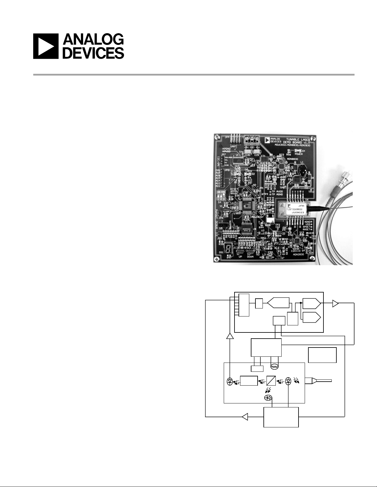
FUNCTIONAL BLOCK DIAGRAM
AN-655
–3–
AN-655
∆f F B
where:
F is the frequency slot
B is the bit rate.
S
S
<
(
)
– . /2 0 4
THERMISTOR TEC
WAVE
LOCKER
POWER
MONITOR
LASER
DIODE
MODULATOR
TEC CONTROLLER
ADN8830
I/V
AD8628
LASER CONTROLLER
ADN2830
ANALOG I/O
MICROPROCESSOR
DIGITAL I/O
SERIAL PORT
MICROCONVERTER ADuC832
I2C LINK TO HOST
2
CONTINUOUS
OPTICAL OUT
MODULATED
OPTICAL OUT
TRANSMIT DATA
2
TURNABLE LASER MODULE
REV. B
Figure 1. Typical Block Diagram of Optical
Transmitter with DFB Laser Module
WAVELENGTH TUNING
Because an optical transmitter requires a small formfactor design, use of the refractive index of a semiconductor laser is commonly used to alter the wavelength. As the
refractive index can be changed by both the temperature
and the density of carriers, transmitter designers can choose
from two different types of the wavelength-tunable laser
modules—distributed feedback (DFB) lasers and distributed Bragg reector (DBR) lasers. In general, the DBR
laser is capable of a fast tuning speed and a wide tuning
range. However, it requires multiple programmable current sources for wavelength control, which results in a
complex system design. In contrast, the DFB lasers can be
controlled by temperature of the laser chip, which results
in a lower system cost and higher reliability since the DFB
lasers are widely used today. The wavelength of the DFB
laser is related to temperature with a typical temperature
coefcient of 0.1 nm/K. By using a thermoelectric cooler
(TEC) and a thermistor with a built-in module, the laser
chip temperature can be adjusted, thus wavelength is
controlled. Figure 1 shows a simplied block diagram of
an optical transmitter designed with the DFB laser. The
wavelength tuning range of the DFB laser is limited by an
allowable operating temperature range. In fact, DFB lasers
provide a tuning range of a couple of nanometers which
is equivalent to 8 to 16 ITU-T grid channels depending on
the channel-to-channel spacing of the wavelength.
WAVELENGTH LOCKING
The internal or external wavelength locker generates
two monitor signals corresponding to the wavelength
and optical output power respectively. The wavelength
locker consists of the wavelength selective element and
the photodetector diode as shown in Figure 2a. The builtin Fabry Perot etalon works as a wavelength lter which
has a periodic characteristic similar to a comb lter. The
peak-to-peak range of the etalon lter, referred to as the
Free Spectral Range (FSR) cycle FS, is precalibrated by the
manufacturer to align with the ITU grid spacing as shown
in Figure 2b. Because the monitor signal has periodic
cycles, the algorithm of wavelength locking requires two
different tuning methods, coarse tuning, and ne tuning.
During the rst phase, the laser temperature must settle
to the particular temperature corresponding to the target
wavelength, where the wavelength is assumed within
the capture range. In the case of Figure 2b, there are two
locking points on both slopes, positive slope and negative
slope, within a single FSR. Thus, the capture range must
be half of the SFR. Feedforward control with a look-up
table is used in this coarse tuning phase. After the wavelength settles within the capture range, the ne tuning
phase acquires the wave length errors between the target
wavelength and actual wavelength by monitoring the wave
locker signal. Then the wavelength errors will be fed back
to the temperature control circuit. The ne tuning phase
maintains the wavelength within an allowable wavelength
deviation range over ambient temperature changes. The
ITU-T recommendation species wavelength stability as
a frequency deviation in G.692. This deviation is dened
as the difference between the nominal central frequency
and the actual central frequency (Figure 2c). A maximum
frequency deviation is given by
In 10 Gbps transmit applications with 50 GHz Grid spacing, the frequency deviation f must be less than 7.5 GHz
which means wavelength deviation
67 pm. The test result of the wavelength deviation taken
must be less than
by the reference design is shown in Figure 2d.
–2–
REV. B
ETALON
FILTER
I/V
I/V
OPTICAL
INPUT
POWER
MPD
WA
VELENGTH MPD
WAVELENGTH LOCKER
OPTICAL
OUTPUT
TO
µC
TO
µC
Figure 2a. Wavelength Locker Block Diagram
WAVELENGTH
MONITOR PD
LOCK POINT
WAVELENGTH (nm
)
MONITOR CURRENT (A)
POWER
MONITOR PD
FSR
F
S
TUNABLE RANGE = 3nm
F
OPTICAL POWER (dB)
WAVELENGTH (THz)
NOTES
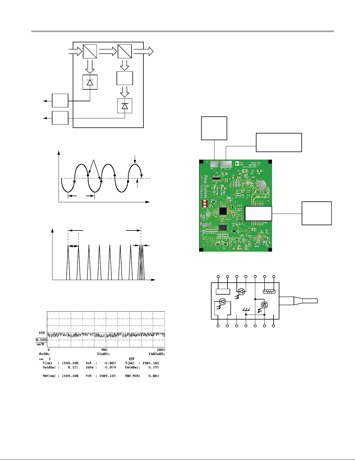
1. 1-HOUR WAVELENGTH STABILITY AT 25C, WAVE LOCKER ENABLED,
2 SEC INTERVAL.
2. F: LOCK POINT 1.5pm MAX TO MIN: 3pm.
3. LASER: FLD5F15CA, FUJITSU QUANTUM DEVICES LTD.
4. THE WAVELENGTH STABILITY IS MEASURED IN 3pm ACCURACY.
5. AFC STABILITY IS AFFECTED BY ACCUMULATIVE ERRORS OF APC AND
ATC CONTROL LOOP.
RS-232C
CABLE
FC-APC
(PANDA FIBER)
LASER
MODULE
COMPUTER
POWER SUPPLY
(+5V/–5V)
WAVELENGTH
METER
R
TH
PD1
PD2
7
6
5 4 3 2
1
8 9
10 11 12 13 14
TEC
AN-655
DEMONSTRATION BOARD
The tunable laser reference design board (demo board)
demonstrates autopower control (APC), autotemperature
control (ATC) and autofrequency control (AFC). Figure 3
shows simplied setup of the demo board. The demo board
has a mount space for a tunable DFB laser module in a 14-lead
buttery package. The demo board also provides a power
supply terminal, analog I/O ports, and a serial port. To mount
laser modules, a power photodetector must be oating within
the laser module package as seen in Figure 4.
Figure 2b. Wavelength Locker Characteristics
Figure 2c. Frequency Slots and Allowable
Frequency Deviation
Figure 3. Demo Board Setup
Figure 4. Laser Module Pin Assignment (reference: Fujitsu Quantum Devices, FLD5F6CA Data
Sheet)
REV. B
Figure 2d. AFC Typical Performance
–3–
AN-655
–5–
AN-655
V V R I V
where:
V V
R
LOCKPOINT REF m
REF
= ×
(
)
[ ]
=
[ ]
=
[ ]
–
.
46 2
46
2 50
2490 Ω
V G T V V
where:
T is target temperature of the thermistor in Celsius.
G =
V V
DAC LASER OFFSET
LASER
OFFSET
= ×
(
)
[ ]
=
[ ]
–
.
– .
0 0658
0 659
REV. B
GETTING STARTED
To ensure proper operation, follow the steps below.
1) Calculate the target voltages of the wavelength lock point according to the following equation:
The photo current Im2 needs to be solved at each lock point, because the Im2 may differ from lock point to lock point, laser
to laser. Table 1 is an example of the calculation result from the 8-channel wavelength tunable laser module.
Table 1.
Wavelength Im2 V
[nm] [THz] [mA] [V] [Dec] [Hex]
0 1582.439 189.4496 521.4 1.202 1969 07B1
1 1582.851 189.4003 573.4 1.072 1757 06DD
2 1583.265 189.3508 511.4 1.227 2010 07DA
3 1583.692 189.2997 563.4 1.097 1798 0706
4 1584.110 189.2498 527.4 1.187 1944 0798
5 1584.529 189.1997 556.8 1.114 1824 0720
6 1584.942 189.1504 524.3 1.194 1957 07A5
7 1585.365 189.1000 553.3 1.122 1839 072F
LOCKPOINT
Lock Point ADC Code
2) Calculate the voltage setpoint for ADN8830 according to the following equation:
Table 2 is an example of the calculation result from the 8-channel wavelength tunable laser module.
Table 2.
Curve
Wavelength RTH T
[nm] [THz] [] [C] [V] [Dec] [Hex]
0 1582.439 189.4496 16810 12.191 0.144 236 00EC Positive
1 1582.851 189.4003 14370 15.941 0.390 639 027F Negative
2 1583.265 189.3508 12350 19.658 0.634 1040 0410 Positive
3 1583.692 189.2997 10630 23.433 0.883 1447 05A7 Negative
4 1584.110 189.2498 9220 27.106 1.125 1843 0733 Positive
5 1584.529 189.1997 8040 30.728 1.363 2233 08B9 Negative
6 1584.942 189.1504 7060 34.247 1.594 2612 0A34 Positive
7 1585.365 189.1000 6210 37.802 1.828 2996 0BB4 Negative
LASER
V
DAC Code Slope
DAC
–4–
REV. B

AN-655
Maximum TEC voltage V VLIM V= −
( )
×
[ ]
1 5 4.
3) Compile and download the software to the ADuC832. To select the download/debug mode, position the switch (S5) to
DEBUG, and then press the reset button (S3).This sets the ADuC832 to download mode. To select the normal mode, position the switch (S5) to NORMAL and press the reset button (S3). ADuC832 executes downloaded program after reset.
4) Mount the laser module to the mount pads labeled U13. The ADN2830 is capable of sinking a current up to 200 mA. The
maximum TEC voltage limit is set at 3.5 V ±5% by default. To change the TEC voltage limiter, change the value of R24 and
R25 which is congured as a voltage divider to set the voltage to the VLIM pin of ADN8830. Maximum TEC voltage can
be given by:
5) Set JP1 and JP2. To protect the laser module from accidental damage, it is recommended to close JP1 and JP2 if the
program has been changed. Shorting JP1 enables the ADN8830 to shut down mode regardless of control signals from
the ADuC832. Shorting JP2 enables the ADN2830 to ALS (Automatic Laser Shutdown) mode regard less of control signals
from ADuC832.
6) Apply +3 V and –5 V to the power supply terminal block (J1) located at the top of the demo board.
7) Leave JP2 open. ADN2830 starts to drive the laser diode.
8) Calibrate the optical output power by adjusting the multiturn potentiometer (R48).
9) Leave JP1 open. ADN8830 starts to control the laser temperature to the initial temperature setpoint selected by switch (S4).
10) Press S1 or S2 buttons to change the wavelength lock point. S1 increments and S2 decrements the wavelength point by 1.
11) To change the target wavelength lock point directly, congure the 3-bit DIP switch (S4) according to Table 3. This change
is effective only when the ADuC832 is powered up or after reset.
Table 3.
Ch# S4(1) S4(2) S4(3)
0 OFF OFF OFF
1 ON OFF OFF
2 OFF ON OFF
3 ON ON OFF
4 OFF OFF ON
5 ON OFF ON
6 OFF ON ON
7
12) 7-segment LED (DS1) displays the selected wavelength and DS1 blinks until the laser temperature is set. TEMPLOCK LED
(D1) is lit when the laser temperature is settled within the capture range. WL_LOCK LED (D2) is lit when the wavelength
is locked within ITU grid ±12pm.
ON ON ON
REV. B
–5–
AN-655
–7–
AN-655
V I V
im m2 2
2 5 2490= ×
(
)
[ ]
. –
NOT POPULATED
DAC1
2.5V REF
R57
0
R58
R46
249
I
m2
V
m2
A
VDO
DAC0
R1
TEMPSET
THERMIN
ADN8830
2.5V
ADuC832
R
TH
R3
R2
LINEARIZATION
ERROR < 0.5%
IDEAL
ACTUAL
2.5
0
CONTROL VOLTAGE (V)
THERMISTOR TEMPERATURE (C)
10 50
R = R exp B
1
T
–
1
T
where:
R
is thermistor resistance at 25 C.
B is thermistor constant
T
is temperature in K.
Typically, B = 3450 and R 10K
TH 25
x
25
25
25
25
×
°
=
R
R R
R R
R
R R
R R
R
R R R R – R R
R R
R
where:
R R R
R R
R
low high
low high
low high
low high
mid high mid low high low
high low mid
high high
low low
1
2
2
2
3
2
2
3
3
=
′ ′
′ ′
=
′ ′
′ +
′
=
+
+
′ =
+
′ =
+
–
–
REV. B
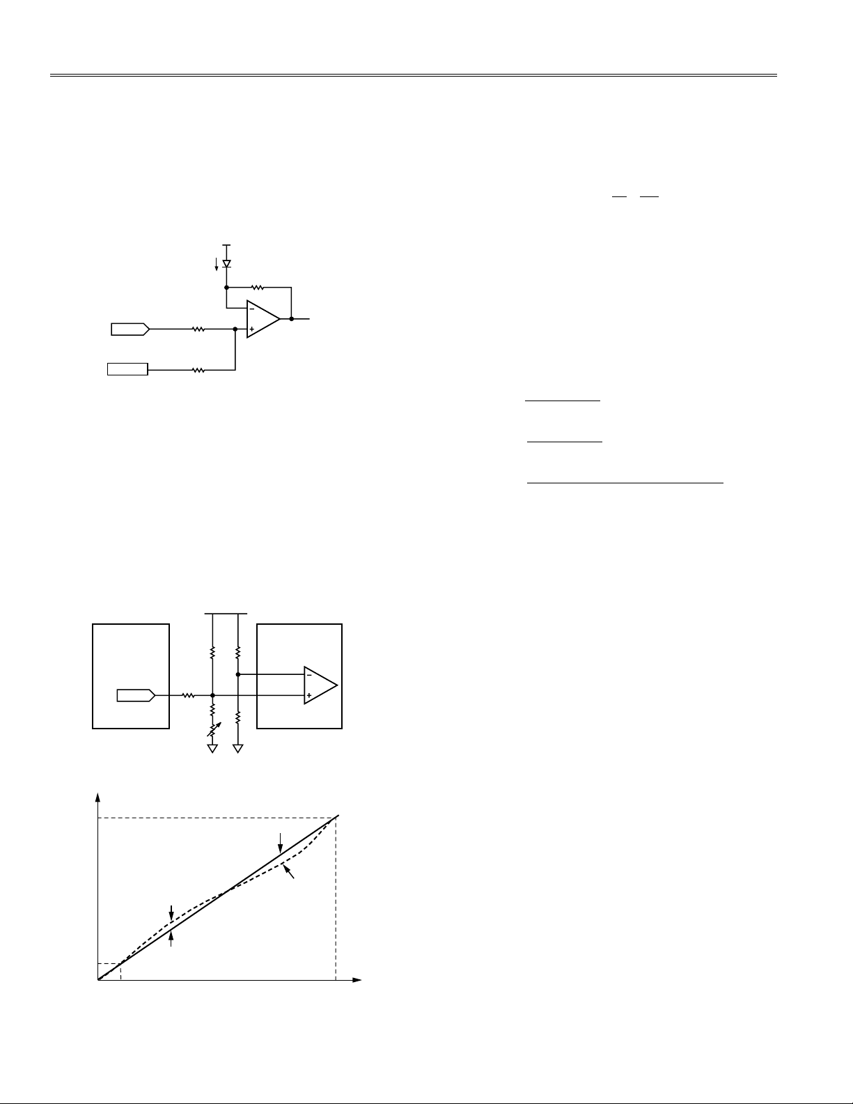
INTERFACING WAVELENGTH MONITOR PD
Figure 5 shows the current-to-voltage conversion circuit
on the demo board. The conversion gain is set by R46.
The input range of the wavelength monitor current Im2 is
up to 1.0 mA by default. The wavelength monitor voltage,
V
, is calculated by:
im2
Figure 5. I/V Conversion Circuit
INTERFACING 12-BIT DAC AND ADN8830
By using the interface circuit shown in Figure 6, the laser
temperature is controlled by DAC output voltage. This
scales the DAC voltage range from 0 V to 2.5 V for temperature range from 10°C to 50°C. The interface circuit
linearizes the thermistor transfer function. The TEMPSET
pin of ADN8830 is xed at 1.25 V. The THERMIN pin is
connected to the resistor network which includes the
thermistor. The characteristic of voltage-to-temperature
is shown in Figure 7.
Figure 6. Application Circuit Using DAC Control Voltage
Figure 7. V-to-Temperature Characteristic
To maintain optimal linearity over the required temperature
range, the value of the thermistor resistance should be
calculated at the lowest and the highest operating temperature according to the following equation:
R1, R2, and R3 are given by:
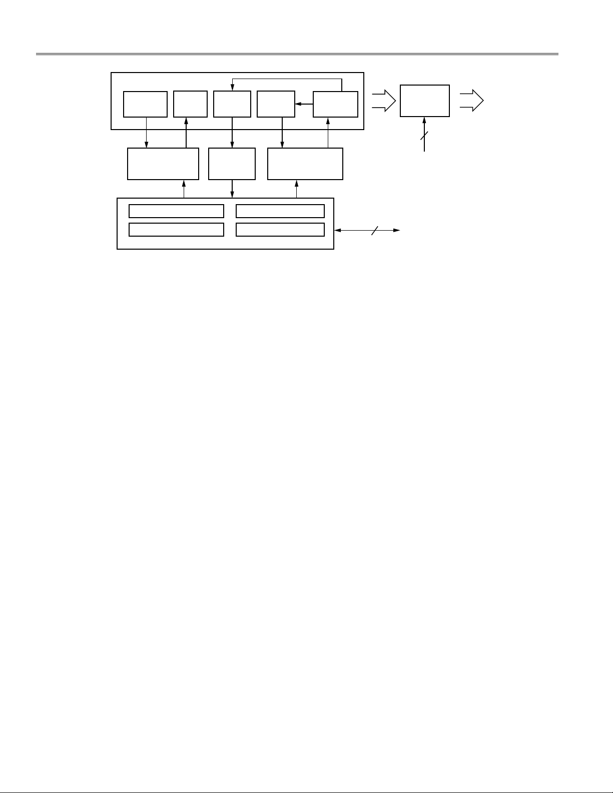
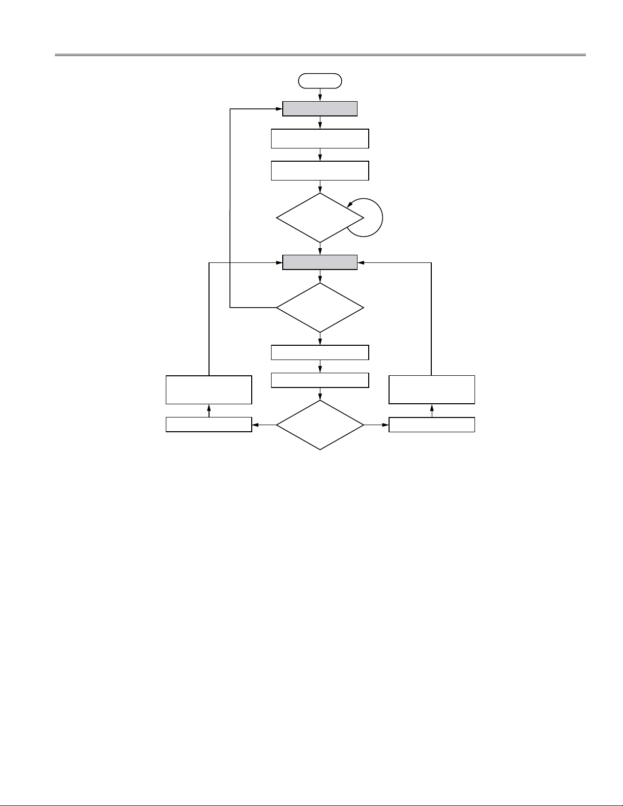
IMPLEMENTING THE WAVELENGTH LOCK
As the rst phase, the program executes the coarse tuning
with the ADN8830 TEC controller. The program reads S4
switch position, then generates the xed control voltage to
let the ADN8830 settle the laser temperature corresponding to the selected wavelength set by S4. Because the
ADN8830 has a local control loop for the temperature
control, the program waits for the temperature locked
signal from the ADN8830. After the laser temperature is
settled within the capture range of the wavelength lock,
the program starts the ne tuning. This phase uses the
monitor signal from the wavelength locker. The program
reads the actual wavelength and compares with the target
wavelength being stored in the memory. Then the program
adjusts the temperature control voltage, which corresponds
to the error amount between the target wavelength and
the monitored wavelength. Figure 8 shows the overview
of the program ow including the course and ne tuning.
Details of the course and ne tuning are shown in Figure 9
and Figure 10 respectively.
–6–
REV. B
AN-655
YES
NO
YES
NO
COMPARE
AC
QUIRED DATA WITH
TA
RGET DATA
TARGET CHANNEL
CHANGED?
START COARSE TUNE
MOVING AVERAGE FILTERING
START A/D CONVERSION
NEGATE LASER AND TEC
SHUTDOWN
LOAD AND SET AN INITIAL
TEMPERATURE
START FINE TUNE
START
SET LOOP GAIN
UPDATE D/A CONVERTER
TO
INCREMENT LASER
TEMP
SET LOOP GAIN
UPDATE D/A CONVERTER
TO
DECREMENT LASER
TEMP
LASER TEMP IN
CAPTURE RANGE OF
WA
VE LOCKER?
Figure 8. Overview of Program Flow Chart
REV. B
–7–

AN-655
–9–
AN-655
START COARSE TUNE
TEMPERATURE
LOCKED?
NO
TURN OFF
LASER/TEC
LOAD TARGET DATA
READ S4 SWITCH
ADC GAIN/OFFSET
CALIBRATION
LOCK POINT
CALIBRATION
SET LOCKING SLOPE
SET TARGET
TEMPERATURE
TURN ON
LASER/TEC
GO TO FINE TUNE
DELAY
REV. B
Figure 9. Coarse Tuning Flow Chart
–8–
REV. B

AN-655
START FINE TUNE
CHECK SLOPE
POLARITY
LP < ADC
FLAG = 0
GRID CHANNEL
CHANGED?
8 A/D
CONVERSIONS
AVR. FILTERING
LOCKPOINT–ADC
INCREMENT LASER
TEMPERATURE
DECREMENT LASER
TEMPERA
TURE
DELAY
ELSE
YES
POSITIVE SLOPE
BACK TO
COARSE TUNE
LP > ADC
FLAG = 1
GRID CHANNEL
CHANGED?
8 A/D
CONVERSIONS
AVR. FILTERING
LOCKPOINT–ADC
INCREMENT LASER
TEMPERATURE
DECREMENT LASER
TEMPERATURE
DELAY
ELSE
YES
NEGATIVE SLOPE
BACK TO
COARSE TUNE
NONO
Figure 10. Fine Tuning Flow Chart
ADuC832 SOFTWARE
The demo software is written in i8051 assembly that uses 1.2 kB out of 62 kB on-chip EE/Flash and 80 bytes out of 256 bytes
of on-chip RAM in ADuC832. The transaction time of the wavelength lock routine is approximately 0.3 ms at 4 MHz of the CPU
core clock setting. The essential part of the program is listed below. The rst control phase is labeled FF_Tune (Feed-Forward
Tuning), and second control phase is labeled L_Lock (Lambda Lock).
ORG 0060H ; MAIN PROGRAM
MAIN: ; ===cpu congure===
SETB ALS ; Shutdown laser driver, ADN2830 (ACTIVE HIGH)
CLR SD ; Shutdown TEC, ADN8830 (ACTIVE LOW)
MOV ADCCON1, #11001100b ; Select Ext. Vref, single conversion
MOV DACCON, #00011111b ; DAC0 On, 12bit, Asynchronous
MOV DAC0H, #007h ; DAC0 to 4th WL, Set TEMP =28.033degC
MOV DAC0L, #096h ;
MOV PLLCON, #00000000b ; Set core clock to 16MHz
SETB EA ; Enable Interrupt
MOV P0, #00101000b ; Turn on 7SEG display with ‘8’
CLR LLOCK_LED ; Turn off WL Lock LED
MOV CALN_L, #020h ; Lock point calib. value at neg. slope
MOV CALN_H, #000h ;
MOV CALP_L, #010h ; Lock point calib. value at pos. slope
MOV CALP_H, #000h ;
MOV CALDAC_L, #000h ; DAC initial value calib. low byte
MOV CALDAC_H, #000h ; DAC initial value calib. high byte
REV. B
–9–

AN-655
–11–
AN-655
REV. B
CALL DACDATA ; Load DAC data table to ram (30h to 3Fh)
CALL LP_DATA ; Load lock point data table to ram (40h to 4Fh)
CALL SW_DETECT ; Read 3-bit DIP SW position
CALL ADCCAL ; ADC Gain and Offset calib.
CALL AUTO_DEMO ; Enable Auto demo if S1/S2 pushed
MOV ECON, #06H ; Erase all pages of data Flash/EE
CALL REV_WRITE ; Write board and rm revision to Flash/EE
FF_TUNE: ; ===Feed-forward tuning (coarse-tune)===
SETB ALS ; Turn off Laser, Active High
CLR SD ; Turn off TEC, Active LOW
CLR PBFLAG ; Clear PBFLAG
CLR P3.6 ; Turn off Temp lock LED
CALL CH_LOAD ; Load selected DAC initial value
CALL LP_LOAD ; Load selected Lock point value
CALL SLOPE_CHECK ; Check slope polarity
MOV P0, WL_SEL ; display selected wavelength ch# on 7seg
SETB LEDBI ; Turn on 7seg display
SETB LEDLE ; 7seg Latch enabled
CALL LP_CAL ; Lock point offset calibration
CALL DAC_CAL ; DAC initial value calibration
MOV DAC0H, DACINT_H ; Update DAC to target temp
MOV DAC0L, DACINT_L ; Update DAC to target temp
SETB SD ; Turn on TEC
CLR ALS ; Turn on Laser
CLR TMPLKFLAG ; Clear temp lock indicate ag
MOV R0, #00H ; SET Page Pointer ADDRESS
MOV R1, #03H ; SET Byte Location ADDRESS
MOV R2, WL_SEL ; SET 1byte Value to write
CALL EE_WRITE ; Call Flash/EE Write routine
CALL TEMP_LOCK ; Sit here until FF_Tune completion
L_LOCK: ; ===Lambda lock Loop (ne tune)===
SETB LEDBI ; Turn on 7seg display
MOV A, #07h ; Set delay time, A*12.5msec
CALL DELAY ; Call delay program, 100msec
JNB SLOPEFLAG, LL_POS ; Check slope polarity, positive or negative
LL_NEG: ; ==Lambda locking at Negative slope==
CALL PB_DETECT ; Detect push-button sw
JNB PBFLAG, LOOP_N ; Jump LOOP_N if PB is not pushed
JMP FF_TUNE ; if PBFLAG=1(PB detected), back to FF_TUNE
LOOP_N:
MOV A, #40d ; Set delay time, A * 12.5msec
–10–
REV. B

CLR P2.7 ; Test signal for cpu transaction monitoring
CALL DELAY ; Call delay program
SETB P2.7 ; Test signal for cpu transaction monitoring
CALL ADC ; Take 8 * samples
CALL AVR ; Averaging
CALL SUBTRACT ; Subtract (LOCKPOINT - ADCDATA)
CALL LOCK_INDICATE ; Turn LED on if result is in lock range
CALL GAIN_DECISION ; Check if error amount is <2LSB, <16LSB
CALL ADJUST_N ; Call dac update routine
CALL LD_BIAS_MONITOR ; Monitor Laser Bias on ADC1
CALL LD_TEMP_MONITOR ; Convert DAC0H/L code to temperature value
CALL CPU_TEMP_MONITOR ; Monitor on-chip temp sensor
JMP LL_NEG ; Back to loop top
LL_POS: ; ==Lambda locking at Positive slope==
CALL PB_DETECT ; Detect push-button sw
JNB PBFLAG, LOOP_P ; Jump LOOP_P if PB is not pushed
JMP FF_TUNE ; if PBFLAG=1(PB detected), back to FF_TUNE
LOOP_P:
MOV A, #40d ; Set delay time, A * 12.5msec
CLR P2.7 ; Test signal for cpu transaction monitoring
CALL DELAY ; Call delay program
SETB P2.7 ; Test signal for cpu transaction monitoring
CALL ADC ; Take 8 * samples
CALL AVR ; Averaging
CALL SUBTRACT ; Subtract (LOCKPOINT - ADCDATA)
CALL LOCK_INDICATE ; Turn LED on if result is in lock range
CALL GAIN_DECISION ; Check if error amount is <2LSB, <16LSB
CALL ADJUST_P ; Call dac update routine
CALL LD_BIAS_MONITOR ; Monitor Laser Bias on ADC1
CALL LD_TEMP_MONITOR ; Convert DAC0H/L code to temperature value
CALL CPU_TEMP_MONITOR ; Monitor on-chip temp sensor
JMP LL_POS ; Back to loop top
; END OF MAIN PROGRAM
AN-655
REV. B
–11–

AN-655
–13–
AN-655
REV. B
SOFTWARE MEMORY MAP
Table 4. Internal RAM, Lower 128 Bytes
Byte Address Byte Name Byte Description
00 to 1F – Reserved
20 Control Flags Detailed in Bit Memory Map
21 WL_SEL Wavelength select
22 CALDAC_L Offset calibration for DAC
23 CALDAC_H
24 CALP_H Offset calibration for positive locking points
25 CALP_L
26 CALN_H Offset calibration for positive locking points
27 CALN_L
28 DACINT_H DAC initial voltage
29 DACINT_L
2A LOCKPOINT_H Wave lock point being selected
2B LOCKPOINT_L
2C RES_H Errors between actual wavelength and target wavelength
2D RES_L
2E DACNEW_L Updated DAC output data
2F DACNEW_H
30 to 4F – Not used
50 AVR_H Averaged wave locker output value
51 AVR_L
52 SUM_H Accumulated wave locker output value
53 SUM_L
54 GAIN Temperature control gain
58 SMPL1_H ADC raw data #1
59 SMPL1_L
5A SMPL2_H ADC raw data #2
5B SMPL2_L
5C SMPL3_H ADC raw data #3
5D SMPL3_L
5E SMPL4_H ADC raw data #4
5F SMPL4_L
60 SMPL5_H ADC raw data #5
61 SMPL5_L
62 SMPL6_H ADC raw data #6
63 SMPL6_L
64 SMPL7_H ADC raw data #7
65 SMPL7_L
66 SMPL8_H ADC raw data #8
67 SMPL8_L
–12–
REV. B

Table 5. Internal RAM, Upper 128 Bytes
Byte Address Byte Name Byte description
80 MSB DAC initial data for channel 1
81 LSB
82 MSB DAC initial data for channel 2
83 LSB
84 MSB DAC initial data for channel 3
85 LSB
86 MSB DAC initial data for channel 4
87 LSB
88 MSB DAC initial data for channel 5
89 LSB
8A MSB DAC initial data for channel 6
8B LSB
8C MSB DAC initial data for channel 7
8D LSB
8E MSB DAC initial data for channel 8
8F LSB
90 MSB Wave lock point data for channel 1
91 LSB
92 MSB Wave lock point data for channel 2
93 LSB
94 MSB Wave lock point data for channel 3
95 LSB
96 MSB Wave lock point data for channel 4
97 LSB
98 MSB Wave lock point data for channel 5
99 LSB
9A MSB Wave lock point data for channel 6
9B LSB
9C MSB Wave lock point data for channel 7
9D LSB
9E MSB Wave lock point data for channel 8
9F LSB
AN-655
REV. B
–13–

AN-655
–15–
AN-655
REV. B
REV. B
Table 6. Internal RAM Bit Memory Map
Byte Bit Address Bit Name Bit Value Description
20h 00h SLOPEFLAG 1 Negative Lock curve
0 Positive Lock curve
01h RESFLAG 1 Lock Point < ADCDATA
0 Lock Point > ADCDATA
02h TEMPLKFLAG 1 Laser Temperature locked
0 Laser Temperature not locked
03h PBFLAG 1 Button is pushed
0 Button is not pushed
04h – Not used
05h – Not used
06h – Not used
07h – Not used
Table 7. Internal DATA Flash/EE ROM
Byte1 Byte2 Byte3 Byte4
Page 000 Board rev Farm rev Wavelength Grid
Page 001 Laser bias Laser bias Laser temp Laser temp
Page 002 CPU temp CPU temp
Page 003 Not used
:
Page 3FF
–14–
ADC0/P1.0/T2
ADC1/P1.1/T2EX
ADC2/P1.2
ADC3/P1.3
ADC4/P1.4
ADC5/P1.5/SS
ADC6/P1.6
ADC7/P1.7
CREF
VREF
DA
C0DAC1
RESET
P3.0/RxD
P3.1/TxD
P3.2/INT0
P3.3/INT1/M1SO/PWM1
P3.4/T0/PWMC/PWM0/EXTCLK
P3.5/T1/CONVST
P3.6/WR
P3.7/RD
SCLOCK
SDATA/MOSI
DVDD
DV
DD
DV
DD
AV
DD
AG
ND
DGND
DGND
DGND
P0.0
P0.1
P0.2
P0.3
P0.4
P0.5
P0.6
P0.7
XTAX2
XTAL1
ALE
PSEN
EA
P2.7/PWM1
P2.6/PWM0
P2.5
P2.4
P2.3
P2.2
P2.1
P2.0
C24
0.1F
34
20
48
5
AVDD
C21
0.1F
C22
0.1F
C23
0.1F
PVDD
6
35
47
21
ADuC834
43444546495051
52
3332424140
39383736313029
28
123
4
111213
14
789
10
15
16171819222324
25
26
27
LLOCK
U8
DAC0
1
5
4
3
2
AD8628ART
AVDD
DAC1
SW-PB
S3
R37
1k
PVDD
PVDD
JP4
123
4
HEADER 4 UART
JP7
123
4
HEADER 4 SPI/I
2
C
JP3
123
4
ANALOG AUX I/O
567
C26
0.1F
R44
0
C25
0.1F
VREF
1BMON
WLMON
S4
321
456
SW DIP-3
TEMPLOCK
SD
ALS
PVDD
R38
1k
R39
1k
1
3
2
S5
SW SPDT
JP5
HEADER 2 ICE
1
2
JP6
HEADER 2 PW
M
1
2
C27
15pF
C28
15pF
1
2 3
4
Y1
32.768kHz
SW-PBS1SW-PB
S2
R12
10k
R13
10k
PVDD
PVDD
PVDD
16
INA
INB
INC
INDLEBI
LT
VDD
SEG A
SEG B
SEG C
SEG D
SEG E
SEG F
SEG G
VSS
8
7126543
U9
1312111091514
CD4511BCWM
R49 287
R50 287
R51 287
R52 287
R53 287
R54 287
R55 287
R47 200
PVDD
abcdefg
dp
DPY
a
g
d
f
e
b
c
DS1
dp
ccom
cdp
DPY_7-SEG_DP
9
6
1108
54237
PVDD
R11 10k
R10 10k
R9 10k
R8 10k
R7 10k
R6 10k
PVDD
ALS: ACTIVE HIGH
SD: ACTIVE LOW
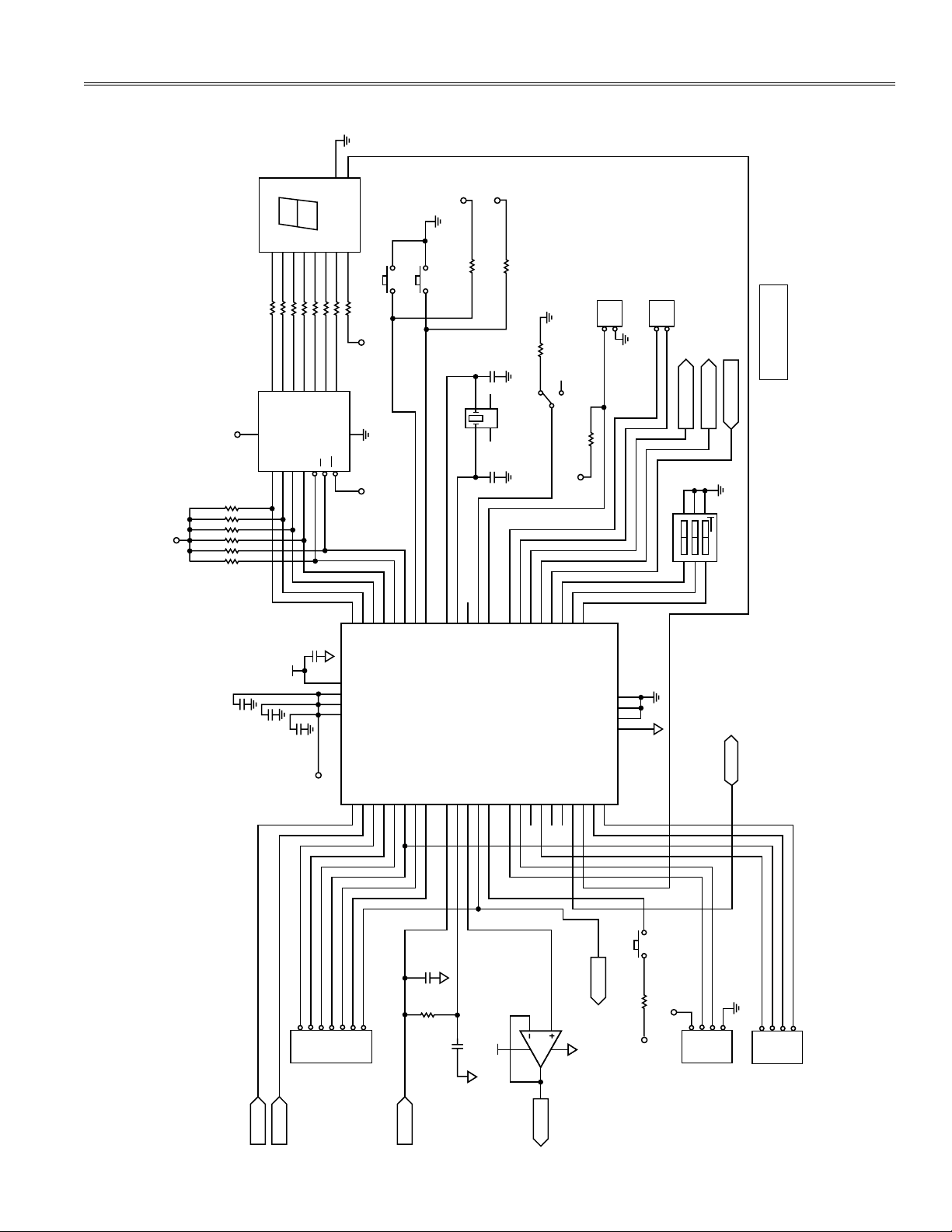
APPENDIX [A-1] SCHEMATIC–CPU
AN-655
REV. B
Figure 11. Schematic–CPU
–15–

AN-655
–17–
AN-655
TEMPOUTNCTHERMFAULT
THERMIN
TEMPSET
TEMPLOCKNCVREF
VLIM
VTEC
TEMPCTL
COMPFB
COMPOUT
PVDD
PGND
AV
DD
AG
ND
PHASE
SYNCOUT
SOFTSTART
FREQ
SYNCIN
OSC
OUTA
N1
P1
OUTB
N2
P2
SWIN
SWOUT
20
23
C2
0.1F
8
30
ADN8830
29282726252419
22
21910
11
18
17
31
32
12345
6
7
151612
13
14
LLOCK
C7
0.1F
JP1
JUMPER
1
2
R2
10k
PVDD
AVDD
C10
10nF
C9
1F
R26
1M
R27
205k
R28
100k
C14
330pF
C15
10F
R24
150k
R25
1k
PVDD
R21
10k
C5
0.1F
SD
SHORT JP1
SHUTDOWN TEC
[SD: ACTIVE LOW]
SD
A1B1Q2
CEXT2
RCEXT2
DGND
DV
CC
RCEXT1
CEXT1
Q1
Q2
B2
A2
CLR1
Q1
CLR2
U1
MM74HC123AM
PVDD PVDD
1234578
6
16
121110
9
141315
PVDD
1
2
3
4
5
U11
Y
B
A
NC7S32
NC
VINNCGND
NC
VO
UT
NC
NC
134
2
876
5
U2
ADR291GRU
AVDD
C1
0.1F
R20
10k
1%
R22
14.7k
R17
36.5k
R18
24k
R19
8.2k
TH
DAC0
TEMPLOCK
VREF
PVDD
R1
10k
C4
0.1F
R14
150
PVDD
1
2
3
Q1
FDV301N
R15
150
PVDD
1
2
32
Q2
FDV301N
D1
LED (G)
D2
LED (R)
1
R23
150k
C3
0.1F
AVDD
FDW2520C
Q5
PVDD
C6
0.1F
765
8
1
234
L1
C8
22F
CDE ESRD
TEC–
4.7F
FDW2520C
Q6
PVDD
C11
10nF
765
8
1
234
L1
C13
3.3nF
TEC+
4.7F
C12
2.2nF
REV. B
APPENDIX [A-2] SCHEMATIC–TEC CONTROL
REV. B
–16–
Figure 12. Schematic–TBC Control

APPENDIX [A-3] SCHEMATIC–LASER CONTROL
TEC–
R57
0
WLMON
VREF
AVDD
U7
AD8628ART
2
1
5
4
3
R46
2.49k
0.1%
R58
0
DAC1
LD_C
LD_C
LD_A/GND
PD1_A
PD1_C
PD2_C
PD2_A
TEC–
TEC+
TH
TH
NC
NC
GND
3
12
13
458
9
7
6
1210
14
FLD5F15
U6
AVDD
TH
TEC+
R42
0
R43
0
R45
1k
VSS
R48
5k
R41
0
VSS
R40
1.24k
VSS
283154161533226
2
IBIAS
IBIAS
IMPD
PSET
NCNCNCNCNC
ASET
GND
GND
GND
GND
GND
GND
GND
V
CC
V
CC
V
CC
V
CC
V
CC
IMPDMON
IBMON
IBMON
PAVCAP
PAVCAP
ALS
MODENCFAIL
DEGRADE
ADN2830
VSS
30
26
27
7
22
14
1
8
11
12
21
25
6
23
249102017
131918
VSS
R36
1k
VSS
R36
1k
R32
100k
VSS
R16
150
D3
LED (R)
Q4
FDV301N
1
32
2
1
IMPDMON DISABLE: R42-SHORT, R43-OPEN, R41-SHORT
IMPDMON ENABLE: R42-OPEN, R43-SHORT, R41-OPEN
R31
100k
AVDD
AD8565AKS
2
1
5
4
3
U4
VSS
VSS
R30
100k
R29
100k
IBMON
VSS
C20
0.1F
R34
10k
JP2
HEADER 2
12
R4
10k
VSS
Q3
FDV301N
Q7
FDV304P
VSS
R5
10k
R33
3k
PVDD
R3
10k
PVDD
1
1
3
2
2
3
ALS
SHORT JP2 TO
SHUTDOWN LASER
[ALS: ACTIVE HIGH]
Q7 GATE HIGH: ALS ACTIVE
Q7 GATE LOW: ALS DISABLE
C16
10nF
C17
10nF
C18
10nF
C19
10nF
VSS
11
AN-655
REV. B
Figure 13. Schematic–Laser Control
–17–
AN-655
–19–
AN-655
J1
3
2
1
TERMINAL
BLOCK
D4
LED (G)
R56
150
C29
100F
C31
22F
AVDDPVDD
L2
10F
1
2
1
2
1
2
C30
100F
C32
22F
VSS
L3
10F
2
1
2
1
–5V
REV. B
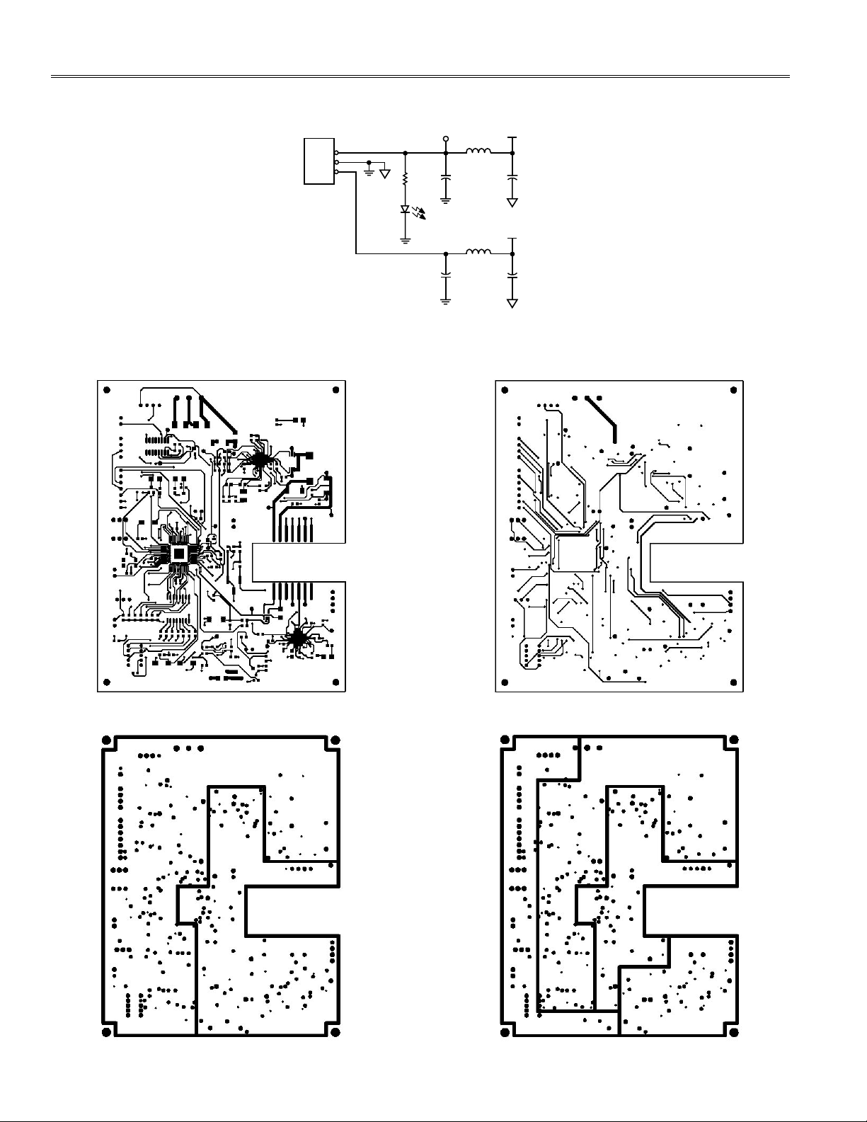
APPENDIX [A] SCHEMATIC–POWER SUPPLY
APPENDIX [B] PCB LAYOUT
Figure 14. Schematic–Power Supply
Figure 15. Top Layer
–18–
Figure 16. AGND/PGND Planes
Figure 17. Bottom Layer
Figure 18. AVDD/PVDD/VSS Planes
REV. B

Figure 19. Top Overlay
AN-655
APPENDIX [C] BILL OF MATERIALS
Provided as a software copy.
APPENDIX [D] SOFTWARE SOURCE CODE
Provided as a software copy.
REFERENCES
Analog Devices, ADuC832 Data Sheet
Analog Devices, ADN8830 Data Sheet
Analog Devices, ADN2830 Data Sheet
Fujitsu Quantum Devices, FLD5F6CA Data Sheet
Fujitsu Quantum Devices, FLD5F15CA Data Sheet
ITU-T G.692
REV. B
–19–

E03717–0–8/04(B)
Purchase of licensed I2C components of Analog Devices or one of its sublicensed Associated Companies conveys a license for the purchaser under the Philips
I2C Patent Rights to use these components in an I2C system, provided that the system conforms to the I2C Standard Specication as dened by Philips.
© 2004 Analog Devices, Inc. All rights reserved. Trademarks and registered trademarks are the property of their respective owners.
–20–
 Loading...