

Page 1
AN-641
APPLICATION NOTE
One Technology Way • P.O. Box 9106 • Norwood, MA 02062-9106 • Tel: 781/329-4700 • Fax: 781/326-8703 • www.analog.com
A 3-Phase Power Meter Based on the ADE7752
By Stephen English and Rachel Kaplan
INTRODUCTION
This application note describes a high accuracy, low cost
3-phase power meter based on the ADE7752. The meter
is designed for use in a Wye-connected 3-phase, 4-wire
distribution system. The ADE7752 may be designed into
3-phase meters for both 3-wire and 4-wire service. This reference design demonstrates the key features of an ADE7752
based meter, and is not intended for production.
The ADE7752 is a low cost single-chip solution for electrical
energy measurement that surpasses the IEC 61036 Class
1 meter accuracy requirement. It typically realizes less
than 0.1% error over a 500:1 current dynamic range for
balanced polyphase loads. The chip contains a reference
circuit, analog-to-digital converters, and all of the digital
signal processing necessary for the accurate measurement
of active energy. A differential output driver provides
direct drive capability for an electromechanical counter, or
impulse counter. A high frequency pulse output is provided
for calibration. An additional logic output on the ADE7752,
REVP, indicates negative active power on any phase or a
possible miswiring. The ADE7752 data sheet describes
the device’s functionality in detail and is referenced several
times in this document.
DESIGN GOALS
Specifi cations for this Class 1 meter design are in accordance
with the accuracy requirements of IEC 61036, and Indian
Standards IS 13779-99. Tables I and II review the overall
accuracy at unity power factor and at low power factor.
Table I shows the specifi cations of the meter for both balanced loads and balanced lines. Table II addresses balanced
polyphase voltages with a single-phase load.
The meter was designed for an I
of 50 A/phase, an Ib of
MAX
5 A/phase, and a 100 impulses/kWh meter constant. The
ADE7752 provides a high frequency output at the CF pin.
This output is used to speed the calibration process and
provide a means of quickly verifying meter functionality
and accuracy in a production environment. CF is 16 times
F1, F2, the frequency outputs. In this case, CF is calibrated
to 1600 impulses/kWh. The meter is calibrated by varying the attenuation of the line voltage using the resistor
networks on each phase. Each phase to neutral voltage is
240 V. See the Channel 2 Input Network section.
An additional specifi cation for this meter design is taken
from IS 13779-99. The specifi cation states that the meter
must work with only one phase active at 30% lower and
20% higher than the nominal line value.
Table I. Accuracy Requirements
(for a polyphase balanced load)
Percentage Error Limits3
Current Value
1
PF2 Accuracy
Class 1 Class 2
0.05 Ib £ I < 0.1 Ib 1 ±1.5% ±2.5%
0.1 I
0.1 I
£ I < I
b
£ I < 0.2 Ib
b
1 ±1.0% ±2.0%
MAX
0.5 inductive
±1.5% ±2.5%
0.8 capacitive ±1.5%
NOTES
1
The current ranges for specifi ed accuracy shown in Table I are expressed
in accordance with IEC 61036, Table 15 percentage error limits, Section 4.6.1, p. 53.
2
Power factor (PF) in Table I relates to the phase relationship between the
fundamental voltage and current waveforms. In this case, PF can be
defi ned as PF = cos(), where is the phase angle between pure sinusoidal
current and voltage.
3
Accuracy is defi ned as the limits of the permissible percentage error. The
percentage error is defi ned as:
Percentage Error
energy registered by meter –true energy
=×
Table II. Accuracy Requirements
true energy
*
100%
(1)
(for a polyphase meter with single-phase load)
Percentage Error Limits
Current Value PF
Accuracy
Class 1 Class 2
0.1 Ib £ I < I
£ I < I
0.2 I
b
1 ±2.0% ±3.0%
MAX
MAX
0.5 inductive
±2.0% ±3.0%
REV. 0
*
Accuracy class for unbalanced load as defi ned in IEC 61036, Table 13,
Section 4.6.1, p. 53, Edition 2.1.
Page 2
AN-641
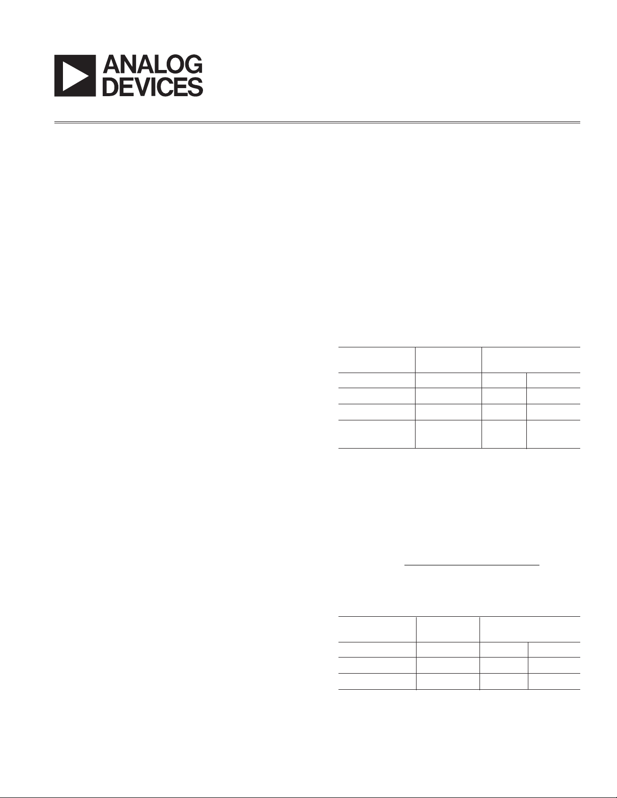
Figure 1 is a block diagram of a low cost, simple watthour
meter using the ADE7752. It shows the three phases and
how they are connected to the meter. Three current transformers sense the load current and convert the signals to
a proportional voltage required by the ADE7752. The total
energy is registered by a mechanical counter.
240V 240V
240V
MECHANICAL
COUNTER
VAP VBP
N VCP
16
15
14
5
6
7
ADE7752
8
9
10
13
1
CF
24
23
4
REVP
LOAD
ATTENUATION
NETWORKS
ANTI-
ALIASING
FILTERS
ANTI-
ALIASING
FILTERS
ANTI-
ALIASING
FILTERS
Figure 1. 3-Phase, 4-Wire/Wye Watthour Meter Block
Diagram
DETAILED DESCRIPTION
The front end of the meter is made up of three pairs
of voltage and current input networks. Each of the three line
voltages is attenuated and fi ltered through identical antialiasing fi lters. See the Channel 2 Input Network section.
The current channels’ signals are converted from current
to a voltage through current transformers and burden
resistors. The signals are then fi ltered by the antialiasing
fi lter on each of the three phases, and the result is applied
to the current inputs of the ADE7752.
Each phase of the meter has a power supply associated
with it. The power supply is shown in Figure 8. If power
is lost in two of the three phases, the meter will continue
to operate. Each phase has a corresponding LED that is
on when the respective phase is active.
A calibration network is associated with each of the three
line voltages. These circuits use binary-weighted resistor
values connected in series to set the amount of attenuation
needed for each of the three input voltages. Having ±25%
calibration ability to compensate for variations in the voltage reference and input fi lter components is recommended.
See the Design Calculations section.
An opto-isolator is provided on this meter, connected to
the CF pin of the ADE7752. This allows calibration of the
meter while isolating the calibration equipment from the
line voltages.
The instantaneous power and energy are calculated per
phase, and the net active energy is accumulated as a sum
of the individual phase energies inside the ADE7752. With
the ABS pin set low, the sum represents the absolute values
of the phase energies. With the ABS pin high, the ADE7752
takes into account the signs of the individual phase energies
and performs a signed addition. In the meter described in
this application note, ABS is set high.
If negative active power is detected on any of the three
phases, the REVP output LED of the ADE7752 is lit. This
feature is useful to indicate meter tampering or to fl ag
installation errors. The ADE7752 continues to accumulate
energy despite the status of the REVP output pin. REVP will
reset when positive power is detected again. The output
of REVP and the CF pulse are synchronous. If more than
one phase detects negative power, the REVP LCD remains
lit until all phases detect positive power.
An LED connected to the CF output of the ADE7752 displays
the energy measured in impulses/kWh. The ADE7752 data
sheet describes this operation in detail. The frequency outputs, F1 and F2, are used to drive the electromechanical
counter. See the Design Equations section.
This design has a startup current of 13.75 mA and a no-load
threshold of 3.3 W. See the Starting Current section.
DESIGN EQUATIONS
The ADE7752 produces an output frequency that is proportional to the summed values of the three phase energies.
A detailed description of this operation is available in the
ADE7752 data sheet. To calibrate the meter, the inputs to
the ADE7752 must be defi ned based on the equation:
VIVIV I F
××+×+×
22
()
11 2 2 3 3 17
2
V
REF
×
−
(2)
FF
12
, =
5.9
where:
I is the differential rms voltage signal on respective current channels
V is the differential rms voltage signal on respective voltage channels
is the reference voltage (2.4 V ± 8%) (V)
V
REF
is one of fi ve possible frequencies selected by using
F
1–7
the logic inputs SCF, S0, and S1. See Table II.
The calculations for this meter design are shown in the
Design Calculations section.
ADE7752 REFERENCE
Pin 12 of the ADE7752 can be used to connect an external
reference. This design does not include the optional reference circuit and uses the ADE7752 internal reference.
–2–
REV. 0
Page 3
AN-641
The on-chip reference circuit of the ADE7752 has a typical
temperature coeffi cient of 20 ppm/°C. Refer to the ADE7752
data sheet for graphs of typical performance characteristics
over temperature.
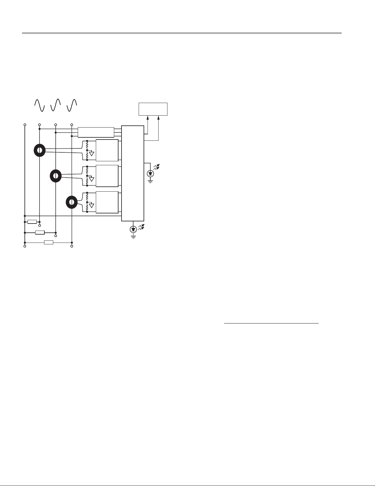
Current Transformer Selection
The current transformer is the device used in this design for
measuring load current. This sensor arrangement provides
isolation because the line-to-line voltage differs by more
than 498 V. Current transformers offer an advantage as
current sensors because they do not contact the conductor,
they handle high current and have low power consumption
and low temperature shift. Figure 3 illustrates the application used in this design for each channel of the 3-phase
meter. When selecting a current transformer, carefully
evaluate linearity under light load. The CT performance
should be better than the desired linearity of the meter
over the current dynamic range.
A current transformer uses the concept of inductance to
sense current. A CT is made up of a coil wound around
a ferrite core. The current-carrying wire is looped through
the center of this winding, which creates a magnetic fi eld
in the winding of the CT and a voltage output proportional
to the current in the conducting wire. The properties that
affect the performance of a given CT are the dimensions of
the core, the number of turns in the winding, the diameter
of the wire, the value of the load resistor, and the permeability and loss angle of the core material.
When choosing a CT, consider the dc saturation level. At
some high, fi nite value of current or in the presence of a
high dc component, the ferrite core material exhibits hysteresis behavior and the CT can saturate. Manufacturers
of CTs can specify this maximum level. The current range
is calculated using Equation 3.
I
MAX
2
N
ω
sec
R
BA
sat Fe
(3)
≈
where:
R is the resistance of the burden resistor and the copper wire
A
Fe
B
sat
.
represents the dimensions of the core.
is the value of the magnetic fi eld at which the core
material saturates.
is the number of turns in the CT.
N
sec
CTs may also cause a phase shift of the signal. A CT used
for metering should have a linear phase shift across the
desired current dynamic range. The phase error for a CT
is derived using Equation 4.
R
cosϕ
tan
δ=
L
ω
(4)
where:
R is the resistance of the burden resistor and the copper wire.
␦ represents the core losses.
L is a parameter based on the permeability of the core,
the dimensions of the core, and the square of the number
of turns.
The phase error caused by a particular CT should be measured with and compensated for by a low-pass fi lter before
the ADC inputs. Phase mismatch between channels will
cause energy measurement errors. See the Correct Phase
Matching between Channels section. Low-pass fi lters are
already required by the ADE7752 for antialiasing, and are
covered in more detail in the Antialias Filters section. The
corner frequency of these antialiasing fi lters on the current
channels can be fi ne tuned by changing the components
in the RC circuit in order to add additional compensation
for CT phase shift.
Channel 1 Input Network
Figure 3 shows the input stage to Channel 1 of the meter.
The current transformer has a turns ratio of 1500:1. The
burden resistor is selected to give the proper input voltage range for the ADE7752, less than 500 mV
PEAK
. See the
Design Calculations section. The additional components
in the input network provide fi ltering to the current signal.
The fi lter corner is set to 4.8 kHz for the antialias fi lters.
See the Antialias Filters section.
PHASE A
LOAD
CURENT
CURRENT TRANSFORMER
R82
R83
R15
R17
IAP
C16
IAN
C17
Figure 2. ADE7752 Phase A – CT Wiring Diagram
The burden is center tapped so that external capacitive
coupling may be reduced. The wires of the CT are twisted
tightly to reduce noise.
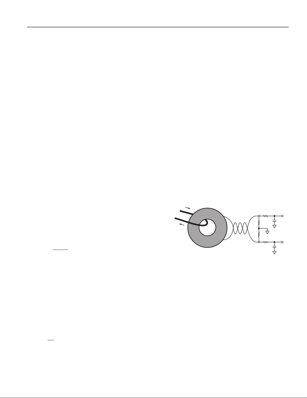
Channel 2 Input Network
The meter is calibrated by attenuating the line voltage
down to 70 mV. See the Design Calculations section. The
line voltage attenuation is carried out by a resistor divider
as shown in Figure 4. Phase matching between Channel
1 and Channel 2 is important to preserve in this network.
Figure 4 shows the attenuation network for the voltage
inputs. All three phases have the same attenuation network. The –3 dB frequency of this network, on Phase A
for example, is determined by R75 and C21 because the
sum of the other resistors in the network is much greater than
R75. The approximate equation is shown in Figure 3.
REV. 0
–3–
Page 4
AN-641
PHASE A
240V
R80 R81
R66
R68
R70
R79
R76
R64
R65
R78
R73
R75
f
= (2 ⴛ R75 ⴛ C21)
–3dB
C21
VAP
70mV
Figure 3. Attenuation Network
Because the ADE7752 transfer function is extremely linear,
a one-point calibration (I
) at unity power factor is all that is
b
needed to calibrate the meter on each phase. If the correct
precautions were taken at the design stage, no calibration
is necessary at low power factor (PF = 0.5).
CORRECT PHASE MATCHING BETWEEN CHANNELS
Correct phase matching is important in energy metering
applications because any phase mismatch between channels will translate into signifi cant measurement error at
low power factor. The errors induced in the system at
PF = 1 are minimal. A power factor of 0.5 with a phase
error of as little as 0.5
°
will cause a 1.5% error in the
power measurement. If current lags the voltage by 60°
(PF = –0.5) and pure sinusoidal conditions are assumed,
the power is easily calculated, on a single phase, as
V rms ⫻ I rms ⫻ cos(60°).
An additional phase error can be introduced to the overall
system with the addition of antialiasing fi lters. Phase error
(
) is introduced externally to the ADE7752 (e.g., in the
e
antialias fi lters). The error is calculated as
%Error cos – cos cos 100%
=° +
[]
e
°×() ( )/ ()δδφ δ
(5)
See Note 3 for Table I, where ␦ is the phase angle between
voltage and current and
is the external phase error.
e
With a phase error of 0.2°, for example, the error at PF = 0.5
inductive (60°) is calculated as 0.6%. As this example demonstrates, even a very small phase error will produce a
large measurement error at low power factor.
Current transformers often produce a phase shift between the
current and voltage channels. To reduce the error caused
at low power factor, the resistors in the antialias fi lter can
be modifi ed to shift the corner frequency of the fi lter (in the
current channel), introducing more or less lag.
The antialias
fi lters are described in detail in the next section.
The phase error should be measured independently on
each phase (A,
B, and C). To calibrate the phase error
on one phase of the meter, a two-point measurement
is required. The fi rst measurement should be at the test
current, I
, with unity power factor and the second at low
b
power factor (0.5 capacitive). The measurement error is
processed according to the following equation:
CF
PF
=1
Error
CF
=
–
PF
= 0.5
CF
2
PF
=1
2
(6)
The phase error is then:
Phase Error arcsin
= –
Error
3
(7)
For a single-pole RC low-pass fi lter, the phase lag is:
θπ=–arctan 2 fRC×
()
(8)
For example, if the antialias fi lters are single-pole lowpass fi lters with R = 1 k⍀ and C = 33 nF, the phase lag at
50 Hz is 0.59° according to Equation 8. If the measurements performed with this fi lter in place on the current
and voltage phases show that the CT causes 1° phase error
(using Equations 6 and 7), then the resistor value should be
2.68 k⍀ to give 1.59° total phase shift. Because there is
generally minimal part-to-part variation for CTs, the same
fi lters usually can be used in production on all three phases
to compensate for the constant phase error.
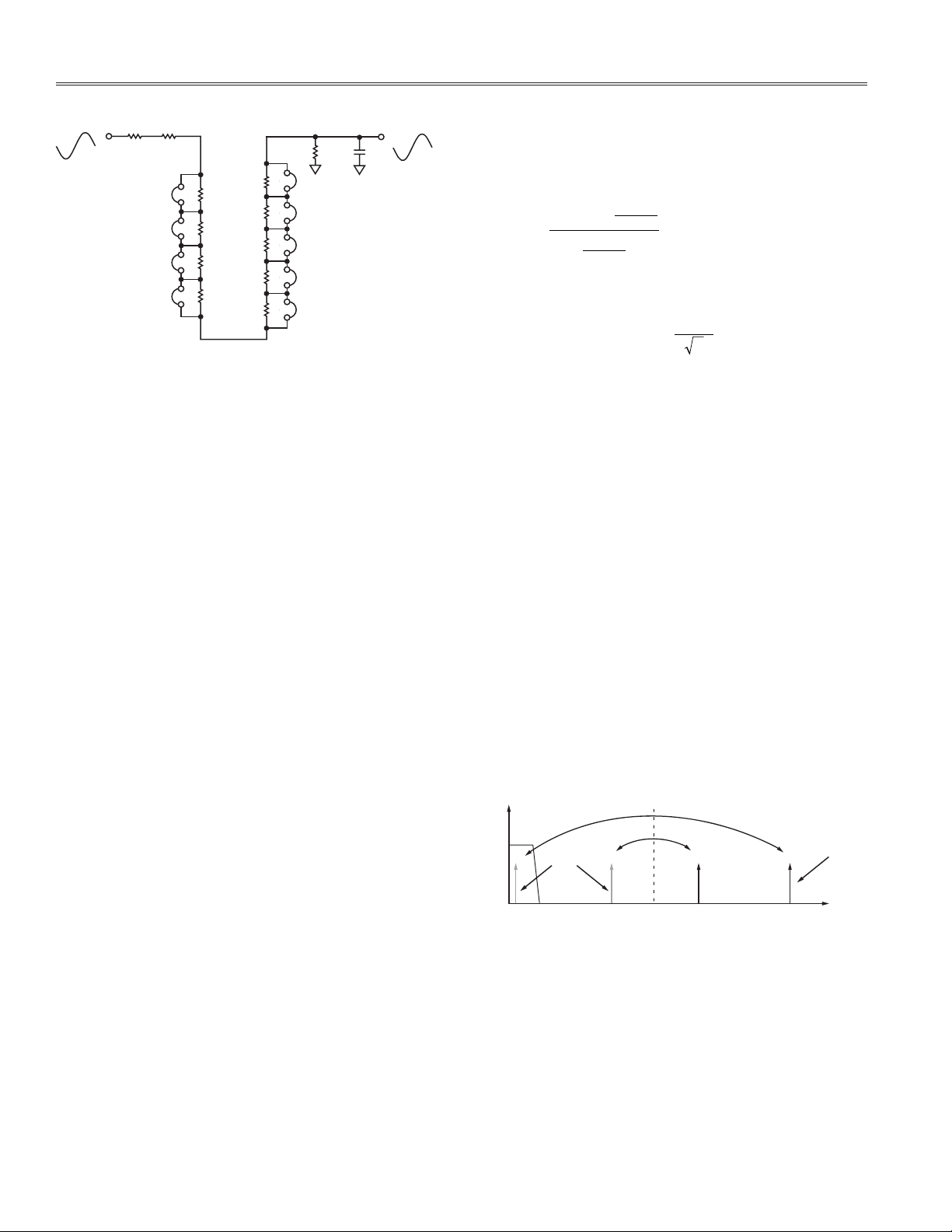
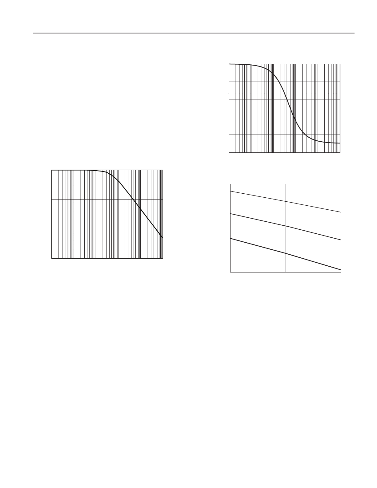
ANTIALIAS FILTERS
As mentioned in the previous section, one possible source
of external phase errors is the antialias fi lters on the input
channels. The antialias fi lters are low-pass fi lters placed
before the analog inputs of any ADC. They are required
to prevent aliasing, a possible distortion due to sampling.
Figure 4 illustrates the effects of aliasing.
ALIASING EFFECTS
IMAGE
FREQUENCIES
SAMPLING
FREQUENCY
0 2 417
FREQUENCY (kHz)
833
Figure 4. Aliasing Effects
Figure 4 shows how aliasing effects could introduce
inaccuracies in an ADE7752 based meter design. The
ADE7752 uses two ⌺-⌬ ADCs to digitize the voltage and
current signals for each phase. These ADCs have a very
high sampling rate, i.e., 833 kHz. Figure 4 shows how
frequency components (indicated by the darker arrows)
above half the sampling frequency (also known as the
Nyquist frequency), i.e., 417 kHz, get imaged or folded back
down below 417 kHz (indicated by the gray arrows). This
will happen with all ADCs, regardless of the architecture.
–4–
REV. 0
Page 5
AN-641
In the example shown, only frequencies near the sampling
frequency, i.e., 833 kHz, will move into the band of interest
for metering (0 kHz to 2 kHz). This fact
very simple LPF (low-pass fi lter) to attenuate
allows the use of a
these high
frequencies (near 833 kHz) and thus prevent distortion in the
band of interest. The simplest form of LPF is the simple RC
fi lter, which has a single pole with a roll off or attenuation
of –20 dBs/decade.
Choosing the Filter –3 dB Frequency
In addition to having a magnitude response, fi lters also h ave
a phase response. The magnitude and phase response
of a simple RC fi lter (R = 1 k⍀, C = 33 nF) are shown in
Figures 5 and 6. Figure 5 shows that the attenuation near
900 kHz for this simple LPF is greater than 40 dBs. This is
suffi cient attenuation to ensure that no ill effects are caused
by aliasing.
0dB
–20dB
–40dB
frequency components to be aliased and cause accuracy
problems in a noisy environment.
0
–20
–40
–60
PHASE (Degrees)
–80
–100
10 100 1k 100k10k 1M
FREQUENCY (Hz)
Figure 6. RC Filter Phase Response
–0.4
(50Hz, –0.481)
–0.5
–0.6
(R = 900⍀, C = 29.7nF)
(50Hz, –0.594)
(R = 1k⍀, C = 33.0nF)
–60dB
10 100 1k 100k10k 1M
FREQUENCY (Hz)
Figure 5. RC Filter Magnitude Response
The phase response can introduce signifi cant errors if the
phase response of the LPFs on both current and voltage
channels are not matched. This is true for all of the phases
in which the desired (120°) phase shift between phases
should be preserved. Phase mismatch can easily occur
as a result of poor component tolerances in the LPF. The
lower the –3 dB frequency in the LPF (antialias fi lter), the
more pronounced these errors will be at the fundamental
frequency component or line frequency. Even with the corner frequency set at 4.8 kHz (R = 1 k⍀, C = 33 nF), the phase
errors due to poor component tolerances can be signifi cant.
Figure 7 illustrates this point.
In Figure 6, the phase response for the simple LPF is
shown at 50 Hz for R = 1 k⍀ ± 10%, C = 33 nF ± 10%.
Remember,
a phase shift of 0.2° can cause measurement
errors of 0.6% at low power factor. This design uses resistors of 1% tolerance and capacitors of 10% tolerance for
the antialias filters to reduce the likelihood of problems
resulting from phase mismatch. Alternatively, the corner
frequency of the antialias filter could be pushed out to
10 kHz to 15 Hz. The corner frequency should not be made
too high, however, because doing so could allow high
PHASE (Error)
–0.7
–0.8
45 50 55
FREQUENCY (Hz)
(50Hz, –0.718)
(R = 1.1k⍀, C = 36.3nF)
Figure 7. Phase Shift at 50 Hz Due to Component
Tolerances
Note that this risk is also why precautions were taken
with the design of the calibration network on the voltage
channels. The tolerance of the components used in these
networks is low to prevent errors.
CALIBRATING THE METER
The meter is calibrated by setting the appropriate value
to the S1 and S0 pins and by varying the gains of the voltage channels. The current channels are fi xed by the turns
ration of the CT and the burden resistor.
To ensure the proper output frequency, the meter is
calibrated using CF. The gains of the voltage channels
are varied to ensure that the product of the current and
voltage channels (active energy) is calibrated to 1600
impulses/kWh. The voltage channel uses a resistor divider
network to adjust the attenuation. The setup of this network
is described in the Channel 2 Input Network and Design
Calculations sections.
REV. 0
–5–
Page 6

AN-641
DESIGN CALCULATIONS
The goal of the design calculations is to achieve appropriate
input signal levels for the Channel 1 and Channel 2 ADCs.
Each channel requires a voltage input less than 500 mV
PEAK
The input levels should be set up so that the full dynamic
range of current results in a frequency output on F1, F2 that
will drive the stepper motor counter.
The frequency outputs can be calculated using Equation 1
set equal to the maximum output frequency, which corresponds to the nominal line voltage and maximum current.
To use Equation 9 for calculating the Channel 2 input level,
fi x the Channel 1 input level to some percentage of full scale
and choose an appropriate F
data sheet. This F
to be less than 500 mV
value should allow the voltage input
1–7
PEAK
value from the ADE7752
1–7
.
Since the current channel requires a voltage input, a burden resistor is used to yield the calculated input level.
The line voltage must be trimmed with a resistor network
to the appropriate ADC input level.
Calculate F1, F2, and CF
The frequency for F1 and F2 can be calculated using
Equation 9.
VIVIV I F
××+×+×
()
22 33
2
V
REF
×
−11 17
(9)
F1,F2
=
5.922
Design parameters:
Line voltage = 240 V
V
= 240 V rms + 20% = 288 V rms
MAX
Class 100 meter with I
(each phase to neutral)
rms
= 50 A rms
MAX
Meter constant = 100 impulses/kWh
CF = 1600 impulses/kWh
CT turns ratio (CT
) = 1500:1
TRN
There are 10 different choices of frequency output through
SCF, S1, and S0 pins. To choose the proper frequency, the
maximum F1, F2 frequency output using the line voltage
and I
must be calculated. For three phases at maximum
MAX
power, where
POWER
F1, F2
= 3 ⫻ 50 A rms ⫻ 240 V rms = 36 kW
MAX
= 100 impulses/kWh ⫻ 36 kW = 3600 impulses/H
MAX
= 3600 impulses/H ⫻ 1 H/3600S = 1 Hz
At maximum current, the input signal at the current channel
should be some fraction of full scale to allow headroom.
Equation 1 can be used to choose an H frequency by
fixing the current input to be 60% of full scale rms,
215 mV rms.
5.9 3 0.215
1
Hz
22
=
VF
×× ×
()
2.4
()
×
2
1– 7
(10)
Choose F
to fi nd the corresponding input voltage. In this case, F
is 4.77, so V = 0.105 V. Other values for F
.
reasonable results for the voltage, i.e. some fraction of
from Table III. The expression can be evaluated
1–7
do not yield
1–7
1–7
full scale rms input to allow for headroom; 105 mV is 30%
of the full scale rms voltage input. The following calculation demonstrates that suffi cient headroom is achieved
if the voltage input that results with the maximum line
voltage (288 V rms
full scale ADC input
from the IS Specifi cation) is below the
level (500 V
PEAK
or 353
V rms
). For
three phases at maximum power, where
POWER
F1, F2
= 3 ⫻ 50 A
MAX
= 100 impulses/kWh ⫻ 43.2 kW = 4320 impulses/H
MAX
⫻ 288 V rms = 43.2 kW
rms
= 4320 impulses/H ⫻ 1 H/3600S = 1.2 Hz
Plugging 1.2 Hz into Equation 9 and solving for the voltage
with F
= 4.77, as done in the previous calculation, the
1–7
voltage input is 126 mV. This value is 36% of the full-scale
rms voltage input. With F
of 4.77 selected, suffi cient
1–7
headroom has been achieved.
Max F1/F2 is chosen as 1.83 Hz with S1 = 0 and S0 = 1.
Table III in the ADE7752 data sheet shows the choices for
Max F1/F2.
The desired CF in this case is 1600 impulses/kWh. Knowing that CF = k ¥ F1, F2 = 1600 impulses/kWh = 16 ⫻ 100
impulses/kWh; SCF is chosen to be 1 so that the meter
constant is 16 times that of the stepper motor ratio.
Table III. F
Frequency Selections and Max Output Frequency
1–7
Max F1/F2 Max CF
SCF S1 S0 F
(Hz) (Hz)
1–7
0 0 0 1.27 0.49 78.19
1 0 0 1.19 0.46 3.66
0 0 1 5.09 1.95 312.77
1 0 1 4.77 1.83 29.32
0 1 0 19.07 7.33 117.30
1 1 0 19.07 7.33 58.65
0 1 1 76.29 29.32 234.59
1 1 1 0.60 0.23 3.67
Calculate R
BURDEN
At maximum current, the voltage input signal at the current channel is:
I
/CT
RMS
VIN = 500 mV
R
BURDEN
= 50 A rms/1500 = 33.33 mA rms
TRN
or 353.6 mV rms; 60% V rms = 215 mV rms
PEAK
= 215 mV rms/33.33 mA rms = 6.45 ⍀
Since the input signal is differential for each channel, the
burden resistor is split in two to yield 3.23 ⍀ ¥ 2.
–6–
REV. 0
Page 7
AN-641
Calculate Attenuation Network
Each phase will have the same attenuation network. From
Equation 9, V = 105 mV rms. The line voltage of 240 V must
be trimmed to this value. The attenuation network is calculated to be 240 V/105 mV or an attenuation of 2285:1.
POWER SUPPLY DESIGN
The IEC 61036 specifi cation requires the meter to have a
mean power consumption of 2 W or 10 VA for a polyphase
meter. The IS specifi cation for the power supply is 1 W per
voltage channel. Another key specification that relates
to power supply design requires the power supply to
operate with only one phase active at 70% of nominal.
The line voltage may vary from –30% to +20%, in accordance with the Indian standard.
The current drawn from the power supply at the regulator, VR1, output with no load is 9.75 mA. When the
stepper motor engages (with a 10 A load applied),
the current draw increases by 15 mA. The result is
approximately
25 mA of current draw at 5 V. This is
equivalent to 0.125 W of peak power consumption.
The current draw of one phase of the meter is 10 mA, mea sured at the line input. At 240 V w ith all three pha ses running,
the total power consumption of this design is 7.2 VA.
Since the line voltage varies from 168 V to 288 V, a power
supply that will work over this extended range is needed.
This design uses a power supply based on three power
transformers that transfer power rather than current or
voltage. For this reason, as the line voltage decreases,
the current increases, keeping the power used by the
supply constant. Figure 8 shows a diagram of the power
supply circuit.
The supplies for this meter are three full wave rectifi ed
supplies connected in parallel through diodes. The output
of this circuit is then fi ltered and regulated to 5 V.
The MOV-Ferrite bead at the input to the power supply is
used to minimize the effect of electrical fast transients. Large
differential signals may be generated by the inductance
of the PCB traces and signal ground. These large signals
may affect the operation of the meter. The analog sections
of the meter will fi lter the differential signal and minimize
the effect on the duration of the pulse.
The ferrite and capacitor create a low-pass fi lter before the
MOV. In an EFT event, this ensures protection during the small
time it takes for the MOV to turn on. For more information
concerning this issue, see Application Note AN-559.
An LED on each phase of the power supply indicates the
status of power on that phase. Blocking diodes prevent
the LED from lighting when the voltage to the phase is
shorted. Without this diode, current fl ow from the other
phases could light the indicator LED. At the output of the
regulator, C12 and C2 fi lter ripple that could degrade the
performance of the power supply.
240V
PHASE A
240V
PHASE B
240V
PHASE C
L3
V1
C1
L2
V2
C2
L1
V3
C24
T3
T2
T1
CR3
CR2
CR1
1k⍀
1k⍀
1k⍀
VR1
7805
C12
VDD
+
+
5V
C2
–
Figure 8. Power Supply
REV. 0
–7–
Page 8
AN-641
STARTING CURRENT
The no-load threshold and start-up current features of the
ADE7752 eliminate creep effects in the meter. A load that
generates a frequency lower than the minimum frequency
will not result in a pulse on F1, F2, or CF. The minimum
output frequency is defi ned in the ADE7752 as 0.005% of
the full-scale output frequency (F1, F2) for the F
tion. For this meter, the minimum output frequency on
F1, F2 is 9.15 ⫻ 10
impulses/kWh.
(100 impulses/kWh)(1 H/3600)(P) = 9.15 ⫻ 10
The minimum load then becomes 3.3 W, which translates
to 13.75 mA of startup current at 240 V.
The IEC specifi cation for the no-load threshold, Section
5.6.4, states that the meter should not register a pulse for
a specifi ed time with the voltage at 115% V
circuit current. The no-load threshold described above for
the ADE7752 ensures compliance with this specifi cation.
The IEC specifi cation, section 4.6.4.3, for start-up current
is 0.4% of I
specifi cation, the meter must start and continue to register
current at this level. The design of the meter described in
this application note meets this specifi cation by starting
up at 13.75 mA, as calculated.
, or 40 mA with an Ib = 10 A. According to the
b
–5
Hz, and the meter constant is 100
1–7
–5
Hz
and open
REF
selec-
ADE7752 REFERENCE DESIGN PERFORMANCE
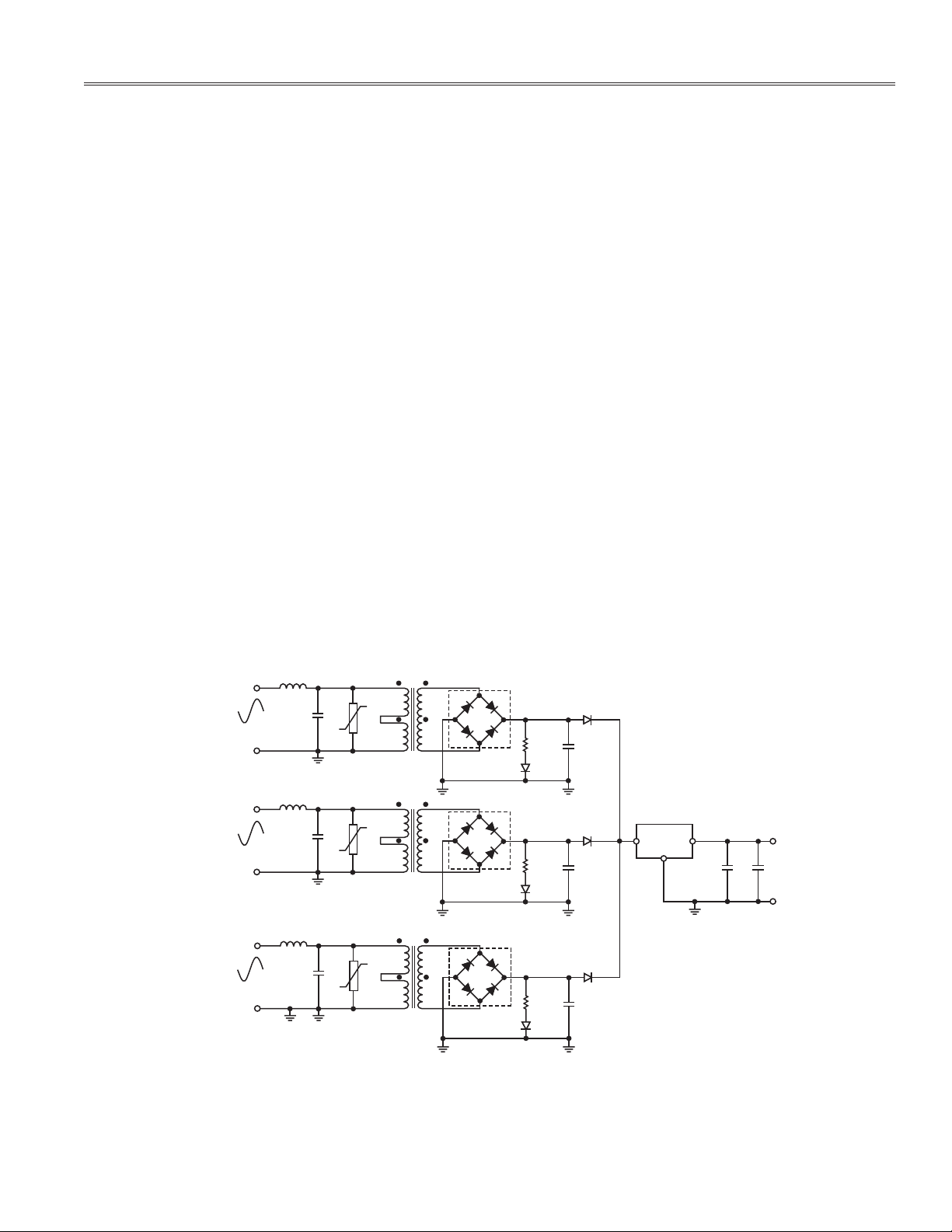
This reference design surpasses the IEC 61036 Class 1
accuracy requirements, as outlined in Section 4.6.1 of the
IEC 61036 standard. The typical performance plots shown
demonstrate the performance of this reference design
against the IEC accuracy limit. Voltage and frequency
variation tests were performed according to Section 4.6.2
of the IEC 61036 standard.
Figure 9. Final Implementation of ADE7752
Reference Design
–8–
REV. 0
Page 9

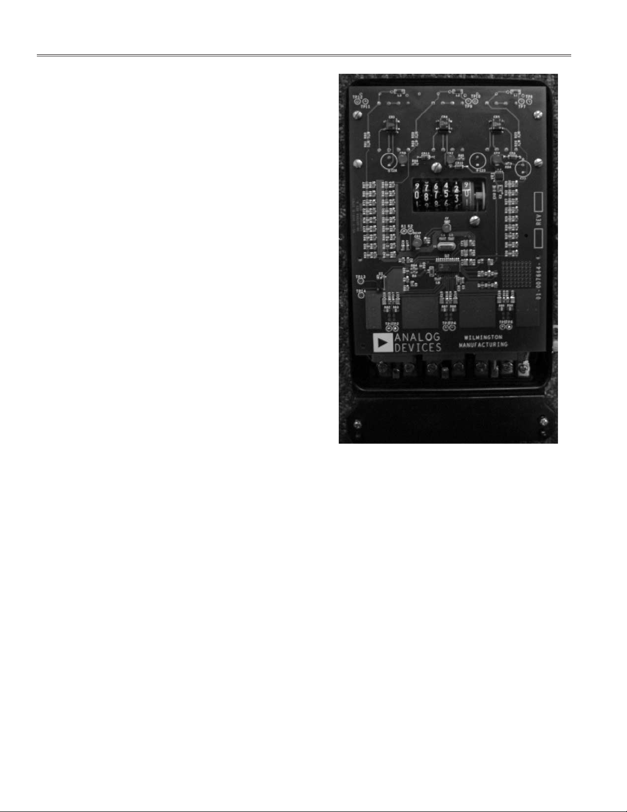
AN-641
2.0
1.5
1.0
0.5
0
ERROR (%)
–0.5
–1.0
–1.5
–2.0
0.1 1.0
CURRENT (A)
BALANCED LOAD
PF = 1
IEC 61036 4.6.1
IEC LIMIT
PF = 1
IEC LIMIT
10 100
TPC 1. Balanced Polyphase Load with Unity Power Factor
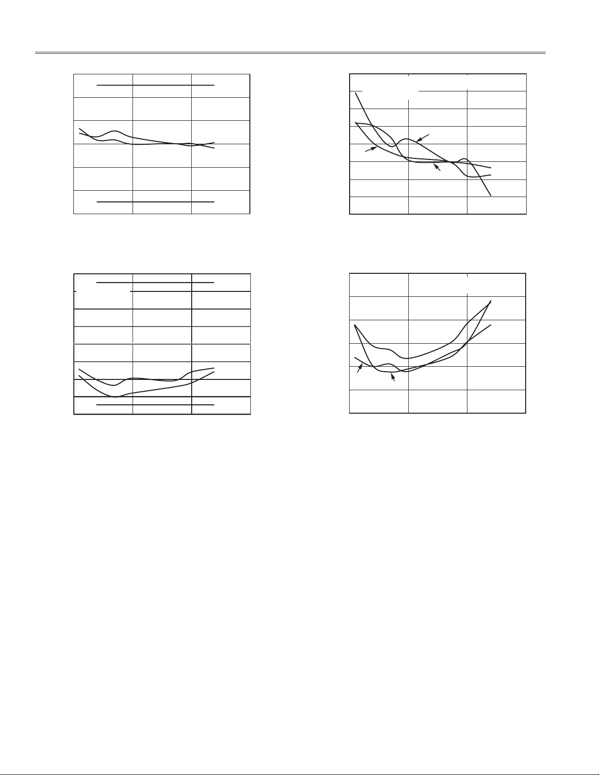
2.0
BALANCED LOAD
IEC 61036 4.6.1
1.5
1.0
0.5
0
ERROR (%)
–0.5
IEC LIMIT
PF = 0.8 CAP
PF = 0.5 IND
0
UNBALANCED LOAD
PF = 0.5
–0.1
IEC 61036 4.6.1
–0.2
–0.3
–0.4
ERROR (%)
–0.5
–0.6
–0.7
0.1 1.0
CURRENT (A)
IEC LIMIT = ⴞ2%
PHASE C
ONLY
PHASE B
ONLY
PHASE A
ONLY
10 100
TPC 4. Unbalanced Load over Power Factor
0.8
0.6
0.4
0.2
0
ERROR (%)
–0.2
BALANCED LOAD
PF = 1
IEC 61036 4.6.2
216V
264V
IEC LIMIT
–1.0
–1.5
–2.0
0.1 1.0
CURRENT (A)
IEC LIMIT
10 100
TPC 2. Balanced Polyphase Load over Power Factor
0.30
UNBALANCED LOAD
PF = 1
0.25
IEC 61036 4.6.1
0.20
0.15
0.10
ERROR (%)
0.05
0
–0.05
–0.10
0.1 1.0
PHASE A
ONLY
PHASE C
ONLY
PHASE B
ONLY
CURRENT (A)
IEC LIMIT = ⴞ2%
10 100
TPC 3. Unbalanced Load with Unity Power Factor
–0.4
–0.6
–0.8
0.1 1.0
CURRENT (A)
10 100
TPC 5. Voltage Variation ±10% from 240 V
with Unity Power Factor
1.5
BALANCED LOAD
PF = 0.5
IEC 61036 4.6.2
1.0
0.5
0
ERROR (%)
–0.5
–1.0
–1.5
0.1 1.0
264V (240V+10%)
216V (240V–10%)
10 100
CURRENT (A)
TPC 6. Voltage Variation ±10% from 240 V
with Power Faction = 0.5 Inductive
IEC LIMIT
IEC LIMIT
IEC LIMIT
REV. 0
–9–
Page 10
AN-641
0.6
BALANCED LOAD
PF = 1
IEC 61036 4.6.2
0.4
0.2
0
ERROR (%)
–0.2
–0.4
–0.6
0.1 1.0
49Hz
51Hz
10 100
CURRENT (A)
IEC LIMIT
IEC LIMIT
TPC 7. Frequency Variation ±2% from 50 Hz
with Unity Power Factor
0.8
BALANCED LOAD
0.6
PF = 0.5
IEC 61036 4.6.2
0.4
0.2
0
ERROR (%)
–0.2
–0.4
–0.6
–0.8
0.1 1.0
CURRENT (A)
10 100
IEC LIMIT
51Hz
49Hz
IEC LIMIT
0.25
BALANCED LOAD
PF = 0.5
0.20
IS 13779:1999 11.2
0.15
0.10
0.05
192V
ERROR (%)
0
–0.05
–0.10
–0.15
0.1 1.0
288V
CURRENT (A)
IS LIMIT –30% = ⴞ3.5%
IS LIMIT ⴞ20% = ⴞ2.1%
168V
10 100
TPC 9. Indian Standard Voltage Variation +20%
and –30% from 240 V with Unity Power Factor
–0.1
BALANCED LOAD
PF = 0.5
IS 13779:1999 11.2
–0.2
–0.3
–0.4
ERROR (%)
–0.5
288V
–0.6
–0.7
0.1 1.0
168V
CURRENT (A)
IS LIMIT –30% = ⴞ5%
IS LIMIT ⴞ20% = ⴞ3%
192V
10 100
TPC 8. Frequency Variation ±2% from 50 Hz
with Power Factor = 0.5 Inductive
TPC 10. Indian Standard Voltage Variation +20% and
–30% from 240 V with Power Factor = 0.5 Inductive
–10–
REV. 0
Page 11
VDD
AN-641
C2
10F
25V
AGND
TP14
TP13
3
4
NECP52501-1
U1
2
1
DGND
RED
CR2
R11
825⍀
C1
1F
DGND
DGND
C5
22pF
R2
2322212019181716151413
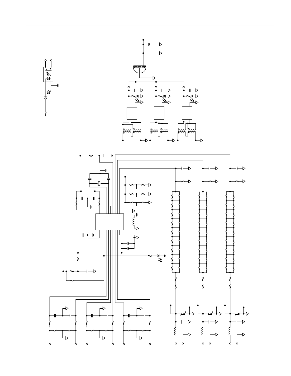
F2
S0
S1
VAP
SCF
VBP
ABS
CLKIN
CLKOUT
DGND
VDD
REVP
IAP
IAN
IBP
IBN
ICN
3456789
2
AGND
ICP
101112
VDD
R3
R92
R12
VDD
R1
0⍀
R91
0⍀
0⍀
1.02k⍀
C4
22pF
Y1
10mHz
K1
K2
C6
C7
DGND
0.1F
0.1F
24
F1
CF
1
C8
0.1F
DGND
C9
0.1F
VCP
AGND
51
T3
VNREF
UA7BL05ACD
CR11
1
+
CR3
PHASE A
AGND
VAL
REFDES–U2
C10
0.1F
+
AGND
VR1
⍀
R86
1.18k
AC2
62
R80⍀R50⍀R6
R9
0⍀
R10
0⍀
PACKAGE TYPE 9024
C3
0.1F
VIN
C26
CR8
2
–
AC1
73
150MHz
GND
470F
VOUT
84
R7
DGND
AGND AGND
C12
51
T4
14VA
AGND
0⍀
0⍀
R4
0.01F
CR10
1
+
CR4
AC2
PHASE B
AGND AGND
AGND
825⍀
AGND
AGND
C25
470F
CR7
⍀
R85
1.18k
2
AGND
–
AC1
73
84
62
14VA
AGND
R390⍀R36
R380⍀R35
R370⍀R34
R300⍀R33
R290⍀R24
R310⍀R23
R270⍀R22
DGND
CR1
RED
R320⍀R21
R280⍀R20
R26
R25
CR9
CR5
51
T5
PHASE C
C13
R13
590⍀
1.18k⍀
2.32k⍀
5.11k⍀
11.5k⍀
25.5k⍀
49.9hk⍀
100k⍀
200k⍀
1M⍀
909k⍀
C11
470F
CR6
⍀
R84
1.18k
2
73
–
AC1
AGND
84
14VA
R420⍀R55
R410⍀R43
R400⍀R44
R560⍀R57
R530⍀R52
R510⍀R58
R500⍀R49
R480⍀R47
R460⍀R45
R60
R59
AGND
R630⍀R76
R620⍀R64
R61 0⍀R65
R770⍀R78
R74 0⍀R73
R72 0⍀R79
R710⍀R70
R690⍀R68
R67 0⍀R66
R81
1M⍀
R80
909k⍀
C21
R75
590⍀
1.18k⍀
2.32k⍀
5.11k⍀
11.5k⍀
25.5k⍀
49.9k⍀
100k⍀
200k⍀
0.056F
590⍀
C20
0.056F
R54
590⍀
590⍀
1.18k⍀
2.32k⍀
5.11k⍀
11.5k⍀
25.5k⍀
49.9k⍀
100k⍀
200k⍀
1M⍀
909k⍀
1
+
AC2
62
0.056F
590⍀
REV. 0
R15
AGNDAGND
C15
C16
0.056F
C17
0.056F
590⍀
R82
2.2⍀
1
R83
R17
2.2⍀
2
0.056F
C14
0.056F
AGND
R16
590⍀
590⍀
R87
2.2⍀
3
R14
R18
590⍀
R88
AGND
590⍀
2.2⍀
5
4
C18
R89
AGNDAGND
0.056F
C19
0.056F
R19
590⍀
R90
2.2⍀
2.2⍀
6
PHASE C
L1
P7
C22
150MHz
V1
0.01F
P8
PHASE B
AGND
L2
150MHz
P9
C23
V2
0.01F
10
AGND
AGNDAGND
PHASE A
AGND
AGND
AGNDAGND
L3
150MHz
11
C24
AGND
V3
AGND
AGNDAGND
0.01F
12
Figure 10. Reference Design Schematic
–11–
Page 12

AN-641
Figure 11. Reference Design Component Placement
–12–
REV. 0
Page 13

AN-641
REV. 0
Figure 12. Reference Design PCB Layout
–13–
Page 14

AN-641
IV. Bill of Materials
# QTY REFDES Device Package Value
1 C1 CAPC080 C0805 1 F, 1 6 V
1 C2 C-D7343 DCASE 10 F, 6.3 V
1 C3 CAPC3216 C3216 10 F, 250 V
2 C4, C5 CAPC1206 C1206 22 pF, 50 V
5 C6, C7, C8, C9, CAPC1206 C1206 0.1 F, 50 V
C10
3 C11, C25, C26 CAP 470 F, 25 V
1 C12 CAPC1206 C1206 0.01 F, 50 V
9 C13, C14, C15, CAPC1210 C1210 0.056 F, 1 6 V
C16, C17, C18,
C19, C20, C21
3 C22, C23, C24 CRAD1024 L433 0.01 F, 250 V
3 CR1, CR2, CR6, CR7, CR8 LED RED
3 CR3, CR4, CR5 DIODE RECT DF045
3 CR9, CR10, CR11 DIODE SGNL 1N4148
1 L1, L2, L3, L4 FERRITE BEAD 1806 150 MHz
3 R4, R11 RESR1206 R1206 825 ⍀
1 R12 RESR1206 R1206 1.02 k⍀
12 R13, R14, R15, RESR1206 R1206 590 ⍀
R16, R17, R18,
R19, R36, R54,
R55, R75, R76
3 R20, R45, R66 RESR1206 R1206 200 k⍀
3 R21, R47, R68 RESR1206 R1206 100 k⍀
3 R22, R49, R70 RESR1206 R1206 49.9 k⍀
3 R23, R58, R79 RESR1206 R1206 25.5 k⍀
3 R24, R52, R73 RESR1206 R1206 11.5 k⍀
3 R25, R59, R80 RESR1206 R1206 909 k⍀
3 R26, R60, R81 RESR1206 R1206 1 M⍀
3 R33, R57, R78 RESR1206 R1206 5.11 k⍀
3 R34, R44, R65 RESR1206 R1206 2.32 k⍀
3 R35, R43, R64 RESR1206 R1206 1.18 k⍀
6 R82, R83, R87, RESR1206 R1206 2.2 ⍀
R88, R89, R90
–14–
REV. 0
Page 15

# QTY REFDES Device Package Value
38 R3, R5, R6, RESR1206 R1206 0
R7, R8, R9,
R10, R92,
R27, R28, R29,
R30, R31, R32,
R37, R38, R39,
R40, R41, R42,
R46, R48, R50,
R51, R53, R56,
R61, R62, R63,
R67, R69, R71,
R72, R74, R77,
3 R84, R85, R86 RESR1206 R1206 1.18 kW
3 T3, T4, T5 Transformer VAL
12 TP1, TP2, TP3, Connector CNLOOPTP ORG
TP4, TP5, TP6,
TP7, TP8, TP9,
TP10, TP11, TP12
2 TP13, TP14 Connector CNLOOPTP VAL
1 U1 NECP52501-1 DIP04 PS2501-1
1 U2 AD7752 SO24 VAL
3 V1, V2, V3 MOV
1 VR1 UA78L05AILP TO-226AA UA78L05AI
1 Y1 XTALHC49 HC49 10 MHz
3 CT Current Transformer
1 PCB
1 CASE
AN-641
REV. 0
–15–
Page 16

E03613–0–4/03(0)
© 2003 Analog Devices, Inc. All rights reserved. Trademarks and registered trademarks are the property of their respective companies.
–16–
 Loading...